Review

A Review of Control Strategies for Four-Switch Buck–Boost Converters

1
School of Electrical Engineering and Intelligentzation, Dongguan University of Technology, Dongguan 523000, China
2
Shenzhen NARI Technology Co., Ltd., Shenzhen 518000, China
*
Author to whom correspondence should be addressed.
World Electr. Veh. J. 2025, 16(6), 315; https://doi.org/10.3390/wevj16060315
Submission received: 16 April 2025 / Revised: 29 May 2025 / Accepted: 30 May 2025 / Published: 5 June 2025
(This article belongs to the Special Issue Power Electronics for Electric Vehicles)

Abstract

:
In order to meet the demand for high-voltage architectures of 400 V and 800 V in electric vehicle systems, high-power DC-DC converters have become a key focus of research. The Four-Switch Buck–Boost converter has gained widespread application due to its wide voltage conversion range, consistent input and output polarity, and the capability of bidirectional power transfer. This paper focuses on the energy conversion requirements in high-voltage scenarios for electric vehicles, analyzing the working principle of this converter and typical control strategies. It summarizes the issues encountered under different control strategies and presents improvements. Hard-switching multi-mode control strategies aim to improve control algorithms and logic to mitigate large duty cycle variations and voltage gain discontinuities caused by dead zones. For control strategies based on controlling the inductor current to achieve soft-switching, the discussion mainly focuses on optimizing the implementation of soft-switching, reducing overall system losses, and improving the computation speed. Finally, the paper summarizes FSBB control strategies and outlines future directions, providing theoretical support for high-voltage fast charging and onboard power supplies in electric vehicles.

1. Introduction

With the upgrade of electric vehicles (EV) to 400 V/800 V high-voltage architectures, the EV system needs to accommodate a wide input voltage range (e.g., 200–800 V) to ensure compatibility with various battery states and charging station outputs [1]. The 400 V/800 V power architecture in electric vehicles can generally be divided into three functional domains: (1) Charging stage: AC power from external charging stations is converted into DC by the onboard charger (OBC) and then routed through the power distribution unit to charge the high-voltage battery; (2) Driving stage: DC power from the battery is converted into AC by the inverter to drive the traction motor, enabling the conversion of electrical energy into mechanical propulsion; (3) Low-voltage power supply stage: A DC-DC converter steps down the high-voltage bus to 12 V or 24 V levels, supplying power to significant auxiliary systems such as infotainment, lighting, and electronic control units. In applications where electrical isolation is required for safety and compliance—such as in OBCs, vehicle-to-grid (V2G), or vehicle-to-load (V2L) systems—galvanically isolated DC-DC converters (e.g., CLLLC, dual active bridge (DAB)) are typically employed. Conversely, in internal power transfer scenarios where isolation is not mandatory, and system compactness and efficiency are prioritized, non-isolated DC-DC converters are preferred. These are particularly suitable for voltage-level adaptation between 400 V and 800 V platforms or for intra-pack energy redistribution within battery management systems (BMS).
The Four-Switch Buck–Boost (FSBB) converter is particularly well-suited for non-isolated, bidirectional DC-DC power conversion within electric vehicles, owing to its wide voltage conversion range, consistent input–output polarity, and bidirectional power transfer capabilities [2,3,4]. It effectively addresses the challenges of voltage adaptation between 400 V and 800 V platforms and supports energy redistribution between battery modules or between auxiliary storage devices (e.g., supercapacitors) and the main battery. The consistent input–output polarity simplifies the design of high-voltage systems, avoiding the circuit complexity and potential fault risks caused by polarity inversion in traditional topologies [5,6]. It ensures stable output voltage and high-efficiency conversion over a wide input voltage range, thereby mitigating the impact of large voltage variations on downstream circuits and enhancing overall system stability [7,8,9]. Moreover, compared to conventional non-isolated DC-DC converters, the FSBB converter offers several advantages, including consistent input–output polarity, bidirectional power transfer capability, lower switch stress, and a reduced number of passive components [10,11,12]. Additionally, its H-bridge structure facilitates higher power density and simplifies the design and construction of modular units [13]
The Four-Switch Buck–Boost (FSBB) converter consists of a Buck leg and a Boost leg connected in series, as illustrated in Figure 1. Defining the duty cycle of switch S1 in the Buck leg as d1 and that of switch S4 in the Boost leg as d2, the average voltage at the mid-point of the two legs can be expressed as follows:
V A = d 1 · V i n
V B = ( 1 d 2 ) · V o u t
where VA represents the average voltage at the midpoint of the Buck leg, and VB represents the average voltage at the midpoint of the Boost leg. On the basis of the inductor volt-second balance principle, the voltage gain M relationship between the input voltage Vin and the output voltage Vout of the FSBB converter can be derived as follows:
M = V o u t V i n = d 1 1 d 2
From (3), it can be observed that the voltage gain of the converter is determined by d1 and d2, which can be independently controlled. Additionally, the presence of a phase shift angle δ between d1 and d2 significantly enhances control flexibility. As a result, the converter supports various control strategies [8].
Extensive research has been conducted on its control strategies to achieve optimal operation of the FSBB converter. In recent years, studies on FSBB control methods can be broadly categorized into two main types. (1) Multi-mode control under hard switching: the circuit operates in Buck mode, Boost mode, or other transitional modes depending on the input voltage. (2) Soft-switching control methods: By introducing a negative inductor current, soft switching can be achieved for all switches, thereby reducing switching losses.
This paper reviews domestic and international research on FSBB converter control strategies, focusing on multi-mode control under hard-switching and soft-switching control. It explores different optimization approaches under these two control strategies, summarizing commonly used methods to enhance FSBB converter performance and improve efficiency. In Section 2, various optimization techniques for multi-mode control under hard switching are discussed, with a focus on smooth mode transitions, optimization of dynamic performance, and efficiency improvement. In Section 3, soft-switching control strategies are analyzed, summarizing key research directions in this area. Finally, Section 4 provides a summary of this paper and discusses future development trends of the Four-Switch Buck–Boost converter.

2. Research of Multi-Mode Control Under Hard Switching

Before delving into multi-mode control, a brief introduction to single-mode control is provided to highlight its characteristics and limitations. Single-mode control is the simplest control method for the FSBB converter, which involves the simultaneous switching of S1 and S4. Owing to its simple control scheme and the same polarity between input and output voltages, this method remains relevant in certain application scenarios. However, because of its large inductor current ripple and high switching losses, it has been gradually replaced by multi-mode control strategies [14,15,16,17]. In single-mode control, the converter operates in only one mode across the entire input voltage range, with S1 and S4 switching on and off simultaneously, while S2 and S3 also switch on and off together. Under this condition, the duty cycle and voltage gain of the two bridge legs can be expressed as follows:
d 1 = D = d 2
M = D 1 D
where D represents the common duty cycle of the two pairs of switches, and the FSBB converter operates in Buck–Boost mode. The operating process of the FSBB converter under single-mode control is illustrated in Figure 2.
The single-mode control method is simple; however, all four switches operate simultaneously within each switching cycle, resulting in high switching losses. Additionally, when the input voltage is close to the output voltage, the inductor current ripple becomes large, leading to reduced transmission efficiency. To mitigate switching losses and reduce the inductor current ripple, a dual-mode control strategy was proposed in [18], enabling the converter to operate in multiple modes.

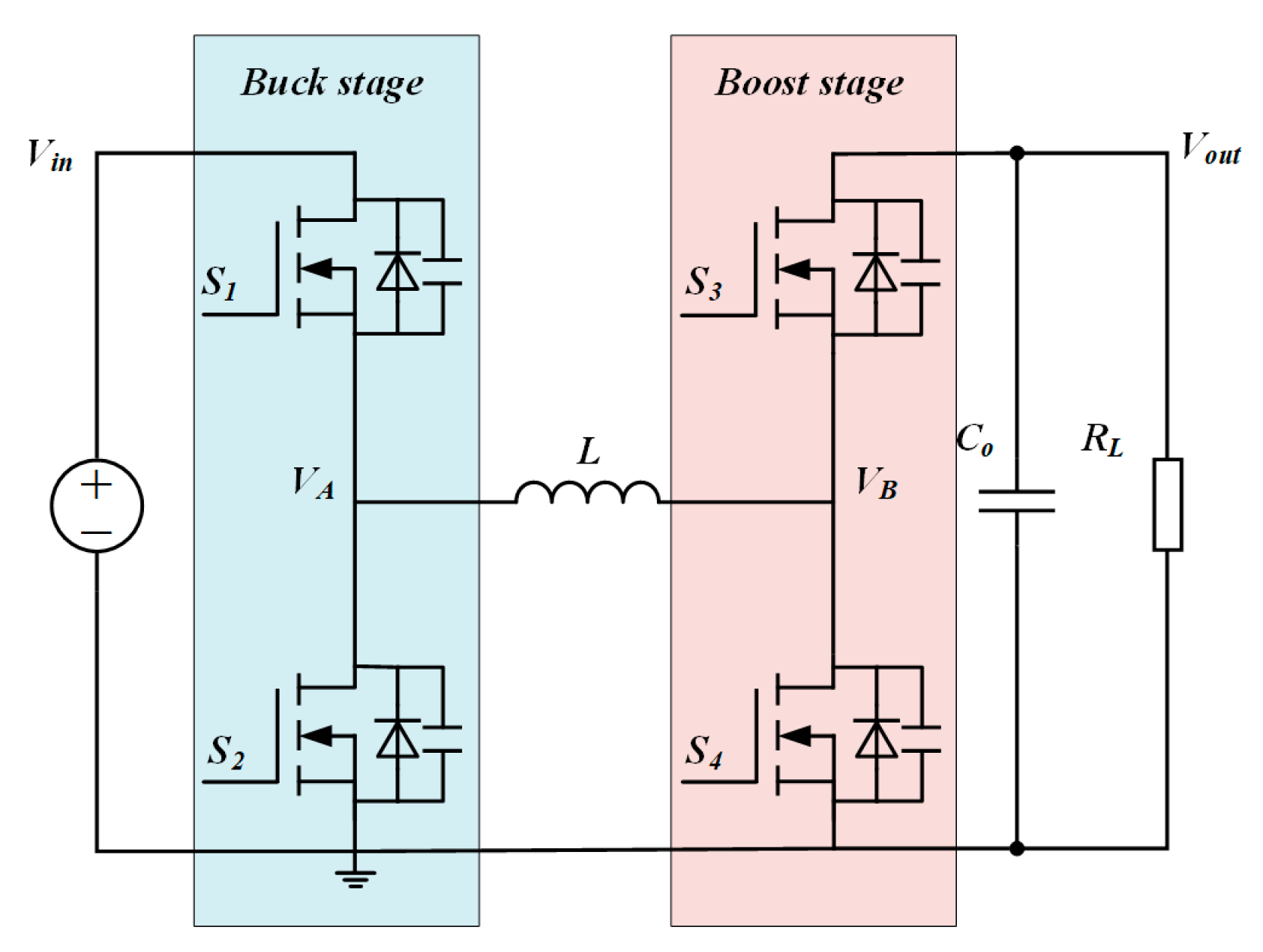
2.1. Principle of Multi-Mode Control

Dual-mode control is the simplest multi-mode control strategy, where the FSBB converter operates in either Buck mode or Boost mode by controlling the conduction of either S1 or S4 based on the input voltage. Since only one switch is in hard-switching mode in each of these operating modes, the switching losses are significantly reduced compared to single-mode control. Moreover, the inductor current ripple is also diminished, allowing the entire FSBB converter to achieve better efficiency [19,20].

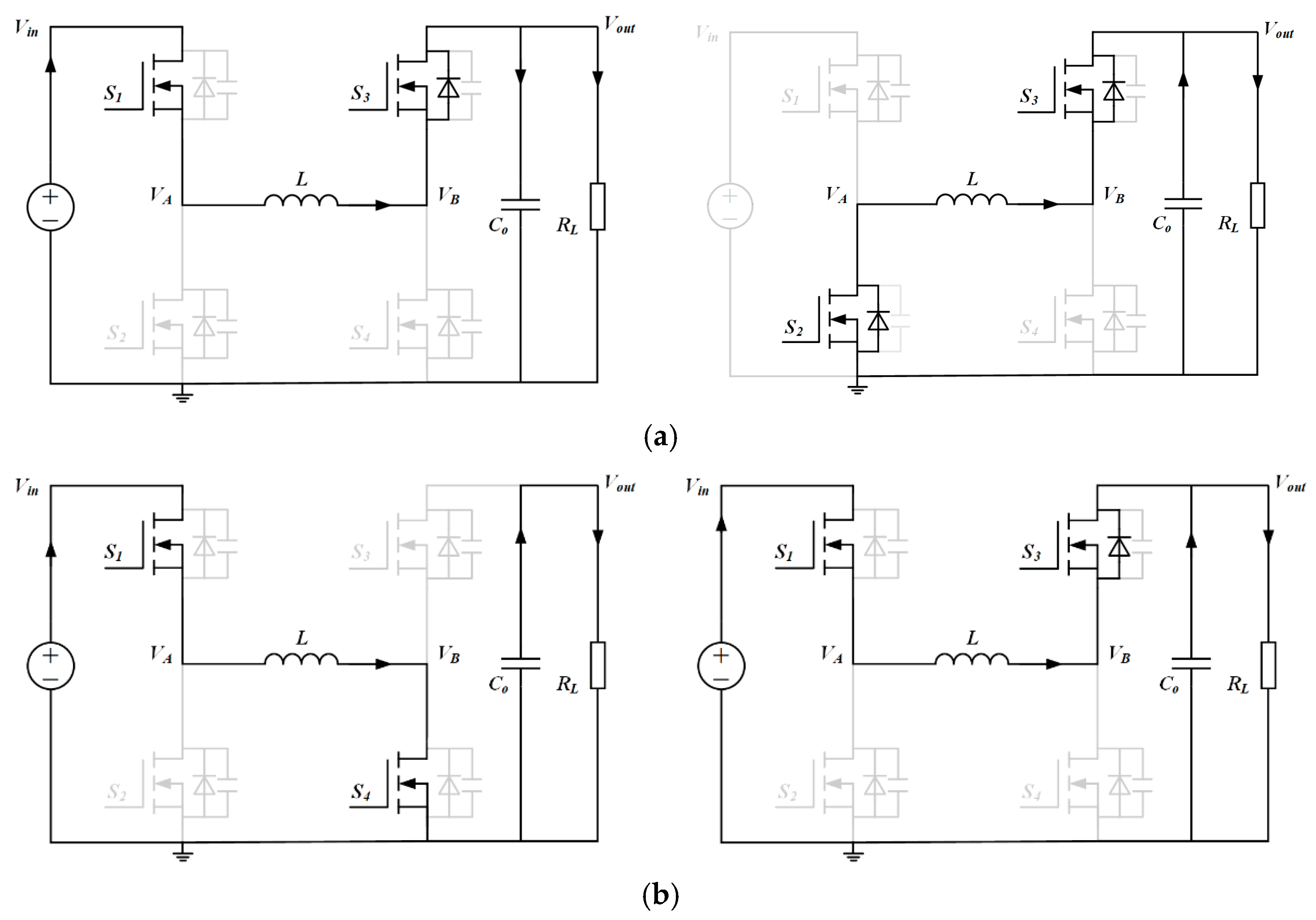
2.1.1. Dual-Mode Control Strategy

To address the issues associated with single-mode control, the dual-mode control strategy determines whether the FSBB converter operates in Buck mode or Boost mode based on the input voltage. When the input voltage is greater than the output voltage, the converter operates in Buck mode, with S3 always turned on and S4 always turned off while controlling the switching of S1. Conversely, when the input voltage is not higher than the output voltage, the converter operates in Boost mode, with S1 always turned on and S2 always turned off, controlling the switching of S3. The dual-mode controls are illustrated in Figure 3.
Figure 3 shows that in dual-mode control, only one switch is in operation during each mode. This significantly reduces the switching losses compared with single-mode control. Figure 4 compares the inductor current waveforms, voltage, and current waveforms of S3 in both single-mode and dual-mode simulations. The red line in Figure 4a,b represents the output voltage waveform, while the blue line represents the inductor current waveform; The red line in Figure 4c,d represents the waveform of the switch voltage, and the blue line represents the waveform of the switch current. The input voltage is 48 V, the output voltage is 75 V, and the switching frequency is 100 KHz. Compared to single-mode, dual-mode with only one bridge arm in the high-frequency switching state can significantly reduce inductor current ripple and the current stress on the switch. However, when the input and output voltages are close to each other, the converter may frequently switch between the two modes, which could lead to system instability. Additionally, the maximum duty cycle of the converter may be limited due to the influence of the parasitic parameters of the components and the delays in the controller.

2.1.2. Dead Zone Generated During Mode Switching

The presence of dead time not only leads to discontinuities in the voltage gain function but also causes output voltage ripple and oscillations near the mode transition points when the input voltage approaches these thresholds, resulting in system stability issues. These problems become particularly pronounced under high-power operation or sudden load changes, severely limiting the converter’s performance and reliability. Thus, understanding the cause of dead time and developing optimization methods is key to improving FSBB performance under multi-mode control.
Taking dual-mode control as an example, a unified control variable u (0 < u < 2) is introduced for analysis [21,22,23]. This control variable enables the integration of the ideal voltage gain M, the duty cycles of switches S1 and S4 (d1 and d2), and the input–output voltage ratio k. Table 1 describes the relationships among these three parameters under ideal conditions.
Figure 5a,b shows the variation of the duty cycle of the two bridge arms with u, with the black line being d1 and the red line being d2; Figure 5c,d shows the variation of voltage gain M with u. Under ideal conditions, the value of u is continuous over the entire range, allowing the two switches in each bridge arm to turn on and off simultaneously during mode transitions, resulting in a continuous voltage gain, as shown in Figure 5a,c. However, in practical circuits using dual-mode control, the presence of dead time between the duty cycles of the two switches in the same bridge arm, along with the effects of delays in the gate drive circuit and the switching devices’ turn-on and turn-off characteristics, leads to deviations [24,25]. The actual duty cycles and voltage gain characteristics are illustrated in Figure 5b,d.
When the duty cycle of the Buck mode d1 exceeds its maximum value d1max, d1 abruptly jumps to 1, creating a duty cycle gap between d1max and 1. Similarly, when the duty cycle of the Boost mode d2 falls below its minimum value d2min, d2 directly decreases to 0, resulting in a duty cycle gap between d2min and 0. Here, d1max represents the maximum duty cycle of the Buck bridge arm, whereas d2min denotes the minimum duty cycle of the Boost bridge arm. The constrained duty cycle region is commonly referred to as the “dead zone”, where the converter typically operates in a “direct-through state”, meaning that S1 remains permanently on while S4 stays permanently off. Consequently, the voltage gain M also becomes discretized.
Therefore, research on improving the multi-mode control strategy for the FSBB converter has focused primarily on the following: introducing various transition modes to eliminate the effects of the dead zone; reducing abrupt changes in the duty cycles of the switches in both bridge arms; ensuring a sufficiently smooth voltage gain and that the system can operate at a relatively high efficiency and have good dynamic response. However, the smoother the mode switching, the more complex the control strategy needs to be, which may have an impact on the efficiency and dynamic performance of the system. Therefore, trade-offs are usually needed in the process of improving the control strategy.

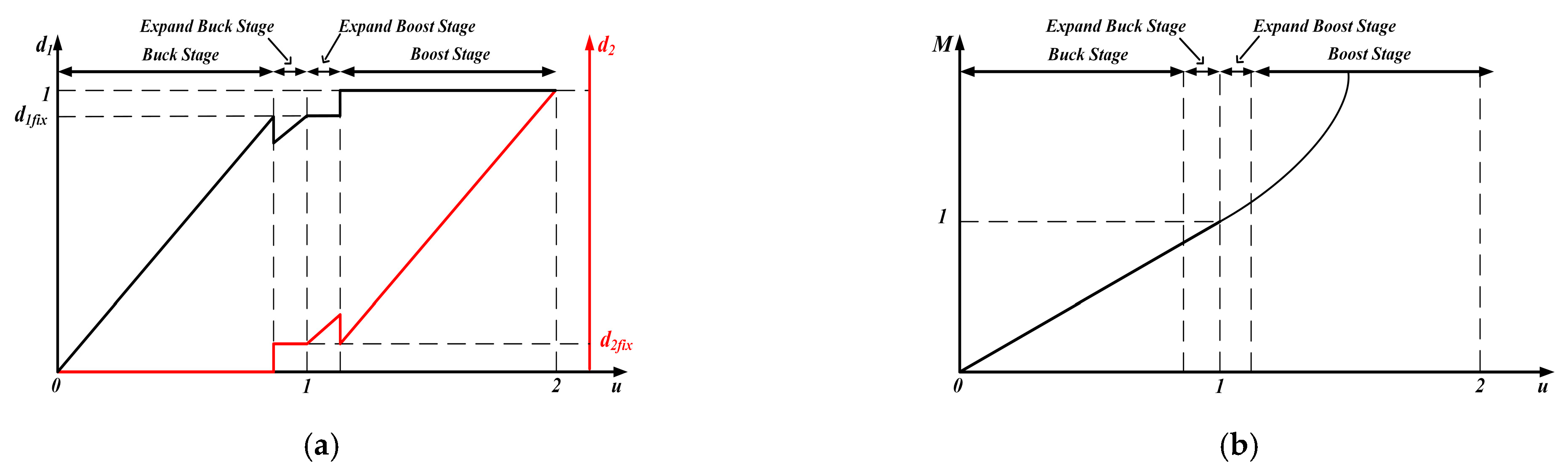
2.1.3. Three-Mode and Four-Mode Control

Subsequent research has focused on achieving smooth transitions between modes in the dual-mode control strategy. Many scholars have introduced a third or even fourth mode between Buck mode and Boost mode to facilitate the smooth transition of the FSBB converter between the two modes, thereby overcoming the effects caused by dead time.
References [26,27,28,29] employ a three-mode control strategy for the FSBB converter. When the input and output voltages are close, the converter operates in Buck–Boost mode, which simultaneously controls the conduction and cut-off of both bridge legs. At this point, the circuit’s working process is similar to that of single-mode control. Figure 6a shows the change of duty cycle of two bridge arms under the three-mode control, the black line is d1, and the red line is d2; Figure 6b shows the change of voltage gain M with u. This control strategy effectively eliminates sudden duty cycle changes caused by mode switching, improves the phenomenon of voltage gain mutation, and suppresses output voltage ripples. However, operating in the intermediate Buck–Boost mode still presents challenges related to large average values and ripples in inductor current. This may result in greater losses compared to the dual-mode control, although it improves system gain stability.
References [30,31] utilize a four-mode control method, which further subdivides the transitional mode in the three-mode strategy. When the ratio of input voltage to output voltage is defined as k = Vin/Vout, Δ 1 and Δ 2 are defined as a range of voltage fluctuations that can be confirmed through certain methods. If “ 1 Δ 1 < k < 1” is satisfied, the system operates under the extended Boost mode, fixing d1 = d1fix and adjusting d2. If “1 < k < 1 Δ 2 ” is satisfied, it operates under the extended Buck mode, fixing d2 = d2fix and adjusting d1. d1fix and d2fix represent the limits that the two duty cycles can reach under the dead time limit. Figure 7 shows the working principle and voltage gain of the four-mode control. The black line represents the duty cycle of d1, and the red line represents the duty cycle of d2. Through a more detailed division of the system operating range, this control mode can achieve smoother voltage gain changes than the three-mode control when the control parameters are selected reasonably. At the same time, in each expansion mode, only one bridge arm’s duty cycle is changing, which can slow down the changes in inductor current and reduce conduction losses. However, the control logic of four-mode control is complex; the control parameters that need to be determined increase and require multiple PWM signals to coordinate, placing high demands on sensor accuracy. Table 2 summarizes the core features and performance differences of these strategies:

2.2. Improve Control Algorithms and Control Logic

As mentioned earlier, three-mode and four-mode control strategies introduce transition modes to mitigate the effects of the dead zone. However, their practical implementation is not straightforward, as challenges arise in determining appropriate switching points for the transition modes and designing the operating states of both bridge arms within these modes. Researchers have sought to refine the control algorithms and logic of three-mode and four-mode strategies to optimize the selection of switching points and the design of transition modes. The objective of these methods is to ensure smooth mode transitions while maintaining high conversion efficiency and dynamic performance. The following section presents several recent methods proposed in the literature.

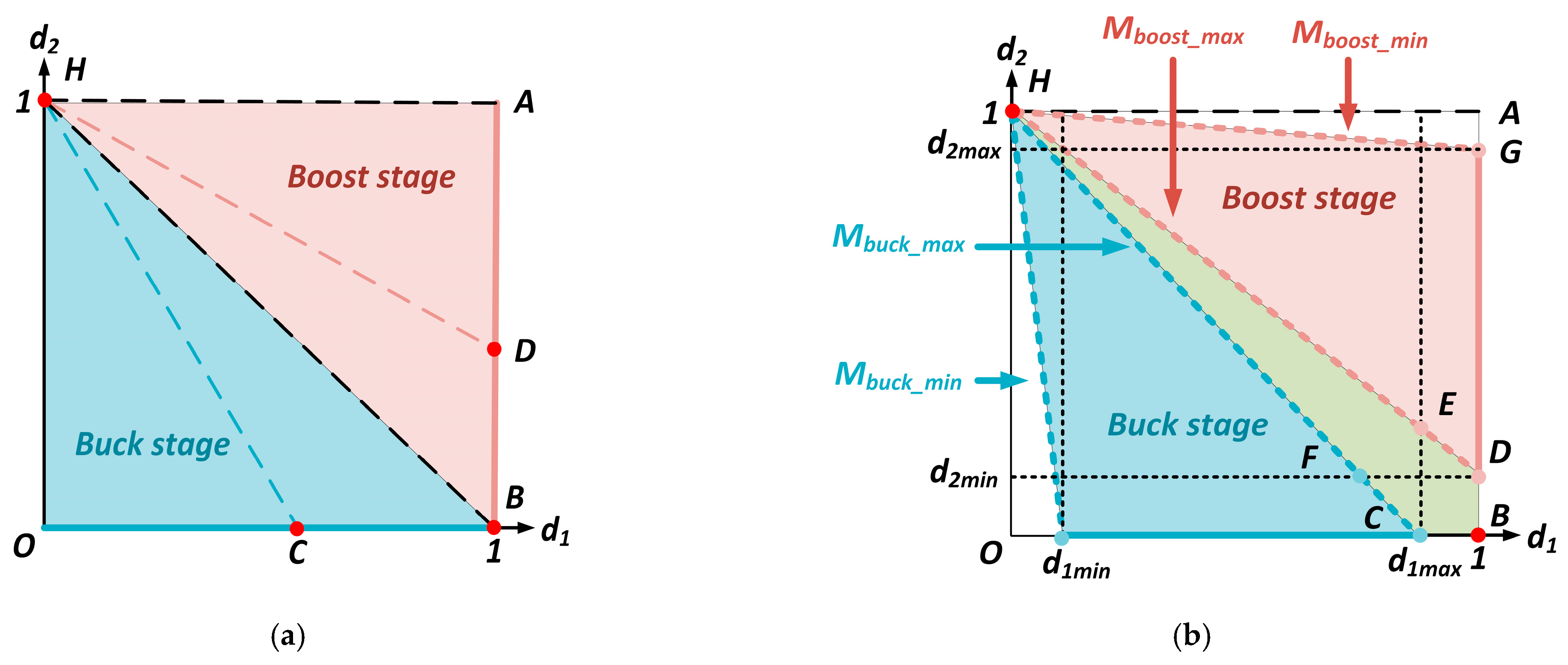
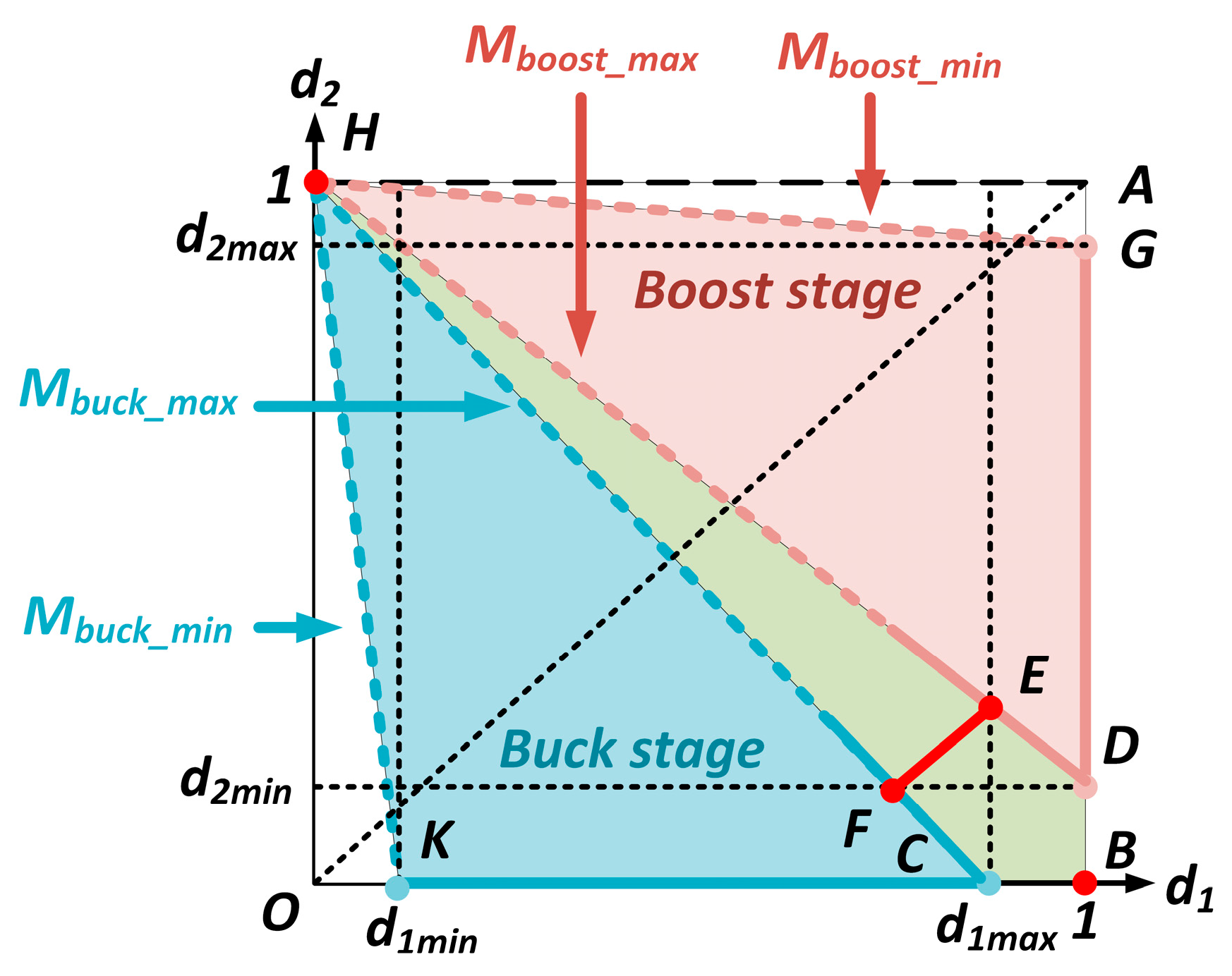
2.2.1. Three-Mode Smooth-Switching Strategy Based on a Graphical Method

As mentioned earlier, to eliminate the operational dead zone caused by mode switching in dual-mode control, a three-mode control strategy is introduced. Specifically, when the input and output voltages are relatively close, a third mode is incorporated, with the simplest implementation being the simultaneous switching of paired transistors, allowing the circuit to operate in the conventional Buck–Boost mode. However, studies [32,33,34] have noted that although this control strategy is easy to implement, it results in significant operational point jumps during mode transitions, leading to reduced system stability. To improve the performance of FSBB under three-mode operation, further investigation into the design of the transition mode is necessary. In references [32], a graphical method was proposed to describe the relationship between the duty cycles of the two bridge arms and the voltage gain of the FSBB converter. On the basis of this graphical approach, a smooth three-mode control strategy was developed. Figure 8 illustrates the relationship between the number of duty cycles and the voltage gain under both ideal and non-ideal conditions using this method.
By transforming Equation (3) into Equation (6), it can be observed that d1 and d2 exhibit a linear relationship, with a slope of k = 1 M .
d 2 = 1 M d 1 + 1
Therefore, if d2 is taken as the vertical axis and d1 is taken as the horizontal axis to plot the operating region of the converter, it can be observed that all duty cycle values fall within the quadrilateral enclosed by HOBA. According to Equation (6), the function graph of d1 and d2 must pass through point H (0, 1). Starting from point H, the set of line segments with different slopes terminating at any point on the OB or BA represents the possible duty cycle values for each fixed voltage gain, where the HB corresponds to the segment with a voltage gain of 1. Under ideal dual-mode control, this set of line segments can continuously move from the HO along the OBA to the HA without any blind spots, as illustrated in Figure 8a. However, when considering the practical constraints of the maximum and minimum duty cycle values for both bridge arms, continuous movement of this segment is not possible, as indicated in Figure 8b. The green and blank areas in the figure represent regions that cannot be uniformly varied due to limited duty cycle.
Several studies have utilized this graphical method to describe the operating region of converters [13,35,36], providing a basis for discussing the smooth transition strategy of the three-mode control. The previously mentioned method of simultaneous switching of paired transistors in three-mode control is illustrated in Figure 9a, where the converter’s operating trajectory is represented by a KCF1E1DG. Significant jumps in the duty cycle occur when transitioning from C to F1 or from when E1 transitions to D, which can lead to discontinuities in voltage gain. References [12,37] indicate that fixing the duty cycle of either the Boost stage or the Buck stage in the intermediate mode can be beneficial. Figure 9b presents the operating trajectories for the two methods, demonstrating a substantial improvement in the reduction in duty cycle jumps.
Based on Figure 9, it can be concluded that the closer the operating point during mode switching is to the critical operating points F and E of the Buck and Boost modes, the smaller the changes in the duty cycles of the two bridge arms will be, resulting in smoother mode transitions and more continuous voltage gain. Therefore, when a control mode is added only in the blind area, one can choose to directly connect the two boundary points E and F of the voltage gain blind area with a straight line, representing the trajectories of duty cycles d1 and d2, to minimize the variation in duty cycles during mode switching. Consequently, Reference [32] introduces an improved smooth transition control strategy, as illustrated in Figure 10, with its operating trajectory represented by KCFED.
If d1max and d2min are known, the relationship between d1 and d2 in the blind spot can be obtained:
d 2 = A d 1 + B A = 1 d 1 m a x + d 2 m i n 1 d 1 max d 2 min B = d 1 max d 2 min + d 1 m a x 1 1 d 2 min 2
Reference [32] points out that the inductance current ripple under all control strategies is unionized based on the inductance current ripple under the single-mode control as the reference value. Under the condition of Vout = 48 V, 30 V ≤ Vin ≤ 70 V, Pout = 3300 W, fs = 100 kHz, L = 12 µH, d1max = 0.95, d2min = 0.05, this three-mode smooth-switching strategy within the full input voltage range is the control method with the smallest inductance current ripple among all three-mode control strategies. At the same time, it is superior to some four-mode controls and achieves a good balance between the control mode and the inductance current’s ripple size.

2.2.2. Frequency-Varying Loop Selection Control Strategy Based on Four-Mode Control

Chapter 2 briefly introduces the principles of the four-mode control strategy. In this section, further analysis is conducted to discuss how this strategy mitigates the impact of the operational dead zone, determines mode transition points, and selects the duty cycles of both bridge arms in the extended modes.
Reference [36] proposed a frequency-varying loop selection control strategy based on four-mode control, providing both mode transition points and duty cycle selection for the extended modes of both bridge arms. This strategy first introduces the Buck-T and Boost-T modes on the basis of conventional two-mode control, which are similar to the previously mentioned extended Buck and extended Boost modes, thereby forming a four-mode control approach that effectively eliminates the dead zone effect. Second, optimizing the switching boundaries and applying minor frequency variation control helps address efficiency degradation caused by the intermediate mode. Finally, a switch-selection control strategy incorporating an input voltage feedforward is designed to further improve the performance of multi-mode control.
To ensure the continuity of the converter’s output voltage gain, d 2 fix should be fixed at d 2 min in Buck-T mode, whereas d 1 fix should be fixed at d 1 max in the Boost-T mode. By analyzing the inductor current ripple in the intermediate mode under different switching boundaries and the proportion of direct power transfer phases, the operating regions of the FSBB converter for different modes over a wide input voltage range are ultimately derived, as expressed in Equation (8).
V i n = 0 < V i n < V o u t 1 d 2 min B o o s t V o u t 1 d 2 min < V i n < V o u t 1 d 2 min d 1 max   B o o s t T V o u t 1 d 2 min d 1 max < V i n < V o u t d 1 max       B u c k T V o u t d 1 max < V i n B u c k
This strategy employs a small-range variable frequency control in the intermediate mode to increase efficiency. The overall system loss is determined by the root mean square (RMS) value of the inductor current and the switching frequency of the power switches. By analyzing the variation in the inductor current RMS value with the input voltage and switching frequency, the optimal switching frequency for the two transition modes is derived, where f base represents the system’s base frequency. A unified small-signal AC model for the FSBB converter under multi-mode operation is subsequently derived via the state–space averaging method. This model establishes the relationship between the system transfer function and mode transitions, leading to the design of two compensation networks, G c 1 S and G c 2 S , which improves system stability. Additionally, an input voltage feedforward compensation G ff S is introduced to mitigate the impact of duty cycle variations on the output voltage. The control block diagram is shown in Figure 11, where G M S represents the PWM transfer function, H ( S ) denotes the transfer function of the output voltage sampling network, and G vd S and G vg S represent the transfer functions of the duty cycle and input voltage to the output voltage, respectively. Figure 11 shows the overall control diagram.
Reference [36] compares the peak efficiency of three configurations—the traditional three-mode, traditional four-mode, and frequency-varying loop selection four-mode—in the transition mode in the experiment, which are 92.3%, 94.8%, and 96.3%, respectively. It points out that compared with the traditional multi-mode control strategy, the operation efficiency of the system in the intermediate mode can be improved by selecting the controller according to the corner conditions of the system model and adjusting the operating frequency in the transition mode.
Reference [38] employs a similar variable frequency control method based on the three-mode operation, incorporating an input voltage feedforward. By detecting input voltage variations, different feedforward loops are automatically selected to suppress the impact of input voltage disturbances on the output voltage. Additionally, the reference voltage setting is optimized to eliminate output voltage transients during mode transitions. However, this strategy may impose a high real-time computational burden on the system and relies heavily on precise sensors. Inaccurate sensor readings could lead to poor dynamic performance and incorrect mode transitions. Moreover, this method considers only the losses in the transition mode without accounting for the overall converter losses. Similarly, Reference [35] analyses the relationship between the inductor current ripple and bridge arm phase shift time under four-mode control with a maximum duty cycle, deriving the operating conditions for minimizing the inductor current ripple. Furthermore, a loss model for the FSBB converter is established, and a low-ripple frequency-reduction control strategy is proposed. This strategy reduces the switching frequency during transition modes, thereby improving the overall efficiency of the FSBB converter.

2.2.3. Model Predictive Control Base on Four-Mode Control

In recent years, Model Predictive Control (MPC) has been increasingly applied in the field of power electronic converter control due to its advantages of fast dynamic response and simple design [39,40,41]. When MPC is applied to the control of FSBB converters, it offers two main benefits. First, the predictive mechanism of MPC enhances the dynamic performance. Second, by predicting the system states of the FSBB converter under different operating modes, MPC facilitates the selection of the most suitable operating mode, thereby simplifying mode transition control.
In [42], MPC was utilized in a four-mode control strategy to achieve inductor current predictive control across all four operating modes. Based on the predicted duty cycle results for different modes, the most suitable operating mode is selected to enable seamless mode transitions. As shown in Figure 12, Vo,ref and iL,ref represent the reference values for the voltage outer loop and current inner loop, respectively.
The inductor current predictive control based on MPC offers the following advantages: (1) Fast dynamic response; (2) Capability of achieving fixed-frequency control; (3) The predictive mechanism of MPC enables the selection of the most suitable operating mode without the need for additional mode-switching detection. However, the core of MPC lies in real-time computation and optimization. Particularly in multi-mode prediction, it is necessary to compute the predicted values for multiple operating modes within each control cycle and select the optimal mode. This computational complexity may impose high real-time requirements, especially in scenarios with limited hardware resources. Additionally, the performance of MPC is highly dependent on the accuracy of the system model. If actual system parameters (such as Inductance, capacitance, and load resistance) deviate from the assumed model, prediction inaccuracies may arise, thereby affecting the overall control performance.
In order to improve the multi-mode control strategy, the existing research mainly focuses on the three-mode or four-mode control, whose main goal is to reduce the overall converter loss, improve the dynamic performance, and ensure continuous voltage gain. The study discussed how to select mode-switching points, determine appropriate mode-switching methods, and design transition modes (Table 3). In practical engineering applications, a comprehensive consideration of different requirements and constraints is necessary to determine the most suitable approach.

2.3. The Problems of Multi-Mode Control Under Hard Switching

Although multi-mode control under hard switching enhances the adaptability and efficiency of the four-switch Buck–Boost (FSBB) converter by dynamically switching between Buck, Boost, and transition modes, several challenges remain in practical applications:
(1) Uneven voltage stress in transition mode. In multi-mode control, the introduction of transition modes may lead to uneven voltage stress across different switching devices. For example, during rapid input voltage fluctuations, switches in the Buck leg may experience prolonged high-voltage stress, whereas switches in the Boost leg may undergo frequent transitions, resulting in concentrated thermal stress. This imbalance not only accelerates device aging but also increases the risk of localized failure, reducing system reliability. Additionally, the bidirectional inductor current in transition mode may exacerbate parasitic resonance effects, further amplifying voltage spikes. A dynamic duty cycle allocation strategy can be employed to mitigate the voltage stress imbalance. In transition mode, the overlap interval of the Buck and Boost legs’ duty cycles can be adjusted on the basis of real-time input voltage and load conditions to ensure an even distribution of voltage stress among switches. Furthermore, active voltage balancing circuits can be introduced to absorb spike energy at high-voltage nodes, thereby protecting the switches. Moreover, redundant designs, such as parallel low-voltage switches, can help share current in high-voltage paths, effectively reducing the stress on individual devices and extending their lifespan.
(2) Limited real-time coordination in multi-mode operation. As the number of operating modes increases, the control algorithm must complete mode identification, switching decisions, and parameter adjustments within microsecond-level time constraints. Traditional centralized control architectures may experience response delays due to limited computational resources, especially during sudden input voltage changes or load transients, which can lead to mode-switching lag and cause output voltage overshoot or oscillation. For example, in renewable energy applications, rapid fluctuations in photovoltaic input power may prevent the controller from switching to the optimal mode in time, thereby reducing efficiency. To address this issue, a distributed intelligent control architecture can significantly enhance real-time performance. By decomposing control tasks into multiple submodules (e.g., mode identification, duty cycle generation, and fault protection), each managed by dedicated hardware, parallel processing can be leveraged to shorten the decision-making time.
(3) Persistent hard-switching operation. Regardless of whether the system operates in a single-mode or multi-mode configuration, all four switches remain under hard-switching conditions in the aforementioned control strategies. Although various optimization techniques can reduce conduction losses in transition mode, they do not eliminate hard switching entirely. With the rapid advancement of wide-bandgap (WBG) power semiconductors, which enable higher switching frequencies, continuing to operate under hard-switching conditions will lead to significant conduction losses. Consequently, recent research has focused on achieving zero-voltage switching (ZVS) for system switches, serving as a foundation for further performance optimizations.

3. Research on a Control Strategy Under Soft Switching

A control strategy based on soft switching has been proposed to achieve zero-voltage switching (ZVS) for all four switches by shaping the inductor current waveform. Compared with the multi-mode control under hard switching discussed earlier, this approach further improves the converter’s efficiency and enables higher-frequency [43,44,45]. This chapter begins with the fundamental principles of ZVS implementation, introducing how the FSBB achieves soft switching, followed by an analysis of the new challenges arising from this approach and the corresponding improvements proposed by researchers.

3.1. Process of Implementing Soft Switching in the FSBB

In an ideal scenario, it is typically assumed that the switching transitions occur instantaneously—when a switch turns on, the voltage across it drops to zero instantly while the current rises immediately; conversely when it turns off, the voltage rises instantly while the current drops to zero. However, in practical applications, owing to turn-on and turn-off delays as well as the presence of the switch’s input and output capacitances, achieving this ideal state is impossible. As a result, conduction and switching losses always occur, which become more significant as the switching frequency increases.

3.1.1. Implementation Principle of ZVS

The essence of zero-voltage switching (ZVS) is to utilize the inductor current during each switching cycle’s dead time to discharge the output capacitance of the switch that is about to turn on. This ensures that the voltage across the switch is close to zero when the dead time ends, enabling soft switching. On the basis of the timing analysis in Figure 13, each dead time interval enables the zero-voltage turn-on of a specific switch. In Figure 13, T d 1 ~ T d 4 represents the dead time interval, and i 1 ~ i 4 denote the inductor current at the beginning of each dead time. To achieve ZVS for all four switches in the FSBB converter, the following conditions must be satisfied:
i 1 , i 2 ,   i 3 ,   i 4 I Z V S
I Z V S = max V i n , V o u t 2 C O S S L
I ZVS represents the minimum inductor current required to fully charge or discharge the output capacitance C OSS of the two switches in a half-bridge configuration to achieve ZVS [46].

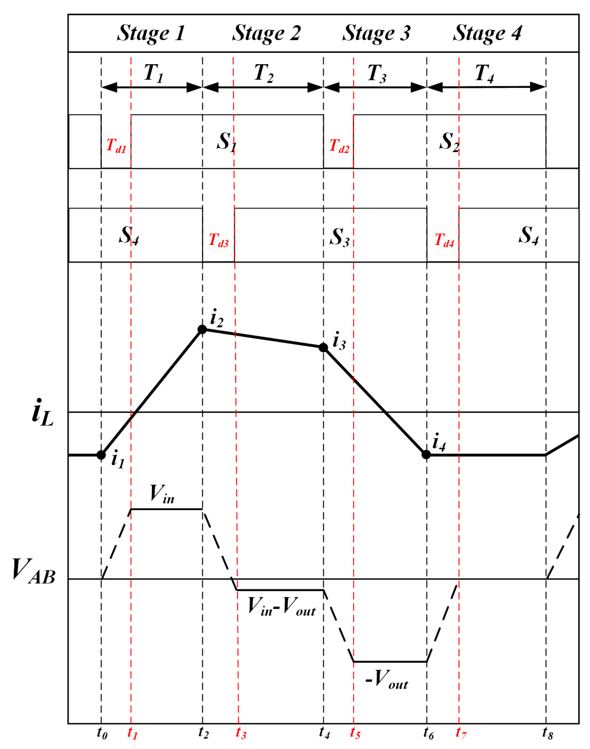
3.1.2. Working Principle of Quadrilateral Inductor Current Control Strategy

The quadrilateral inductor current strategy, proposed in [47], is widely used to achieve ZVS for all four switches in FSBB converters. This section introduces the principle of this control strategy and explains how soft switching is achieved by shaping the inductor current waveform.
By adjusting the phase shift δ between the duty cycles of the Buck and Boost stages, the inductor current forms a quadrilateral waveform with a negative current phase, ensuring operation in the forced continuous conduction mode (FCCM). This sequentially enables ZVS for the switches [48,49,50]. As shown in Figure 2, let V A denote the midpoint voltage of the Buck stage formed by switches S1 and S2, and let V B denote the midpoint voltage of the Boost stage formed by switches S3 and S4. The inductor L is connected between these two midpoints. Depending on the switching sequence of S1, S2, S3, and S4, the voltage across the inductor, V AB , can take one of four possible values: V in , V in V out , V out , or zero voltage. These correspond to the four operating phases illustrated in Figure 11, with their respective time durations defined as T 1 , T 2 , T 3 and T 4 . The current slope in each phase is given by the following:
i L = V i n L · T 1                                   s t a g e   1 V i n V o u t L · T 2         s t a g e   2 V o u t L · T 3                       s t a g e   3 0                                                       s t a g e   4
In each stage, the inductor current varies linearly according to the voltage applied across the inductor. The conduction states of the switches in each stage are shown in Figure 12.
Figure 14 shows the working state of the circuit and the implementation process of the soft switch during each period of time in Figure 13. In the interval from t0 to t1, the inductor current is negative, discharging the junction capacitance of switch S1 while charging the junction capacitance of switch S2. During this time, the voltage across S1 approaches zero, enabling ZVS for S1 at time t1. The interval from t1 to t2 is the energy charging phase, during which the voltage across the inductor is V i n , causing the inductor current i L to increase linearly. From t2 to t3, the inductor current discharges the junction capacitance of switch S3 while charging the junction capacitance of switch S4. At time t3, the voltage across S3 is nearly zero, allowing ZVS for S3. The interval from t3 to t4 is the direct power transfer phase, during which the voltage across the inductor is V in V out , and the change in i L depends on the relationship between the input and output voltages, increasing or decreasing linearly. The subsequent intervals t4 to t5 and t6 to t7 similarly utilize the inductor current to charge and discharge the junction capacitances of the corresponding switches, ensuring ZVS for the next switch that will be turned on, which will not be elaborated further here. The interval from t5 to t6 is the reset phase, during which the voltage across the inductor is V out , causing i L to decrease gradually from a positive value to a negative value. The interval from t7 to t8 is the freewheeling phase, during which the voltage across the inductor is zero, and i L remains constant at a negative value. By precisely controlling the duration of these phases, the ripple of the inductor current can be reduced, enabling ZVS for all switches and thereby enhancing the efficiency and performance of the converter.

3.2. The Main Optimization Directions of Current Research

Before discussing the optimization of control strategies under soft switching, it is essential to provide a brief overview of their core optimization objectives. The optimization of soft-switching control strategies will address the following issues:
(1)
Potential loss of ZVS under varying operating conditions:
The primary goal of implementing zero-voltage switching (ZVS) is to reduce hard-switching losses in the switches, allowing for higher switching frequencies and greater power density. However, changes in load or the direction of power transfer can lead to the loss of ZVS in certain situations [51,52].
(2)
Further Reduction of System Losses:
Although the conduction losses of the switches are nearly eliminated under this control strategy, other losses still occur within the system, primarily due to the conduction losses associated with inductor current and thermal losses caused by current-sensing resistors. These factors can limit the system’s efficiency and power density. Typically, loss models are established by calculating the average inductor current in the time or frequency domain [53] to determine the relevant control parameters.
(3)
Challenges in Achieving Good Dynamic Performance and High Computational Demand:
ZVS requires precise calculations of the switching times for each stage and real-time adjustments to the phase differences. During load transients or power direction reversals, the inductor current may experience overshoot or interruption. Additionally, high-precision current sensing is crucial for effectively implementing this control strategy. These challenges significantly increase the computational load, placing greater demands on the system’s processing speed.
From Section 1 and Figure 13 and Figure 14, it can be seen that the selection of the four time periods, T1 to T4, determines the implementation of the system’s soft switch and the RMS value of the inductor current. These four stages are determined by the duty cycles of both bridges and the timing difference of their driving signals. Therefore, it is necessary to model the system first and determine these three parameters reasonably according to different working conditions. The dynamic response speed of the system is determined by multiple factors, including but not limited to the complexity of parameter calculation methods, the design of control loops, software architecture, and the clock frequency of the MCU. Based on these, researchers have proposed various solutions from multiple perspectives.

3.3. Optimizing the Implementation of ZVS

In converters, the implementation of zero-voltage switching (ZVS) relies on proper control of the inductor current. This section summarizes two ZVS failure scenarios and corresponding improvements.

3.3.1. Loss of ZVS Due to Small Inductor Current Ripple

As previously mentioned, to achieve ZVS, the junction capacitance of the switches must be charged and discharged within the dead time, which requires the inductor current to reach I Z V S before the dead time. If the inductor current ripple remains constant across the entire load range, ZVS may be lost during light load conditions or when Vin and Vout are nearly equal. The FSBB converter has three control variables: the duty cycle of the Buck leg, the duty cycle of the Boost leg, and the phase-shift duty cycle between the two legs. By utilizing these three control variables, Reference [47] proposed a constant-frequency quadrilateral inductor current control strategy that combines pulse-width modulation and phase-shift modulation. This approach adjusts the duty cycles and phase differences of the driving signals for the two stages to ensure that the inductor current is sufficiently large to discharge the charge in the switch capacitance before the dead time arrives. Using this control scheme, all power switches can achieve ZVS across the entire input/output voltage and load range. This strategy has also been adopted in several subsequent studies [44,45,54,55,56], although it does not address the smooth transition of the power transfer direction.

3.3.2. Loss of ZVS Due to Reversal of the Power Transfer Direction

The FSBB converter can achieve bidirectional power transfer; however, switching the direction of power transfer may lead to an overshoot of the inductor current, resulting in the loss of ZVS. Reference [57] derives the voltage conditions and ZVS criteria on the basis of the volt-second balance and details the key waveforms in the pseudo-critical continuous current mode (PCRM) and pseudo-discontinuous current mode (PDCM) during the forward power transfer operation. Unlike DCM and BCM, which are mentioned below, the inductor current may be negative at some points or time periods. To enable a smooth reversal of the power transfer direction in the FSBB converter, it is essential to choose an appropriate triggering moment. Triggering the reversal while S2 and S4 are conducting can achieve an optimal switching sequence, avoiding current overshoot and ensuring ZVS. At the moment of the reversal trigger, the reference values for the regulators generating the driving signals for S1 and S2 (forward transfer) or S3 and S4 (reverse transfer) are set to zero and then gradually increase to the desired value. This reduces the output of the regulator, thereby decreasing the duty cycle of S1 (forward transfer) or S3 (reverse transfer), preventing inductor current overshoot and ensuring ZVS for the power switches.

3.4. Reducing System Losses

Reducing overall system losses is a key research focus in soft-switching control strategies. This subsection summarizes methods proposed in various studies to improve system efficiency from two perspectives.

3.4.1. Reducing Losses by Determining Optimal Control Variables Through Mathematical Modelling

Establishing a loss model for the FSBB converter to determine the optimal control variables (T1~T4) has become a commonly used approach in recent studies. Reference [43] investigated the principle of minimizing the peak current in an FSBB converter operating in boundary conduction mode (BCM). This means that the inductor current returns to zero at the end of each switching cycle. It analyses the variation in inductor current under different operating conditions and determines the optimal control variables through mathematical modeling, effectively minimizing the peak inductor current and reducing losses associated with the inductor current. In addition, distinguishing operating states based on inductor current waveform usually includes continuous conduction mode (CCM) and discontinuous conduction mode (DCM). They respectively mean that the inductor current is greater than zero throughout the entire working cycle and will remain zero for a certain period of time. Reference [58] explores the selection of optimal control variables in both DCM and CCM to ensure that the RMS value of the inductor current is minimized, thereby reducing the associated losses. The ranges of each reference variable are given in Equation (12).
T 1 V o u t + max V i n , V o u t · 2 · L · C o s s V i n T 3 V i n + max V i n , V o u t · 2 · L · C o s s V o u t T 1 + T 3 T s
The literature indicates that selecting control variable values that satisfy the aforementioned constraints enables ZVS. Next, to further refine the range of these variables, the objective is set to minimize the RMS value of the inductor current. The expression for the inductor current iL over one switching cycle is given by the following:
i L t = I Z V S + V i n L t                                                                                                                                             ( 0 < t t 2 ) I Z V S + V i n L T 1 + V i n V o u t L t T 1                                                                                       ( t 2 < t t 4 ) I Z V S + V i n L T 1 + V i n V o u t L T 2 V o u t L t T 1 T 2           ( t 4 < t t 6 ) I Z V S                                                                                                                                                                         ( t 6 < t t 8 )
On the basis of the volt–second balance of the inductor, the relationship between the voltage gain M and the control variables T1 to T3 can be derived. Similarly, applying the charge balance principle to the capacitor allows for the determination of the relationship between the output current Iout and T1 to T3. Ultimately, the optimal combination of control variables that minimize the RMS value of the inductor current can be obtained, thereby reducing the associated losses to the lowest possible level. However, this mathematical model considers only losses caused by the inductor current while neglecting other factors such as turn-off losses, driving losses, and losses introduced by the inductor components themselves. These factors also impose limitations on efficiency improvement.
To address this, Reference [59] proposes a high-efficiency multi-mode control strategy on the basis of the aforementioned analysis. A comprehensive loss model was developed, taking into account conduction losses, turn-off losses, driving losses, and inductor component losses. The control strategy was optimized with the objective of minimizing total losses. Furthermore, a data-fitting approach was employed to establish dynamic relationships between the control variables and parameters such as input voltage, output voltage, and load current. This enables a multi-mode control scheme that maintains a constant frequency under light loads, a variable frequency under medium loads, and frequency reduction under heavy loads, achieving unprecedented efficiency improvements. In Reference [59], a 300 W prototype was built and used to determine the control variables. The test results showed that the experimental prototype could achieve high conversion efficiency in the full input, output voltage range, and full load range. The maximum peak efficiency reaches 98.5%, the highest average efficiency reaches 97.93%, and the switching frequency can reach up to 500 kHz–1 MHz.

3.4.2. Reducing Losses Caused by Current Sensing Resistors

In FSBB control, real-time sampling of the inductor current is needed, which is typically achieved by inserting a sensing resistor in the main current path. However, this approach introduces additional power loss, reducing the overall efficiency of the converter. Reference [60] proposed a lossless current sensing method based on the volt-second principle. By detecting the switching node voltage and utilizing the capacitor charging current to indirectly represent the inductor current, this method eliminates the power loss associated with traditional sensing resistors. The proposed method employs two voltage-controlled current sources and a charging capacitor, Ct, where the voltage across the capacitor VCt is used to indirectly indicate the inductor current iL. This technique not only achieves lossless current sensing but also simplifies the control logic, enhancing the overall performance of the converter.

3.5. Improving the Computing Speed and Dynamic Performance
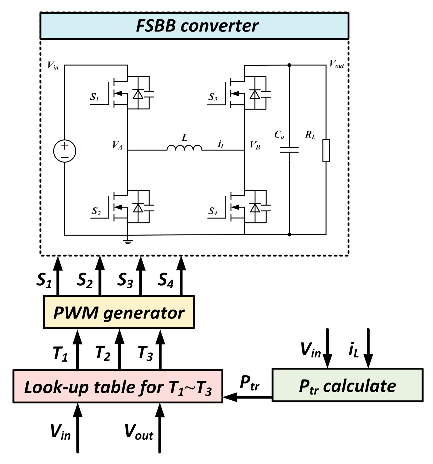
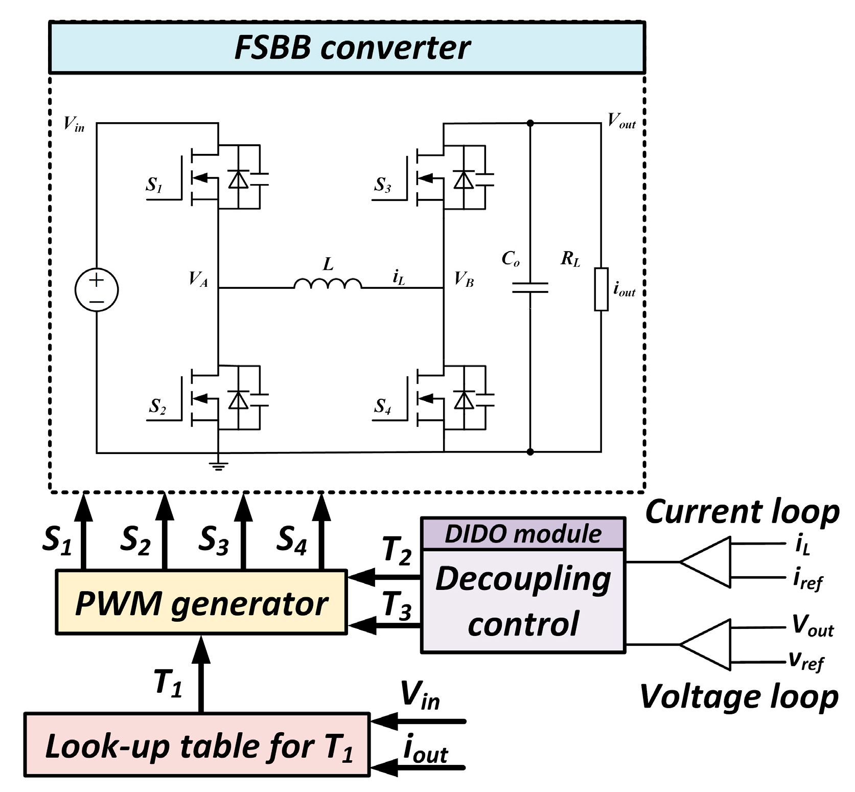
The adoption of soft-switching control strategies significantly increases the computational burden of the system. Increasing computational speed and improving the dynamic performance of devices have become key research focuses in recent years.

3.5.1. Lookup Table

The lookup table (LUT) method is a commonly used technique in the modulation strategies of power electronic converters, aiming to reduce the complexity of real-time computations. By precomputing and storing control variables corresponding to different operating points, the required control variables can be rapidly retrieved during real-time control, thereby achieving efficient power conversion. In [47], switching times T1, T2, and T3 were precomputed for various input voltages, output voltages, and power transfer levels and stored in a 3-D lookup table. In the controller software, the number of switches is obtained from the lookup table via linear interpolation on the basis of the current operating point. High-precision zero-crossing detection or high-speed analogue comparators are subsequently used to monitor the half-bridge voltage, ensuring that the inductor current RMS value is minimized and that the switching devices operate under zero-voltage switching. The control process is illustrated in Figure 15. However, due to strong variable coupling, relying on a single 3D LUT leads to complex processing.
References [55,56] improved the control architecture by decoupling the control variables, thereby reducing computational complexity. In this approach, the control variable T1 is precomputed for different operating points and stored in a 2-D lookup table. During real-time operation, the controller retrieves T1 from the 2-D lookup table, while the T2 and T3 values are dynamically calculated and adjusted in real time via a DIDO module to achieve ZVS and regulate the output voltage. The control block diagram is shown in Figure 16.
While the lookup table method reduces computational complexity, it requires a significant amount of memory space on the processor to obtain accurate calculation results. This can lead to increased costs and greater system complexity.

3.5.2. Simplified Real-Time Calculation Method

To reduce storage resource costs and further simplify system complexity, Reference [58] proposed a simplified real-time calculation method. By dividing the discontinuous conduction mode (DCM) and continuous conduction mode (CCM), this method achieves a minimal RMS inductor current and ZVS operation without complex calculations or mode transitions. This approach avoids the costs associated with external storage devices and meets transient demands.
The literature indicates that in the DCM, the inductor current does not transfer power during segment T4, resulting only in conduction losses. Therefore, maintaining the inductor current at a minimum negative value of I ZVS during T4 minimizes conduction losses. In contrast, during CCM, the current in T4 is zero, allowing for continuous power transfer throughout the cycle. By analyzing the inductor current waveform, a relationship between the RMS value of the inductor current and the peak current is derived in DCM, revealing that the conditions for the minimum RMS value correspond to the inductor current values of I ZVS during either the T1 segment (Boost mode) or the T3 segment (Buck mode). By fixing T1 or T3 as a constant, the calculation of control variables is simplified, and a PI controller is used to adjust the output voltage, with the output of the PI controller directly used as T2, thus enabling straightforward closed-loop control. However, this method employs variable frequency control, which complicates the design of the system’s EMI filter.
Reference [61] also introduced a new nonlinear average model that describes the dynamic behavior of the FSBB on the basis of the change in inductor energy and provides a more accurate depiction of the impact of phase shift on system dynamics. Within a switching cycle, the change in inductor energy equals the difference between input energy and output energy. A new state variable, i e , is introduced to represent the average of the initial and final values of the inductor current over one cycle. On the basis of the energy balance relationship, expressions that relate input and output currents to the overlapping duty cycle regions of the two bridge arms and the phase shift are derived. This method accurately captures the impact of phase shift changes on the inductor current and output voltage, introduces the new state variable i e , and avoids the complexities of traditional methods that require low-pass filters or complicated calculations to obtain the average current.

3.5.3. Approximate Duty Cycle Phase Shift Method

In traditional PWM with phase-shift control, the calculation of the phase-shift duty cycle δ is often quite complex. The phase-shift duty cycle determines the time difference between the switching of S1 and S3, which in turn affects the waveform of the inductor current. Reference [54] proposed an approximate duty cycle phase-shift method, deriving the theoretical expression for the phase-shift duty cycle δ and presenting an approximation technique. By employing a Taylor series expansion and retaining the first-order derivative term, this method simplifies the complex nonlinear relationship into a linear relationship.
δ a p p r = a · V i n + b · I o + b
In this method, coefficients a, b, and c are fitted on the basis of boundary conditions such as the maximum input voltage and maximum output current. This approximation allows for real-time computation of δ without the need for complex closed-loop control or lookup tables, significantly simplifying the implementation of the control circuit. This approach ensures that under all operating conditions, δ a p p r is always greater than the theoretical value, thus guaranteeing zero-voltage switching (ZVS) for all power switches. Moreover, since the approximate δ can be adjusted in real time, the FSBB converter can respond quickly to rapid changes in load or input voltage, maintaining ZVS and enhancing dynamic performance. Various computational methods under soft-switching control are summarized in Table 4:

3.6. Current Issues and Possible Solutions

While soft-switching control achieves efficient soft switching through phase shift adjustment, several potential issues remain in its optimization process, which may not have been adequately addressed in current research:

3.6.1. Destructive Impact of Inductor Parameter Tolerance on ZVS

In practical applications, manufacturing deviations in inductor values or temperature drift may prevent the preset phase shift from meeting the ZVS conditions. For example, if the actual inductor value is less than the nominal value, the rising slope of the inductor current increases, leading to insufficient current during the dead time to discharge the switch capacitance, resulting in ZVS failure.
Additionally, the nonlinear characteristics of the inductor core at high frequencies (such as saturation) can further distort the current waveform, increasing the risk of soft-switching failure. In Reference [62], the relationship between magnetic permeability, frequency, and temperature was studied using Fe10Co90 composite material as an example. The experimental results are shown in Figure 17, wherein μ is the magnetic permeability, μ is the real part of the magnetic permeability indicating the degree of magnetization under a magnetic field and μ is the imaginary part of the magnetic permeability indicating the degree of loss under a magnetic field. These results reflect that the magnetic permeability of the core material is higher at low frequencies but decreases significantly with increasing frequency. If the inductor operates at ultra-high frequencies, the magnetic permeability will sharply decrease to near 0, which means that the inductance value will decrease under the same number of turns and material. In this case, the magnetic core will become more prone to saturation, leading to uncontrolled current flow. At the same time, the eddy current loss and hysteresis loss caused by the magnetic core under high-frequency operations sharply increase, which may reduce the efficiency of the system.
Implementing adaptive inductor parameter calibration is key to addressing this issue. By monitoring the rising/falling slope of the inductor current in real time, the actual inductor value can be inferred, and the phase shift parameters can be dynamically adjusted to compensate for the deviation. For example, an online parameter identification algorithm (such as the least squares method) can be embedded in the controller to update the estimated inductor value every cycle and optimize the durations of T1 to T4 accordingly. These problems can also be alleviated by starting with the design and manufacturing of inductors. Suitable high-frequency magnetic core materials such as ferrite and nanocrystals can be used to simultaneously optimize the magnetic core structure, reduce the thickness of the magnetic core, and select magnetic cores with air gaps. Reduce hysteresis and eddy current losses while maintaining stable high-frequency magnetic permeability.

3.6.2. Impact of Temperature Fluctuations on Critical Current

Temperature variations can alter the Rds(on) of the switching devices and the characteristics of the body diodes, thereby affecting the critical current required for ZVS. In Reference [63], the stability and performance of SiC MOSFET at high temperatures were studied. Some experimental results are shown in Figure 18, where ID represents the drain-source current, different colored points represent sampling data at different ID and temperatures. As all points distributing regularly, one common equation can fit all curves approximately. and demonstrates that it increases significantly with increasing temperature, which results in higher conduction losses. Meanwhile, the forward voltage drop of the diode decreases, which may alter ZVS conditions. The normalized driver gain also drops with temperature, indicating potential degradation in gate drive performance under high-temperature conditions.
The introduction of a temperature-adaptive control strategy can effectively mitigate temperature disturbances. First, integrating temperature sensor feedback into the control algorithm allows for real-time monitoring of the temperatures of key components (such as switches and inductors). Second, experimental calibration of the relationship between Rds(on) and IZVS at different temperatures can be used to construct a temperature-parameter compensation table, dynamically adjusting the phase shift and dead time. For example, when a temperature increase is detected, the reference value of IZVS can be automatically increased to offset the impact of the rising Rds(on). Additionally, replacing traditional silicon-based devices with SiC or GaN devices, which exhibit lower temperature sensitivity, can fundamentally reduce the impact of temperature drift on control accuracy.
Furthermore, the device junction temperature can be effectively reduced and system thermal stability improved by employing low thermal resistance packaging technologies such as Direct Bonded Copper or metal-based substrates, high thermal conductivity PCB materials such as ceramic-filled FR-4 or aluminum-based PCBs, and well-designed heat dissipation structures. For instance, finned heatsinks can be deployed in areas with high thermal flux, and high-performance thermal interface materials can be used to enhance thermal coupling between the semiconductor die and the heatsink. These passive methods can be further supported by active cooling techniques such as forced-air convection or liquid cooling. In high-power and long-duration operating scenarios, such comprehensive thermal management strategies are crucial for improving power device reliability, extending system lifespan, and mitigating the risk of thermal failure.

3.6.3. Other Measures to Improve Dynamic Response

The dynamic response performance of the system is crucial when implementing soft switching for FSBB with full input voltage and full load range. Based on existing research, this section proposes some possible improvement plans for this.
If real-time computing methods are used, the system will perform relatively complex calculations after each data sampling. However, in practical work, the system state may be relatively stable most of the time. In this case, event-triggered control strategies can be adopted. The core idea is to execute control only when certain triggering conditions are met; otherwise, the previous output should be maintained, and unnecessary calculations should be reduced. The triggering conditions can be set according to the requirements, such as setting a threshold value for inductor current, a certain change in output voltage or current, and controlling the output to exceed a certain limit. This control method can theoretically improve the dynamic response speed of the system, but it requires the external conditions under which the system operates to be relatively stable. Alternatively, a Model Predictive Control (MPC) strategy can be introduced. By establishing a system state space model, predicting future behavior based on the current state in each control cycle, and solving optimization problems online to generate the optimal duty cycle sequence while considering constraints such as soft-switching implementation conditions and voltage and current limitations.
Of course, a more direct and effective way is to improve through hardware. Parallel computing can be achieved by introducing co-processors or FPGAs, which can significantly improve response speed and reduce the burden on the main MCU. Alternatively, higher speed and higher precision ADCs can be used to predict system state changes earlier and respond in advance.

4. Summary and Outlook

This article provides an overview of the typical topology and soft- and hard-switch control strategies for four-switch Buck–Boost (FSBB) converters. On this basis, a comparative analysis was conducted on the advantages and limitations of different control methods, and control optimization ideas were proposed to improve mode-switching smoothness, reduce losses, enhance system dynamic performance, and strengthen robustness. Although this study focuses on FSBB, improvement ideas such as full load range ZVS holding, event-triggered control, temperature feedback-based regulation mechanism, and high-frequency effects also provide theoretical support for other topologies that require ZVS, high-frequency operation, and bidirectional energy flow, such as full bridge converters and DAB.
However, the current research on FSBB and high-voltage DC-DC converters still has many shortcomings. Firstly, most existing research focuses on control optimization of switching devices, with insufficient attention paid to physical constraints such as nonlinearity, temperature rise, and frequency drift of magnetic components, resulting in control strategies that are difficult to adapt to parameter fluctuations and power disturbances in actual operation. Secondly, the existing constraints, such as temperature and ripple current, are mostly indirectly addressed, and there is still a lack of a unified multi-physics modeling and control fusion framework, which limits the overall stability and thermal safety of the system. Thirdly, the collaborative optimization mechanism between multiple control objectives (such as soft switching, ZCS/ZVS conditions, and adaptive duty cycle adjustment) has not yet formed a system. Existing methods often rely on empirical judgment or staged switching to achieve this, which lacks global optimality and reduces response speed. Finally, on high-power and high-voltage platforms, there is still a lack of prediction and control methods for issues such as switch stress and electromagnetic interference (EMI), which are difficult to meet the electromagnetic compatibility and long-term reliability requirements of actual vehicle systems.
Looking towards the future, FSBB control strategy is expected to integrate emerging intelligent technologies to achieve further breakthroughs. On the one hand, artificial intelligence algorithms can be used to construct state prediction models and optimal control mappings, adapt to the dynamic changes of nonlinear and strongly coupled systems, and have great potential in achieving adaptive recognition of ZVS conditions and dynamic adjustment of duty cycle; On the other hand, digital twin technology can be used to construct FSBB system mapping for virtual real fusion, real-time monitoring of device health status, magnetic device thermal saturation trend, etc., providing a platform for system-level thermal electric joint optimization. In addition, the widespread application of integrated high-voltage bus architecture and new devices such as silicon carbide/gallium nitride will further promote the iterative evolution of FSBB control strategy in the high-frequency, high-voltage, and high-reliability directions. This concept will empower the next generation of electric vehicles to systematically upgrade in the fields of charging pile interface, battery pack energy management, and high-voltage auxiliary power supply.

Author Contributions

Conceptualization, G.L. and Y.L.; writing—original draft preparation, G.L.; supervision, Z.Z. All authors have read and agreed to the published version of the manuscript.

Funding

This work was supported in part by the Guangdong Basic and Applied Basic Research Foundation under Grant (2022A1515140009).

Institutional Review Board Statement

Not applicable.

Informed Consent Statement

Not applicable.

Conflicts of Interest

Yan Li is an employees of Shenzhen NARI Technology Co., Ltd. The remaining authors declare that the research was conducted in the absence of any commercial or financial relationships that could be construed as a potential conflict of interest.

References

  1. Grazian, F.; Soeiro, T.B.; Bauer, P. Voltage/Current Doubler Converter for an Efficient Wireless Charging of Electric Vehicles with 400-V and 800-V Battery Voltages. IEEE Trans. Ind. Electron. 2022, 70, 7891–7903. [Google Scholar] [CrossRef]
  2. Aghabali, I.; Bauman, J.; Kollmeyer, P.J.; Wang, Y.; Bilgin, B.; Emadi, A. 800-V Electric Vehicle Powertrains: Review and Analysis of Benefits, Challenges, and Future Trends. IEEE Trans. Transp. Electrif. 2020, 7, 927–948. [Google Scholar] [CrossRef]
  3. Jang, Y.J. Survey of the operation and system study on wireless charging electric vehicle systems. Transp. Res. Part C Emerg. Technol. 2018, 95, 844–866. [Google Scholar] [CrossRef]
  4. Hannan, M.; Hoque, M.; Mohamed, A.; Ayob, A. Review of energy storage systems for electric vehicle applications: Issues and challenges. Renew. Sustain. Energy Rev. 2017, 69, 771–789. [Google Scholar] [CrossRef]
  5. Manzetti, S.; Mariasiu, F. Electric vehicle battery technologies: From present state to future systems. Renew. Sustain. Energy Rev. 2015, 51, 1004–1012. [Google Scholar] [CrossRef]
  6. Shimizu, H.; Harada, J.; Bland, C.; Kawakami, K.; Chan, L. Advanced concepts in electric vehicle design. IEEE Trans. Ind. Electron. 1997, 44, 14–18. [Google Scholar] [CrossRef]
  7. Caricchi, F.; Crescimbini, F.; Di Napoli, A. 20 kW water-cooled prototype of a buck-boost bidirectional DC-DC converter topology for electrical vehicle motor drives. In Proceedings of the 1995 IEEE Applied Power Electronics Conference and Exposition—APEC’95, Dallas, TX, USA, 5–9 March 1995; pp. 887–892. [Google Scholar]
  8. Xiao, H.; Xie, S.; Chen, W.; Huang, R. An Interleaving Double-switch Buck-Boost Converter for PV Grid-connected Inverter. In Proceedings of the 2010 IEEE Energy Conversion Congress and Exposition, Atlanta, GA, USA, 12–16 September 2010; pp. 7–12. [Google Scholar] [CrossRef]
  9. Ren, X.; Tang, Z.; Ruan, X.; Wei, J.; Hua, G. Four Switch Buck-Boost Converter for Telecom DC-DC power supply applications. In Proceedings of the 2008 Twenty-Third Annual IEEE Applied Power Electronics Conference and Exposition, Austin, TX, USA, 24–28 February 2008; Volume 28, pp. 15–19. [Google Scholar] [CrossRef]
  10. Liang, Y.; Wu, Y.; Ma, Z. Application and Development Prospect of New Generation of LVDC Supply and Utilization System in “New Infrastructure”. Proc. CSEE 2021, 41, 13–24. [Google Scholar] [CrossRef]
  11. Lee, H.-S.; Yun, J.-J. High-Efficiency Bidirectional Buck–Boost Converter for Photovoltaic and Energy Storage Systems in a Smart Grid. IEEE Trans. Power Electron. 2018, 34, 4316–4328. [Google Scholar] [CrossRef]
  12. Jia, L.; Sun, X.; Zheng, Z.; Ma, X.; Dai, L. Multimode Smooth Switching Strategy for Eliminating the Operational Dead Zone in Noninverting Buck–Boost Converter. IEEE Trans. Power Electron. 2019, 35, 3106–3113. [Google Scholar] [CrossRef]
  13. Lintao, R.; Fei, W.; Yangting, X.; Feng, D.; Hui, X.; Chenchen, Y. Review Research on the Four-switch Buck-Boost Converter. J. Electr. Eng. 2023, 18, 52–69. [Google Scholar] [CrossRef]
  14. Sahu, B.; Rincón-Mora, G.A. A low voltage, dynamic, noninverting, synchronous buck-boost converter for portable applications. IEEE Trans. Power Electron. 2004, 19, 443–452. [Google Scholar] [CrossRef]
  15. Gaboriault, M.; Notman, A. A high efficiency, noninverting, buck-boost DC-DC converter. In Proceedings of the Nineteenth Annual IEEE Applied Power Electronics Conference and Exposition, 2004. APEC ’04., Anaheim, CA, USA, 22–26 February 2004; pp. 1411–1415. [Google Scholar] [CrossRef]
  16. Rajarshi, P.; Maksimovic, D. Analysis of PWM nonlinearity in non-inverting buck-boost power converters. In Proceedings of the 2008 IEEE Power Electronics Specialists Conference, Rhodes, Greece, 15–19 June 2008; pp. 3741–3747. [Google Scholar] [CrossRef]
  17. Dey, U.; Veerachary, M. Two-Part Controller Design for Switched-Capacitor Based Buck–Boost Converter. IEEE Trans. Ind. Electron. 2024, 72, 5746–5760. [Google Scholar] [CrossRef]
  18. Callegaro, L.; Ciobotaru, M.; Pagano, D.J.; Turano, E.; Fletcher, J.E. A Simple Smooth Transition Technique for the Noninverting Buck–Boost Converter. IEEE Trans. Power Electron. 2017, 33, 4906–4915. [Google Scholar] [CrossRef]
  19. Lee, Y.-J.; Khaligh, A.; Emadi, A. A Compensation Technique for Smooth Transitions in a Noninverting Buck–Boost Converter. IEEE Trans. Power Electron. 2009, 24, 1002–1015. [Google Scholar] [CrossRef]
  20. Huang, P.-C.; Wu, W.-Q.; Ho, H.-H.; Chen, K.-H. Hybrid Buck–Boost Feedforward and Reduced Average Inductor Current Techniques in Fast Line Transient and High-Efficiency Buck–Boost Converter. IEEE Trans. Power Electron. 2009, 25, 719–730. [Google Scholar] [CrossRef]
  21. Kim, D.-H.; Lee, B.-K. An Enhanced Control Algorithm for Improving the Light-Load Efficiency of Noninverting Synchronous Buck–Boost Converters. IEEE Trans. Power Electron. 2015, 31, 3395–3399. [Google Scholar] [CrossRef]
  22. Yao, C.; Ruan, X.; Cao, W.; Chen, P. An Input Voltage Feedforward Control Strategy for Two-switch Buck-Boost DC-DC Converters. Proc. CSEE 2013, 33, 36–44, 191. [Google Scholar] [CrossRef]
  23. Malcovati, P.; Belloni, M.; Gozzini, F.; Bazzani, C.; Baschirotto, A. A 0.18-µm CMOS, 91%-efficiency, 2-A scalable buck-boost DC–DC converter for LED drivers. IEEE Trans. Power Electron. 2013, 29, 5392–5398. [Google Scholar] [CrossRef]
  24. Leilei, J.; Xiaofeng, S.; Zhiwen, Z.; Xiaowei, M.; Luming, D. Charge and Discharge Control Strategy for Eliminating the Operational Dead Zone of Noninverting Buck-Boost Converter. Proc. CSEE 2020, 40, 3270–3280. [Google Scholar] [CrossRef]
  25. Restrepo, C.; Konjedic, T.; Calvente, J.; Giral, R. Hysteretic Transition Method for Avoiding the Dead-Zone Effect and Subharmonics in a Noninverting Buck–Boost Converter. IEEE Trans. Power Electron. 2014, 30, 3418–3430. [Google Scholar] [CrossRef]
  26. Vermeer, W.; Wolleswinkel, M.; Schijffelen, J.; Mouli, G.R.C.; Bauer, P. Three-Mode Variable-Frequency Modulation for the Four-Switch Buck-Boost Converter: A QR-BCM Versus TCM Case Study and Implementation. IEEE Trans. Ind. Electron. 2024, 72, 1512–1523. [Google Scholar] [CrossRef]
  27. Cao, Y.; Wu, D.; Zhu, D.; Jiang, Y.; Yang, W. Four-mode Control Strategy Based on Four-switch Buck-Boost Converter. J. Power Supply 2022, 20, 111–118. [Google Scholar] [CrossRef]
  28. Ren, X.; Ruan, X.; Qian, H.; Li, M.; Chen, Q. Dual-edge modulated four-switch Buck-Boost converter. IEEE Power Electron. Spec. 2009, 16–23. [Google Scholar] [CrossRef]
  29. Cao, Y.; Zhu, D.; Wu, D. Design of four-switch converter based on three-mode control. Chinese J. Power Sources 2021, 45, 665–668. [Google Scholar] [CrossRef]
  30. Zhang, N.; Zhang, G.; See, K.W. Systematic Derivation of Dead-Zone Elimination Strategies for the Noninverting Synchronous Buck–Boost Converter. IEEE Trans. Power Electron. 2017, 33, 3497–3508. [Google Scholar] [CrossRef]
  31. Zhang, N.; Batternally, S.; Lim, K.C.; See, K.W.; Han, F. Analysis of the non-inverting buck-boost converter with four-mode control method. In Proceedings of the IECON 2017-43rd Annual Conference of the IEEE Industrial Electronics Society, Beijing, China, 29 October–1 November 2017; pp. 876–881. [Google Scholar] [CrossRef]
  32. Wang, H.; Chen, A.; Xue, Y. Research on Smooth Mode Transition Strategy of FSBB Converter Based on Graphical Method. J. Power Supply 2023, 1–14. Available online: https://kns.cnki.net/kcms/detail/12.1420.TM.20230309.0948.002.html (accessed on 2 June 2024).
  33. Liu, S. Research on DC/DC Converter with Wide Input Voltage and the Method of Improving Efficiency. Master’s Thesis, Harbin Institute of Technology, Harbin, China, 2017. [Google Scholar]
  34. Jie, S. Research and Design on High Efficiency Non-Isolated Four Switch Buck-Boost Converter. Master’s Thesis, Southwest Jiaotong University, Chengdu, China, 2018. [Google Scholar]
  35. Wu, J.; Yang, X.; Wang, D.; Wang, K.; Chen, W. Low Ripple-Variable Frequency Control Strategy for High Efficiency Wide Range Four-Switch Buck-Boost Converter. Trans. China Electrotech. Soc. 2024, 40, 3236–3250. [Google Scholar] [CrossRef]
  36. Guo, Q.; Zhang, F.; Li, H.; Yan, M. High-efficiency four-switch buck-boost converter multi-mode control strategy. Chin. J. Sci. Instrum. 2024, 45, 101–116. [Google Scholar]
  37. Fang, T.; Wang, Y.; Zhang, H.; Zhang, Y.; Sheng, S.; Lan, J. An Improved Three-Mode Variable Frequency Control Strategy Based on Four-Switch Buck-Boost Converter. Trans. China Electrotech. Soc. 2021, 36, 4544–4557. [Google Scholar] [CrossRef]
  38. Kang, J.; Chen, X.; Liu, J.; Wang, S. Research on Three-mode Smooth Switching Control Strategy Based on Four Switch Buck-Boost. Sci. Technol. Eng. 2019, 19, 193–199. [Google Scholar]
  39. Yang, H.; Chao, K.; Sun, X.; Zhang, Q.; Luo, S. Predictive Current Control Method for Bidirectional DC-DC Converter Based on Optimal Operating Time of Vector. Trans. China Electrotech. Soc. 2020, 35, 70–80. [Google Scholar] [CrossRef]
  40. Li, Y.; Zhang, Z.; Li, K.; Zhang, P.; Gao, F. Predictive current control for voltage source inverters considering dead-time effect. CES Trans. Electr. Mach. Syst. 2020, 4, 35–42. [Google Scholar] [CrossRef]
  41. Wang, Z.; Yin, X.; Chen, Y.; Lai, J.; Sun, G. Arm Current Control Strategy of Modular Multilevel Converter Based on Continuous Control Set Model Predictive Control. Proc. CSU-EPSA 2020, 44, 85–91. [Google Scholar]
  42. Yan, W.; Wei, W.; Guohong, Z.; Xuezhi, W.; Fen, T. Multi-Mode Model Predictive Control Strategy for the Four-Switch Buck-Boost Converter. Trans. China Electrotech. Soc. 2022, 37, 2572–2583. [Google Scholar] [CrossRef]
  43. Xia, K.; Li, Z.; Qin, Y.; Yuan, Y.; Yuan, Q. Minimising peak current in boundary conduction mode for the four-switch buck–boost DC/DC converter with soft switching. IET Power Electron. 2019, 12, 944–954. [Google Scholar] [CrossRef]
  44. Zhou, Z.; Li, H.; Wu, X. A Constant Frequency ZVS Control System for the Four-Switch Buck–Boost DC–DC Converter with Reduced Inductor Current. IEEE Trans. Power Electron. 2018, 34, 5996–6003. [Google Scholar] [CrossRef]
  45. Liu, Q.; Qian, Q.; Zheng, M.; Xu, S.; Sun, W.; Wang, T. An Improved Quadrangle Control Method for Four-Switch Buck-Boost Converter with Reduced Loss and Decoupling Strategy. IEEE Trans. Power Electron. 2021, 36, 10827–10841. [Google Scholar] [CrossRef]
  46. Jia, L.; Sun, X.; Pan, Y.; Zhang, M.; Li, X. Three-Segment Zvs Control Strategy for Noninverting Buck-Boost Converter. Acta Energiae Solaris Sin. 2023, 44, 110–119. [Google Scholar] [CrossRef]
  47. Waffler, S.; Kolar, J.W. A Novel Low-Loss Modulation Strategy for High-Power Bidirectional Buck \bm+\bm+ Boost Converters. IEEE Trans. Power Electron. 2009, 24, 1589–1599. [Google Scholar] [CrossRef]
  48. Muhammad, F.; Wu, X.; Yang, J.; Tian, L.; Liu, T. Soft-Switching Control for a Resonant Four-Switch Inverting Buck–Boost DC/DC Converter with Wide Voltage Range. IEEE Trans. Power Electron. 2023, 38, 12536–12546. [Google Scholar] [CrossRef]
  49. Liu, F.; Xu, J.; Chen, Z.; Yang, P.; Deng, K.; Chen, X. A Multi-Frequency PCCM ZVS Modulation Scheme for Optimizing Overall Efficiency of Four-Switch Buck–Boost Converter with Wide Input and Output Voltage Ranges. IEEE Trans. Ind. Electron. 2023, 70, 12431–12441. [Google Scholar] [CrossRef]
  50. Gallo, E.; Caldognetto, T. A Zero-Voltage Switching Control for Four-Switch Buck–Boost Converters Using the Energy-Based Modeling. IEEE Trans. Power Electron. 2024, 40, 4757–4761. [Google Scholar] [CrossRef]
  51. Feng, X.; Shao, K.; Cui, X. Control strategy of wide voltage gain LLC resonant converter based on multi-mode switching. Trans. China Electrotech. Soc. 2020, 35, 4350–4360. [Google Scholar]
  52. Wen, Z.; Tang, W.; Xu, D. Quasi-Peak Current Control Strategy for Four-Switch Buck–Boost Converter. IEEE Trans. Power Electron. 2023, 38, 12607–12619. [Google Scholar] [CrossRef]
  53. Qiu, G.; Khadkikar, V.; Zahawi, B.; Liao, J. Efficiency Optimization of Four-Switch Buck-Boost Converter Using Frequency-Domain Analysis. IEEE Trans. Transp. Electrif. 2024, 11, 2717–2731. [Google Scholar] [CrossRef]
  54. Dong, R.; Ruan, X.; Xiao, L. A Simplified Implementation with Improved Dynamic Performance of PWM Plus Phase-Shift Control for Four-Switch Buck–Boost Converter. IEEE Trans. Power Electron. 2023, 39, 3014–3023. [Google Scholar] [CrossRef]
  55. Liu, F.; Xu, J.; Chen, Z.; Huang, R.; Chen, X. A Constant Frequency ZVS Modulation Scheme for Four-Switch Buck–Boost Converter with Wide Input and Output Voltage Ranges and Reduced Inductor Current. IEEE Trans. Ind. Electron. 2022, 70, 4931–4941. [Google Scholar] [CrossRef]
  56. Liu, Q.; Qian, Q.; Ren, B.; Xu, S.; Sun, W.; Yang, L. A Two-Stage Buck–Boost Integrated LLC Converter with Extended ZVS Range and Reduced Conduction Loss for High-Frequency and High-Efficiency Applications. IEEE J. Emerg. Sel. Top. Power Electron. 2019, 9, 727–743. [Google Scholar] [CrossRef]
  57. Xiao, L.; Ruan, X.; Tse, C.K. Smooth Reversal of Power Transfer Direction for ZVS Bidirectional Four-Switch Buck-Boost Converter. IEEE Trans. Ind. Electron. 2024, 72, 600–609. [Google Scholar] [CrossRef]
  58. Tian, L.; Wu, X.; Jiang, C.; Yang, J. A Simplified Real-Time Digital Control Scheme for ZVS Four-Switch Buck–Boost with Low Inductor Current. IEEE Trans. Ind. Electron. 2021, 69, 7920–7929. [Google Scholar] [CrossRef]
  59. Liu, Q.; Shi, L.; Xu, Q.; Qian, Q.; Sun, W. The Research and Design of High-Efficiency Control Strategy for Fourswitch Buck-Boost Converter. Proc. CSEE 2025, 45, 690–704. [Google Scholar] [CrossRef]
  60. Liu, Q.; Xu, Q.; Qian, Q.; Ding, S.; Sun, W. A High-Efficiency Control Method with Lossless Current Sensing and Seamless Transition for Four-Switch Buck–Boost Converter. IEEE Trans. Power Electron. 2025, 40, 8871–8885. [Google Scholar] [CrossRef]
  61. Gallo, E.; Biadene, D.; Cvejić, F.; Spiazzi, G.; Caldognetto, T. An Energy-Based Model of Four-Switch Buck–Boost Converters. IEEE Trans. Power Electron. 2024, 39, 4139–4148. [Google Scholar] [CrossRef]
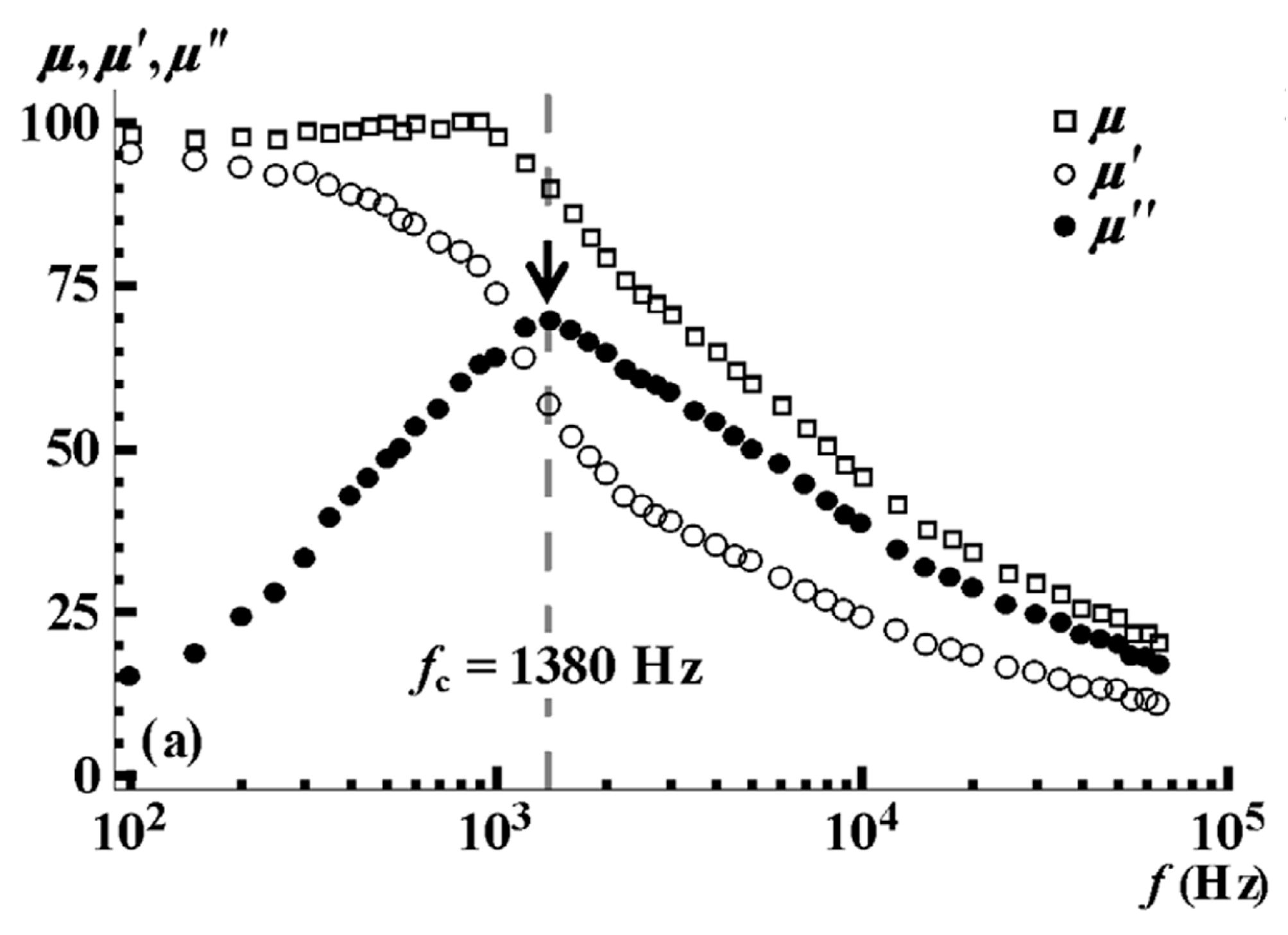
  62. Chowdary, K.; Majetich, S. Frequency-dependent magnetic permeability of Fe10Co90 nanocomposites. J. Phys. D Appl. Physics 2014, 47, 175001. [Google Scholar] [CrossRef]
  63. Zhou, W.; Zhong, X.; Sheng, K. High Temperature Stability and the Performance Degradation of SiC MOSFETs. IEEE Trans. Power Electron. 2013, 29, 2329–2337. [Google Scholar] [CrossRef]
Figure 1. Topology structure of FSBB.
Wevj 16 00315 g001
Figure 2. Single-mode control.
Wevj 16 00315 g002
Figure 3. Dual-mode controls. (a) Buck stage; (b) Boost stage.
Wevj 16 00315 g003
Figure 4. Simulation of single-mode and dual-mode inductor current waveforms. (a) Single-mode; (b) Dual-mode; Voltage and current waveforms of S3. (c) Single-mode; (d) Dual-mode.
Wevj 16 00315 g004
Figure 5. Principle of dead zone operation during mode switching. (a) Ideal duty cycle; (b) Actual duty cycle; (c) Ideal gain curve; (d) Actual gain curve.
Wevj 16 00315 g005
Figure 6. Operating principle of three-mode control. (a) Schematic diagram of duty cycle variation. (b) Schematic diagram of voltage gain.
Wevj 16 00315 g006
Figure 7. Schematic diagram of the four-mode control strategy. (a) Four-mode duty cycle variation. (b) Four-mode voltage gain curve.
Wevj 16 00315 g007
Figure 8. Graphic method for describing FSBB workspace. (a) Schematic diagram of the working area of the converter under ideal conditions. (b) Schematic diagram of voltage gain blind zone in actual situations.
Wevj 16 00315 g008
Figure 9. Graphical method to describe two different three-mode controls. (a) Simultaneous switching of paired transistors in three-mode control. (b) Fixing the duty cycle of either the Boost stage or the Buck stage.
Wevj 16 00315 g009
Figure 10. Three-mode smooth-switching control.
Wevj 16 00315 g010
Figure 11. Frequency-varying loop selection control strategy based on four-mode control.
Wevj 16 00315 g011
Figure 12. Control Block Diagram of Model Predictive Control. The design is based on the four-mode control.
Wevj 16 00315 g012
Figure 13. Waveform diagram under quadrilateral inductor current control.
Wevj 16 00315 g013
Figure 14. Equivalent circuit diagrams at different stages. (a) t0~t1 (b) t1~t2 (c) t2~t3 (d) t3~t4 (e) t4~t5 (f) t5~t6 (g) t6~t7 (h) t7~t8.
Wevj 16 00315 g014
Figure 15. 3-D lookup table method.
Wevj 16 00315 g015
Figure 16. 2-D lookup table method.
Wevj 16 00315 g016
Figure 17. Schematic diagram of magnetic core permeability changing with frequency.
Wevj 16 00315 g017
Figure 18. Schematic diagram of the influence of switch device parameters on temperature.
Wevj 16 00315 g018
Table 1. Relationship between variables.
ukd1d2M
0 < u < 1k > 1u0u
u = 1k = 1101
1 < u < 20 < k < 11u − 11/(2 − u)
Table 2. Comparison of different strategies.
StrategyModekAdvantageLimitation
Single-mode--The simplest controlHigh switch losses and large ripple in inductor current
Dual-modeBuck
Boost
k   >   1
k     1
Simple control and improved efficiencyExistence of boundary oscillation and poor dynamic performance
Three-modeBuck
Buck–Boost
Boost
k   >   1   +   Δ 2
1     Δ   1   <   k   <   1   +   Δ 2
k   <   1     Δ 1
Smooth transition The conduction loss in the intermediate mode is relatively high
Four-modeBuck
Extend Buck
Extend Boost
Boost
k   >   1   +   Δ 2
1   <   k   <   1   +   Δ 2
1     Δ 1   <   k   <   1
k   <   1     Δ 1
Smoothest transition and reduced rippleThe algorithm is complex and relies on high-precision sensors
Table 3. Summary of various optimization strategies.
Control MethodAdvantageLimitationReferences
Three-modeSimultaneous switching of paired transistorsSimple controlThe maximum amplitude of the duty cycle jump[28]
fixing the duty cycle of either the Boost stage or the Buck stageThe control is relatively simple, and the duty cycle jump is reducedIn specific cases, significant duty cycle jumps still exist[38]
Smoothly varying duty cycleThe three-mode control with the smoothest mode transitionThere is still room for improvement compared to the four-mode control[32]
Four-modeFixed duty cycleSmoother mode transitionLarge inductor current ripple[31]
Maximum duty cycleFrequency conversion controlHigh efficiency and good dynamic performanceThe control process is complex, and the system has a high computational load[35,36]
Model Predictive ControlGood dynamic performance and the ability to achieve fixed-frequency controlDependent on model design and sensor accuracy[42]
Table 4. Summary of various calculation methods.
Method of CalculationAdvantageLimitationReferences
lookup table3-DAvoid complex calculationsRequires a large amount of storage resources[47]
2-DDecoupling control variables[56]
Simplified Real-Time Calculation MethodFixed control variableSave costs and reduce computational complexityComplex EMI design[58]
Using a new mathematical modelFast dynamic response and reduced computational complexityRationality needs further verification through practice[61]
Approximate duty cycle phase shift methodFast dynamic responseIt will lead to a decrease in efficiency[54]
Disclaimer/Publisher’s Note: The statements, opinions and data contained in all publications are solely those of the individual author(s) and contributor(s) and not of MDPI and/or the editor(s). MDPI and/or the editor(s) disclaim responsibility for any injury to people or property resulting from any ideas, methods, instructions or products referred to in the content.

