Article

Research on Efficient Prediction and Suppression of Electromagnetic Interference in Electric Drive Systems

Deepal Automobile Technology Co., Ltd., Chongqing 400714, China
*
Author to whom correspondence should be addressed.
World Electr. Veh. J. 2025, 16(4), 201; https://doi.org/10.3390/wevj16040201
Submission received: 8 February 2025 / Revised: 21 March 2025 / Accepted: 25 March 2025 / Published: 1 April 2025

Abstract

:
Accurate prediction and efficient suppression of conducted electromagnetic interference(EMI) in electric drive systems(EDS) are achieved through an innovative technique proposed in this paper, leveraging a key path impedance characteristic model. The influence of critical components—namely; three-phase alternating current modules; motors; and insulated gate bipolar transistor drive parameters—on EMI is meticulously analyzed by establishing a current spectrum characteristic analysis model of the critical path impedance. This study calculates current characteristic curves under varying filter parameters for interference suppression, while voltage characteristic curves are computed based on a comprehensive electric drive system model. The mapping relationship between current and voltage spectrum characteristics is scrutinized, revealing a high consistency between the model’s current spectrum curves and the conducted interference voltage spectrum. This alignment enables precise prediction of risk frequency points. Moreover, the critical path impedance model remarkably enhances computational efficiency by 87.5%, thereby facilitating an efficient evaluation and design of EMI suppression in electric drive systems. The proposed technique effectively reconciles the incompatibility between accurate EMI prediction and efficient filter circuit design. Experimental results corroborate the technique’s accuracy and reliability. This method, validated through stringent testing, holds significant practical value and broad applicability, marking a substantial advancement in the field of electromagnetic compatibility for electric drive systems.

1. Introduction

The electric vehicle market has grown significantly in recent years, with global electric car sales reaching 14.1 million units in 2023, a 34% increase compared to 2022 [1]. This rapid growth highlights the increasing demand for more efficient drive systems that comply with electromagnetic interference regulations. With the widespread adoption of new energy vehicles, the EDS, as a core power unit, generates strong EMI due to the rapid switching of power semiconductor devices, which causes sharp increases in voltage and current change rates ( d v d t and d i d t ). This interference poses challenges to both the electromagnetic compatibility inside the vehicle and the electromagnetic safety outside the vehicle as required by regulations. EMI can significantly compromise the safety and performance of electronic systems within vehicles, as well as interfere with external devices, making it a critical concern for manufacturers and regulators. For instance, EMI can disrupt the operation of sensitive electronic components, affecting vehicle safety, performance, and user experience. Additionally, EMI can lead to inaccurate readings from sensors such as speed, position, temperature, and battery status, which can compromise safety-critical decisions [2]. In electric vehicles (EVs), the shift to higher voltage levels, such as from 400 V to 800 V, exacerbates EMI issues due to increased rates of voltage change ( d v d t ), which can further amplify these challenges [3].
In recent years, scholars and experts have conducted extensive research on the EMI characteristics and suppression technologies of EDS. In the existing literature, various studies have explored the EMI characteristics and modeling approaches for EDS. For instance, Reference [4] introduced a high-frequency motor modeling method that achieves relatively high precision. However, this method relies heavily on measured interference sources, leading to significant errors in medium and high frequency ranges. Reference [5] improved EMI prediction accuracy in high-frequency ranges by considering the switching characteristics of Silicon Carbide (SiC) devices, thereby addressing some of the limitations of Reference [4]. Reference [6] further enhanced modeling accuracy by using the resonant characteristics of common-mode and differential-mode impedance. Despite achieving higher precision, this method did not explore its impact on EMI prediction. In parallel, Reference [7] examined the influence of system layout on common-mode interference (referring to the unwanted electromagnetic noise that appears equally on all conductors relative to a common reference point, typically ground), providing valuable insights but failing to identify specific interference frequency bands. To address these gaps, Reference [8] proposed a universal power bus model for two types of shielding designs based on multi-conductor transmission line theory, offering a more comprehensive approach to understanding interference in complex systems. Finally, References [9,10,11] adopted a modular approach to precise modeling, establishing a simulation model for the integrated EDS. These studies focused on the impact of parasitic parameters on the system, providing detailed analyses that complement the broader findings of the previous references. Recent studies have focused on the simulation and optimization of EMI filters for high voltage gain DC-DC (Direct Current change to Direct Current) converters, which can provide valuable insights for the design of EMI filters in electric drive systems [12]. Reference [13], which proposed a SPICE equivalent circuit modeling method for electric vehicle motor drive systems based on port impedance measurement, and Reference [14] adopted a modular precise modeling approach to build a conducted electromagnetic interference prediction model for the electric drive system.
Despite these advancements, there remains a significant gap in the literature regarding the comprehensive analysis and optimization of EMI suppression in multi-in-one electric drive systems. Current research has primarily focused on the individual effects of filters or specific parameters (such as Insulated Gate Bipolar Transistor (IGBT) parasitic capacitance, cable types, etc.) on EMI in specific EDS. However, these studies lack a comprehensive analysis of full-frequency-band factors and are not readily applicable to other types of EDS. This study aims to address these gaps by proposing a novel prediction technique for conducted emission intensity based on key-path impedance characteristics. This method not only improves the efficiency of filter circuit design but also accurately predicts EMI emission intensity, offering significant practical value and broad applicability.
The main scientific contributions of this work are as follows: Firstly, development of a novel prediction technique for conducted emission intensity in EDS based on key-path impedance characteristics. Secondly, optimization of filter parameters using the proposed method, ensuring compliance with stringent Electromagnetic Compatibility (EMC) standards. Last but not least, experimental validation of the proposed technique, demonstrating high consistency between simulation and measurement results.

2. Impact of Modules on EMI in Multi-in-One EDS

The standard for conducting interference simulation analysis of the EDS is the international standard CISPR 25–2016 [15]. The CISPR25 standard classifies limit values into five levels (Level 1 to Level 5); Level 3 is widely accepted and used in the automotive industry. Therefore, this study adopts Level 3 as the assessment standard for evaluating the conducted emission interference voltage of the electric drive system.

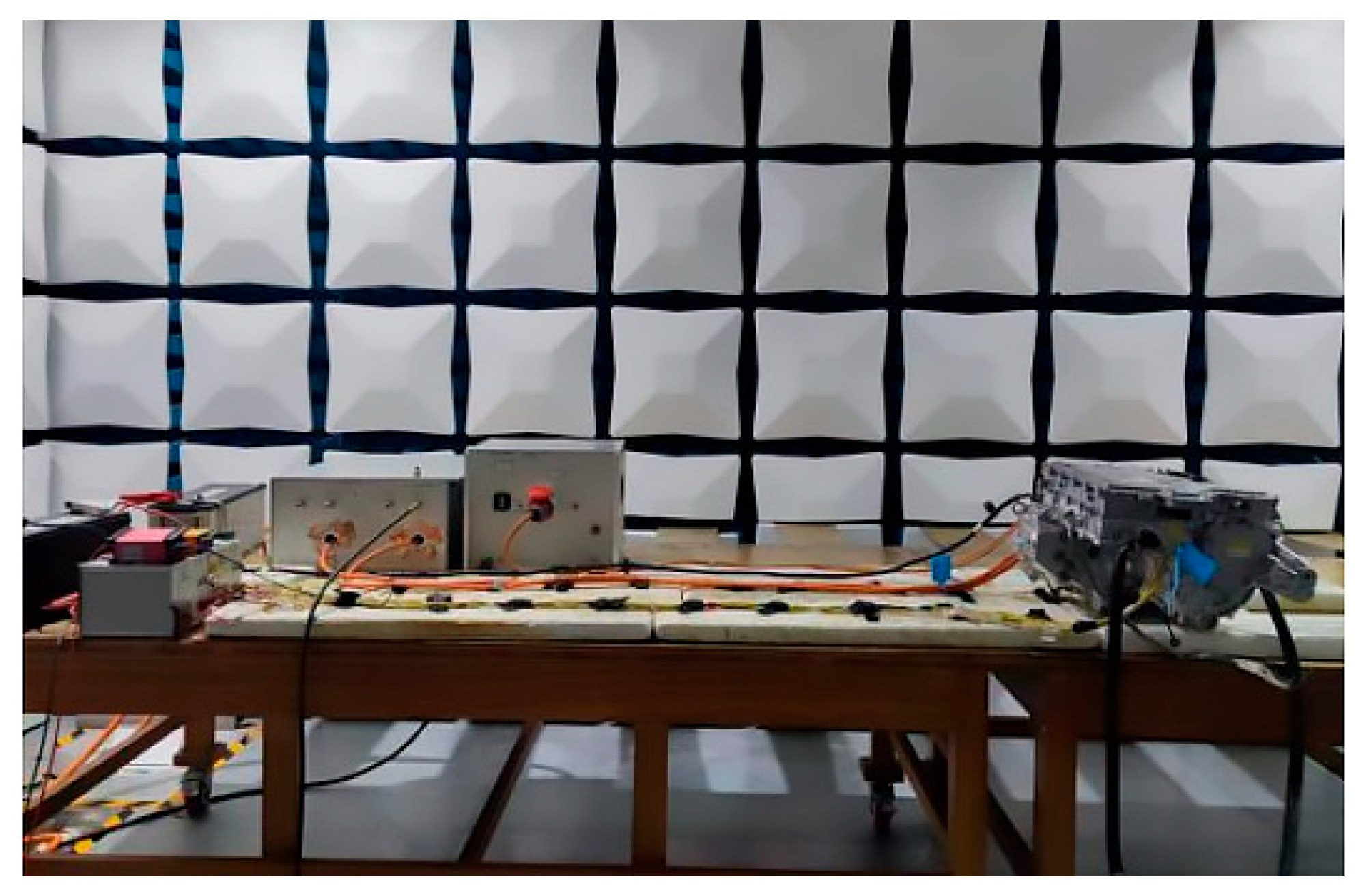
2.1. An Integrated Electrified Power Train Conducted Emission Simulation Model

To perform the simulation of conducted interference voltage in the EDS, an integrated simulation model for the multi-in-one EDS is established, as shown in Figure 1. The simulation results of the conducted interference voltage obtained from this model exhibit good consistency with the measured data, thereby validating the reliability of the model [1]. Based on this model, the conducted emission voltage without filtering is calculated, as depicted in Figure 2.
Figure 2 illustrates the conducted interference voltage of the multi-in-one EDS without filtering measures (blue curve) and the standard limit curve for Level 3 components (brown curve). The unfiltered system significantly exceeds the regulatory limits in the frequency bands of 530 kHz–1.8 MHz and 5.9–6.3 MHz, indicating a failure to meet EMC requirements. To ensure that the electric drive system meets the design standards, it is necessary to optimize and improve the parameters of the EDS for the frequency bands that exceed the limits, thereby reducing the conducted interference voltage below the Level 3 limit requirements.
EMI in multi-in-one electric drive systems is influenced by various key modules, including high-voltage DC cables, filtering circuits, IGBT, AC (Alternating Current) modules, motors, and drive signals. However, existing research has extensively studied the impact of high-voltage DC and drive signals on the interference voltage spectrum [5,8]. In contrast, studies on IGBT drive parameters, AC modules, and motors have primarily focused on the precise modeling of each individual module, lacking research on the interference impact of these modules across different frequency bands within the EDS. Each module in the EDS affects the conducted interference voltage spectrum in different ways. Understanding their impact within the frequency bands of interest in the electric drive system is of great guiding significance for solving the problem of exceeding the regulatory limits and providing effective electromagnetic interference suppression measures. Therefore, the following sections will analyze the impact of IGBT drive parameters, AC modules, and motors on the conducted interference voltage spectrum

2.2. Impact of Three-Phase AC Module

The three-phase AC module can influence EMI due to the interaction between cable impedance and semiconductor switching transients. This effect can be observed through the spectral interference curves. The three-phase AC module is a key component connecting the inverter and the motor, and it is also part of the conducted emission interference path in the EDS. However, its impact on the frequency range and extent of interference has not yet been analyzed in detail. Therefore, this paper analyzes the influence of the three-phase bus based on a complete EDS model. The specific analysis is as follows: 1. For the EDS without filtering measures, the simulation results of adding and removing the three-phase AC bus are shown in Figure 3a. In the EDS with Capacitor-Inductance-Capacitor-Capacitor (CLCC) filtering measures, the simulation results of the impact of adding and removing the three-phase bus on the conducted interference voltage spectrum (referring to the frequency distribution of voltage levels resulting from EMI that is conducted through power cables) are shown in Figure 3b.
Figure 2 demonstrates that adding the three-phase AC module increases interference in the 150 kHz–12 MHz range without a filter, and reduces interference across the entire frequency band with a filter, especially in the 12 MHz–30 MHz range, with a reduction of up to 5 dBμV. This suggests that AC bus design can directly influence the electromagnetic compatibility of the system. Additionally, the parameters of the three-phase bus interact with other system parameters, causing frequency shifts (refer to the changes in the frequency of resonances due to variations in system parameters) in the resonance points near 10 MHz. Therefore, the impact of the three-phase bus cannot be ignored in the comprehensive EMI analysis of the EDS.

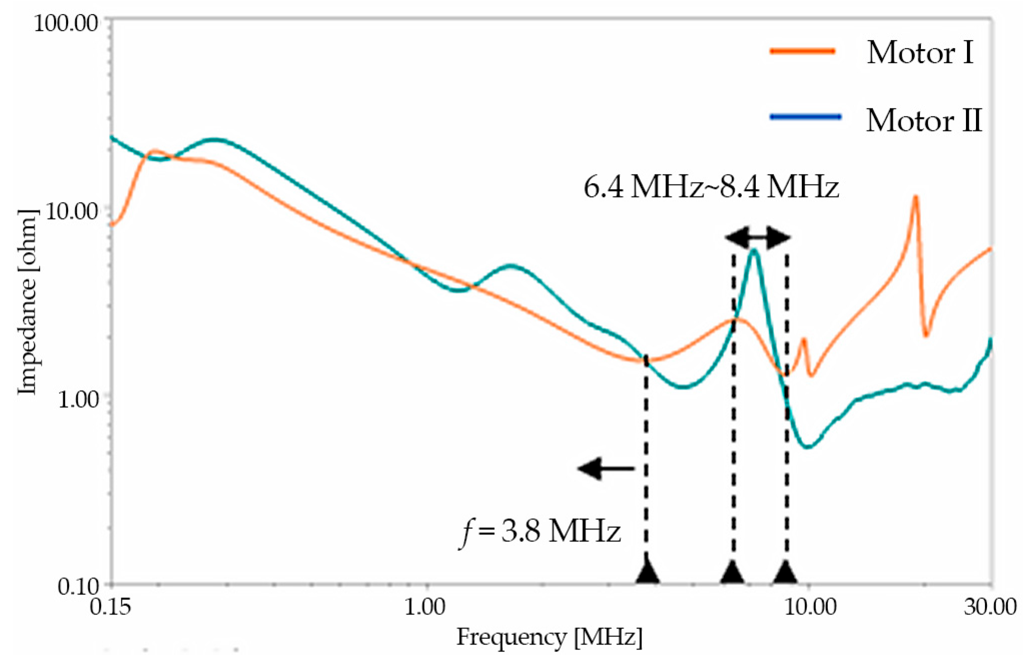
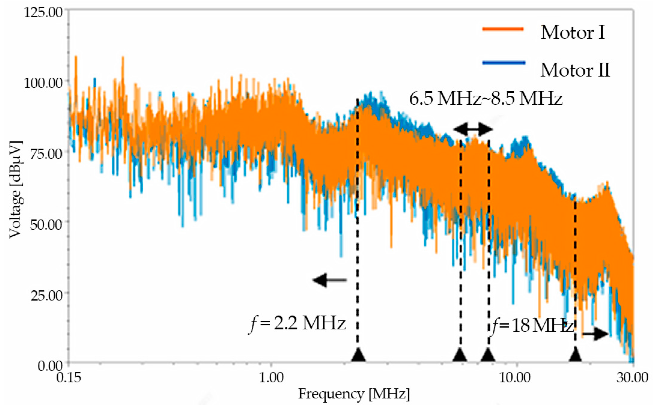
2.3. Impact of Motor Impedance on EMI in EDS

Current research has extensively explored the modeling of motor impedance, but there is limited analysis on how different motors affect the conducted interference voltage spectrum of EDS. In this study, we used an impedance analyzer to measure the impedance characteristics of two different motors (as shown in Figure 4) and established their impedance models using vector fitting techniques. Based on these models, we calculated the conducted interference voltage of the EDS (as shown in Figure 5).
The analysis of Figure 4 and Figure 5 demonstrates that the impedance characteristics of the two motors and the conducted interference voltage spectrum exhibit distinct differences within the frequency range of 2.2 MHz to 18 MHz. Motor 2 shows higher impedance than Motor 1 in the frequency bands of 150 kHz to 3.8 MHz and 6.4 MHz to 8.4 MHz, whereas Motor 1 exhibits higher impedance in other frequency ranges. In terms of conducted interference voltage, the two motors have comparable levels in the 150 kHz to 2.2 MHz and 18 MHz to 30 MHz, while Motor 2 displays lower voltage in the 6.5 MHz to 8.5 MHz band. These findings suggest a correlation between motor impedance and conducted interference voltage, particularly in the 2 MHz to 30 MHz range. Specifically, higher motor impedance is associated with reduced interference voltage. Motor I has resonant peaks at 6.6 MHz, 9.7 MHz, and 19 MHz, with the 9.7 MHz peak attributed to the combined effects of heat sink pad capacitance, AC bus, and the motor itself. In contrast, Motor II has resonant peaks at 1.7 MHz and 7.2 MHz, but no clear correlation with the interference voltage spectrum is observed due to the masking effect of the filter’s low-impedance path. In summary, the impedance characteristics of the motor have a direct influence on the high-frequency components of the conducted interference voltage. Accurate impedance modeling is therefore crucial for predicting conducted emissions in EDS.

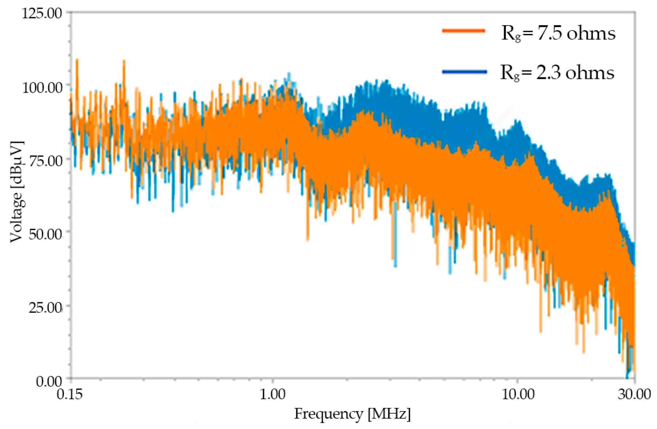
2.4. Analysis of the Impact of IGBT Drive Resistance

Some researchers explored the impact of IGBT internal parameters on EMI [16,17]. However, studies on the influence of external parameters, such as gate drive resistance, on the EMI of EDS are limited. Specifically, the frequency range and extent of EMI caused by drive resistance have not been fully investigated. Existing IGBT switch models are primarily based on double-pulse test data, which is effective for analyzing and modeling IGBT switching characteristics. However, the actual gate drive resistance in EDS often differs from the values used in double-pulse tests. In this study, we compared the effects of two different Gate Drive Resistances (Rg), 7.5 Ω and 2.3 Ω, on the conducted interference voltage of the system (as shown in Figure 6).
The simulation results indicate that increasing the gate drive resistance from 2.3 Ω to 7.5 Ω significantly reduces the conducted interference voltage in the frequency range of 1.3 MHz to 30 MHz. This is because a higher drive resistance slows down the switching speed, reduces the rise time, lowers the interference voltage break-point frequency, and decreases the L d i d t , which is consistent with theoretical analysis. This demonstrates that drive parameters directly influence the slope of the interference voltage, thereby affecting the strength of mid- to high-frequency interference.
The analysis of key modules in the EDS indicates that EMI is strongly influenced by motor impedance and IGBT drive settings. However, the impact of the AC module and motor impedance on the frequency bands that exceed the standard limits in this study is relatively minor. While increasing the gate resistor can reduce the interference voltage in the frequency band of 5.9–6.2 MHz, it also decreases switching efficiency and increases switching losses of the device. These modules are therefore unable to optimize the frequency bands that exceed the standard limits as discussed in Section 2.1. Consequently, to bring the conducted voltage in Section 2.1 into compliance with Level 3 limits, the next section will employ filters to suppress interference in specific frequency bands.

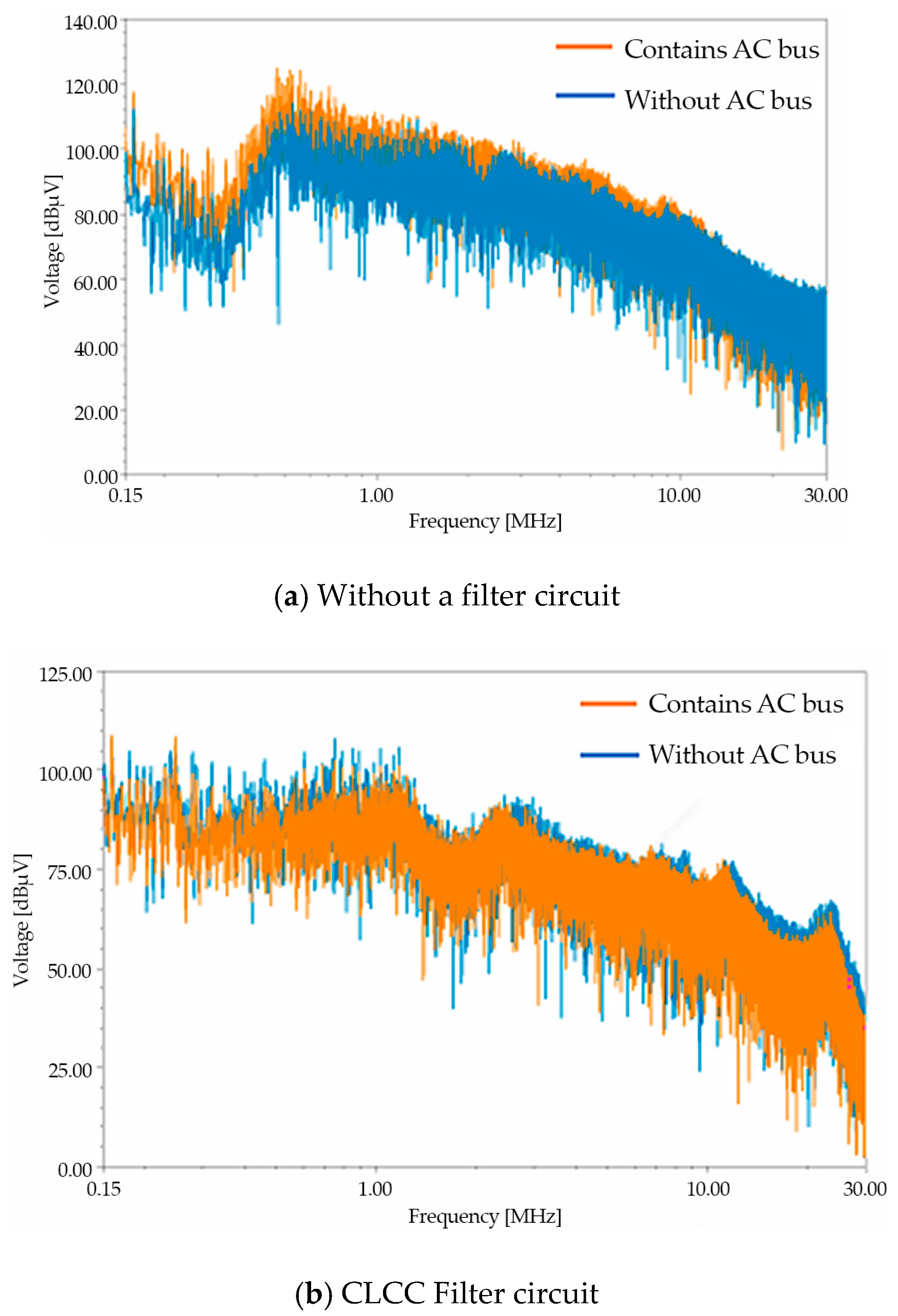
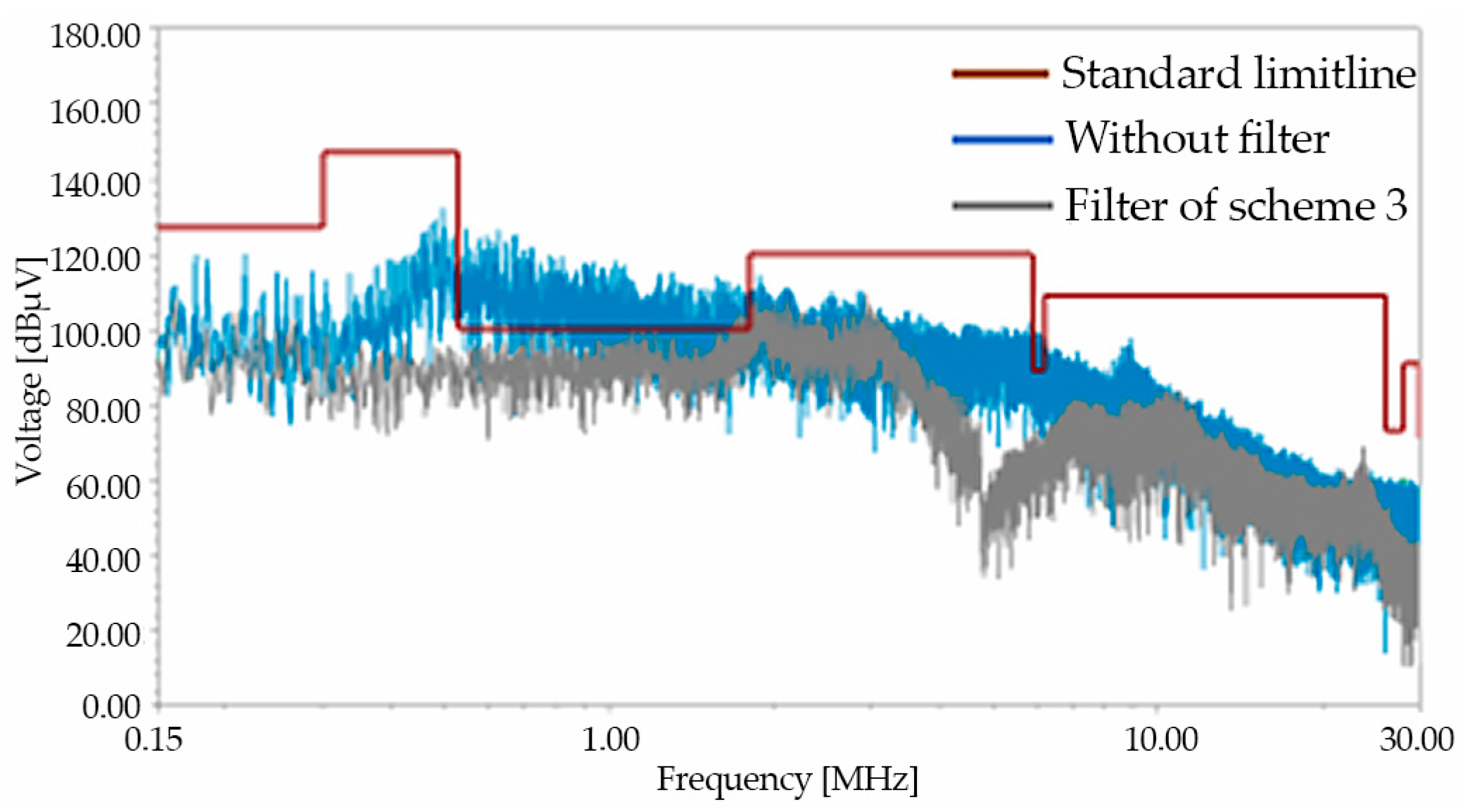
3. Impact of Filters on EMI in EDS

Filters work by reducing conducted interference by attenuating specific frequency ranges. EMI filtering is essential for ensuring electromagnetic compatibility in EDS. However, selecting and designing effective filters is challenging due to the complexity of interference paths and interactions between system components. The optimization of passive filter components through active filtering techniques has been explored in inverters, offering a potential approach for improving EMI suppression in electric drive systems [18]. This section analyzes the impact of filters on EMI and proposes an impedance-based optimization approach.

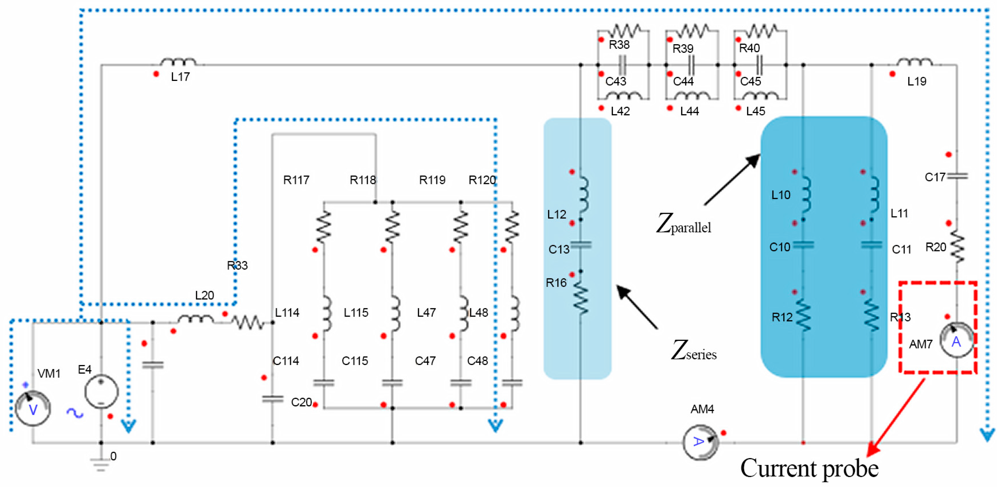
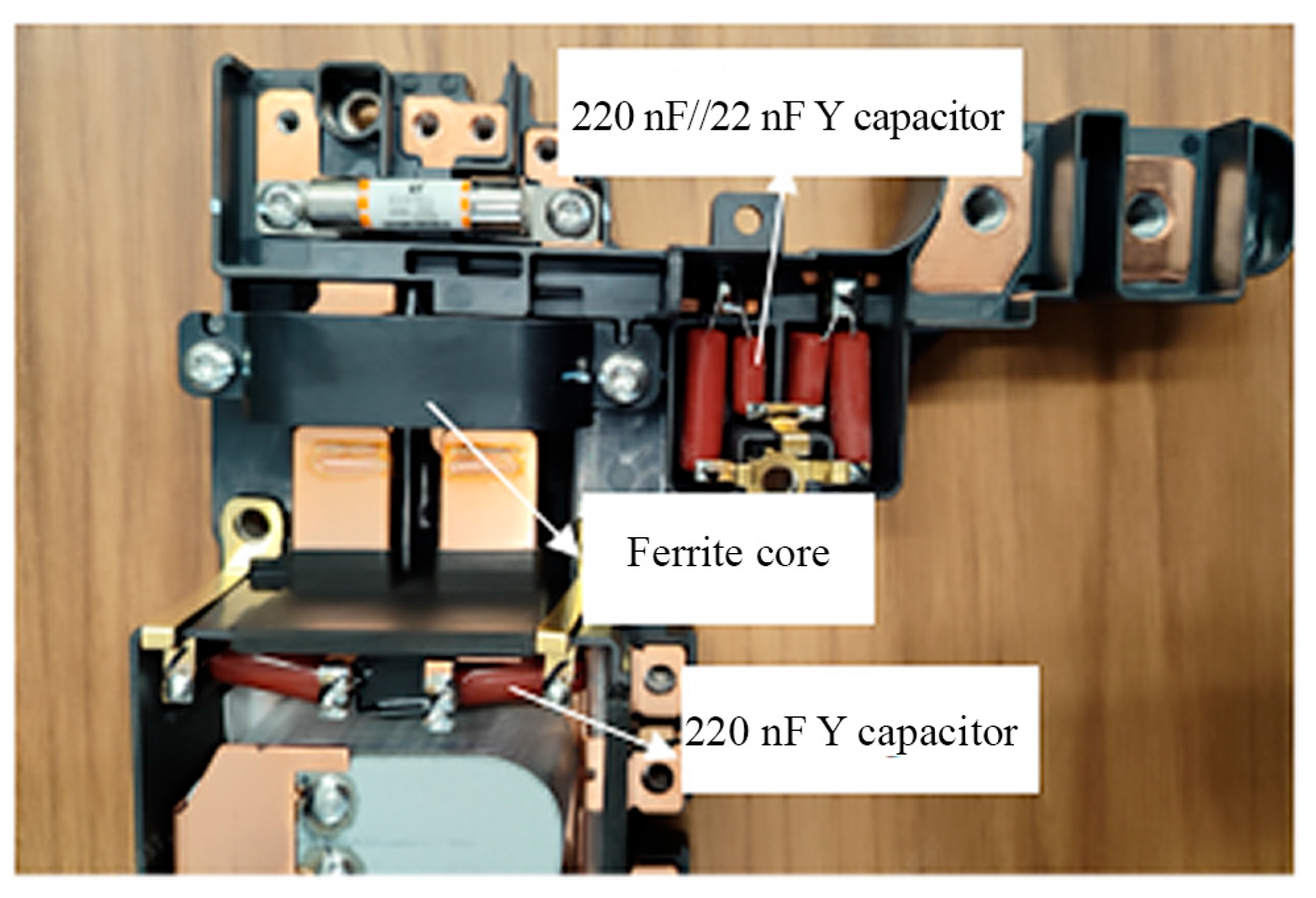
3.1. Simulation Analysis of Filter Impedance Characteristics in EDS Based on Critical Paths

The voltage at the receiver end of the receiving device is significantly influenced by the impedance and parasitic parameters of each module along the conduction interference path of the EDS. To enhance model versatility and filtering circuit design efficiency, a prediction technique based on key-path impedance characteristics is proposed to approximate the conducted emission intensity. The technique is implemented using a filtering architecture based on the common-mode choke and capacitor combination (CLCC). By analyzing the key paths of conduction emission in the EDS, three main paths are identified:
(1) The interference source travels from the IGBT through the heat sink capacitance and returns to the interference source;
(2) The interference source travels from the IGBT through the three-phase bus, the motor impedance, and returns to the IGBT;
(3) The interference source travels from the IGBT through the filtering circuit, the LISN, and returns to the IGBT.
An equivalent analysis model of the key-loop impedance characteristics of the EDS, including the filtering circuit, is constructed, as shown in Figure 7. This model ensures that the current characteristics of the branch with a 50 Ω load are positively correlated with the voltage characteristics of the conducted emission interference in the EDS. By controlling and optimizing the filter parameters in the key path impedance characteristic equivalent model, the proposed technique enables risk prediction of the conducted emission interference voltage and its suppression. The key parameter for evaluating the effectiveness of the filter parameters in interference suppression is the current characteristic curve measured by the probe in the 50 Ω load branch.
The voltage characteristics at the receiver end can be equivalently obtained by calculating the current in the 50 ohm resistor branch at the LISN end. Depending on the filter configuration, different frequency bands may be impacted. Below, we analyze three distinct filter configurations and their effectiveness in reducing EMI. In this model, three different parameter combinations of capacitors are designed in this paper: 220 nF//220 nF//22 nF, 220 nF//220 nF//1 nF, and 220 nF//22 nF//1 nF. For the convenience of subsequent analysis, the three sets of filter parameter combinations are defined as follows: 220 nF//220 nF//22 nF as Scheme 1220 nF//220 nF//1 nF as Scheme 2220 nF//22 nF//1 nF as Scheme 3.
Where, Current probe: Used to measure the current characteristic curves in the 50 Ω load branch.
Zseries: Represents a single branch of Y-capacitors with parasitic parameters, located near the IGBT end, with a value of 220 nF.
Zparallel: Represents a composite branch consisting of two parallel Y-capacitors (such as 220 nF//22 nF, 220 nF//1 nF and 22 nF//1 nF) with parasitic parameters, located near the power supply end.
Zseries and Zparallel are connected through a common-mode choke and then paralleled together to form the overall filter network. By substituting the three sets of filter parameters from Zseries and Zparallel into the impedance equivalent model shown in Figure 7, frequency-domain calculations are performed to obtain the characteristic curves in the frequency range of 0.15 MHz to 50 MHz, as received by the current probe. The results are illustrated in Figure 8.
As shown in Figure 8, the complete Y-capacitor combination in the EDS is characterized by a configuration of Scheme 1. The corresponding current characteristic curve is illustrated as the blue curve. The impedance characteristic equivalent model yields three resonant frequency points, which align with the valley points in the current characteristic curve. Concurrently, three resonant peak points are observed, which are identified as the risk points predicted by the equivalent model proposed in this study. Similarly, for the Y-capacitor combination of Scheme 2 and Scheme 3, the current characteristic curves are represented by the green and gray curves, respectively. Through simulation analysis of the impedance characteristics of the three sets of filter parameters, the following observations are made:
The 220 nF Y-capacitor in the single branch of Zseries generates resonant points a1, b1, and c1, with corresponding resonant frequencies fa1 = fb1 = fc1 = 900 kHz. These capacitors also generate resonant risk points p1, k1, and j1, with corresponding frequencies of 830 kHz.
The 220 nF Y-capacitor in Zparallel generates resonant points b2 and a2, with corresponding resonant frequencies fb2 = 1.5 MHz and fa2 = 1.9 MHz. The interaction between the 220 nF Y-capacitor in Zparallel and the 220 nF Y-capacitor in Zseries results in resonant risk points k2 and p2, with corresponding frequencies of 1.2 MHz and 1.3 MHz, respectively. The frequency differences observed are attributed to the variations in parasitic parameters between the 220 nF in parallel with the 22 nF Y-capacitor and the 220 nF in parallel with the 1 nF Y-capacitor.
The 22 nF Y-capacitor in Zparallel generates resonant points c2 and a3, with corresponding resonant frequencies fc2 = 4.8 MHz and fa3 = 7.8 MHz. The interaction between the 220 nF Y-capacitor in Zseries and the 22 nF Y-capacitor in Zparallel results in resonant risk point j2. Additionally, the interaction between the 220 nF Y-capacitor and the 22 nF Y-capacitor in Zparallel results in resonant risk point p3, with corresponding frequencies of 3.6 MHz and 5.7 MHz, respectively. The frequency differences are attributed to the variations in parasitic parameters between the 220 nF Y-capacitor in Zseries and the 220 nF Y-capacitor in Zparallel.
The 1 nF Y-capacitor in Zparallel generates resonant points b3 and c3, with corresponding resonant frequencies fb3 = fc3 = 33 MHz. The interaction between the 220 nF Y-capacitor in Zparallel and the 1 nF Y-capacitor or between the 22 nF Y-capacitor and the 1 nF Y-capacitor in Zparallel, results in resonant risk point k3 (j3), with a corresponding frequency of 24.3 MHz.
Where a1, a2, a3, b1, b2, b3, c1, c2, and c3 represent resonant points, while fa1, fa2, fa3, fb1, fb2, fb3, fc1, fc2, and fc3 represent the corresponding resonance frequencies of these points, p1, p2, p3, k1, k2, k3, j1, j2, and j3 indicate the resonance risk points, that is, the points that may cause the conducted interference voltage of the system to exceed the standard limit curve.
The simulation analysis results reveal that while filter circuits are effective in suppressing interference within specific frequency bands, they may also introduce non-ideal resonant points, thereby posing additional risks to the system. The design of filter parameters is thus crucial, aiming to minimize the interference intensity at non-compliant frequency points while mitigating the risks associated with non-ideal resonant points. The interference suppression effects of the three filter parameter combinations were analyzed in detail for the frequency bands of concern in the EDS, specifically within the non-compliant frequency ranges of 0.53 MHz to 1.8 MHz and 5.9 MHz to 6.2 MHz. The results are as follows:
(1) The 220 nF capacitor generates non-ideal resonant points at 1.2 MHz and 1.3 MHz, which fall within the non-compliant frequency range of the unfiltered system, thereby posing a risk of exceeding the emission limits.
(2) The 22 nF capacitor generates non-ideal resonant points at 3.6 MHz and 5.7 MHz, which lie outside the non-compliant frequency range of the unfiltered system, indicating that it does not introduce additional risks of exceeding the limits.
(3) The 1 nF capacitor generates a non-ideal resonant point at 24.3 MHz, which is well above the non-compliant frequency range and does not lead to excessive conducted interference voltage.
Based on the impedance characteristics analysis in Section 3.1, we explore how to adjust filter parameters to maximize EMI attenuation. By integrating the impedance model calculations proposed in this paper, we identify the filter parameter combination of Scheme 3 as an optimal solution.
In Section 3.2, we aim to validate two critical aspects: first, whether the key impedance models in Section 3.1 can accurately assess the risk of conducted interference voltage and second, whether Scheme 3 effectively suppresses interference voltage in the risk frequency bands. To achieve this, we perform a comprehensive calculation of the conducted interference voltage using the three sets of filter parameters from Section 3.1. A detailed analysis of the voltage spectral characteristics will confirm the relationship between the current spectral curves in Section 3.1 and Section 3.2 and verify Scheme 3 as the optimal solution for interference suppression in the EDS.

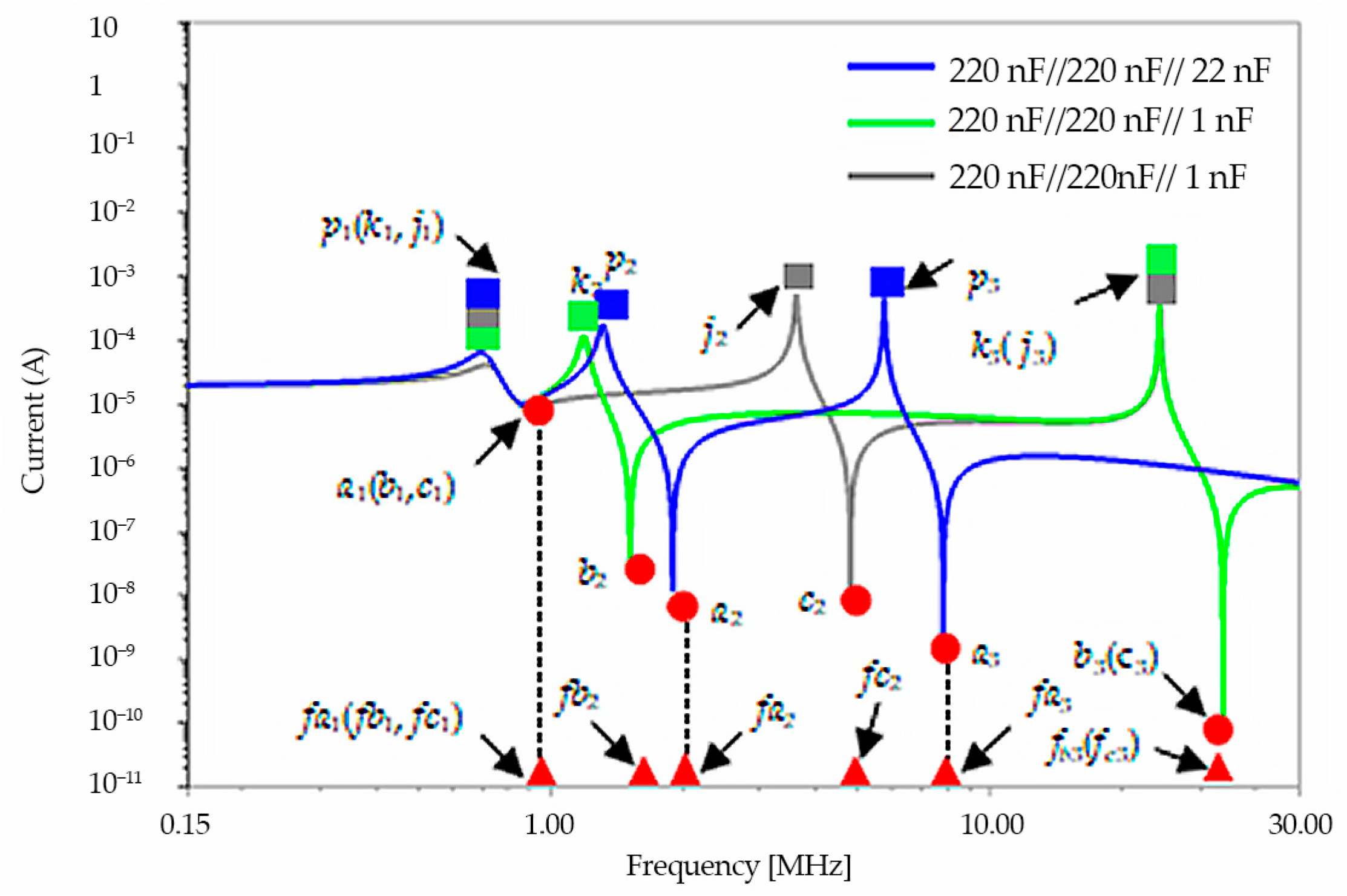
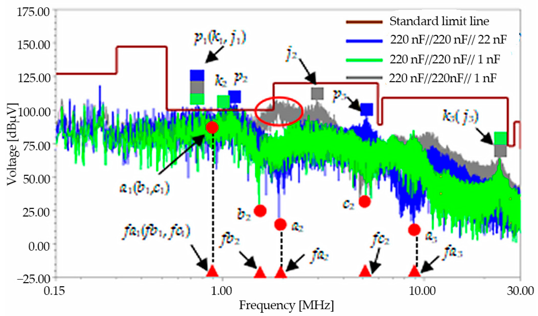
3.2. Filter Parameter Optimization Based on Electric Drive System Model

Hybrid optimization methods for common mode chokes in EMI filter design have been proposed, which could be beneficial for enhancing the performance of EMI filters in EDS [19]. A mathematical design approach to volumetric optimization of EMI filters and modeling of common mode noise sources has been presented, which could be applied to the optimization of EMI filters in electric drive systems [20].
In this section, the accuracy and reliability of the prediction technique are further verified, and its value and limitations in practical applications are explored. To verify whether there is a direct mapping relationship between the current spectrum curve of the characteristic impedance model and the conducted emission voltage of the complete EDS model, the three sets of filter parameters were respectively substituted into the complete EDS conducted emission simulation model for calculation, and the simulation results are shown in Figure 9.
As shown in Figure 9, the corresponding conducted emission voltage spectral curve of Scheme 1 is illustrated as the blue curve. for the Y-capacitor combination of Scheme 2 and Scheme 3, the voltage spectral curves are represented by the green and gray curves, respectively.Resonance peaks are observed at 1.1 MHz and 1.16 MHz for both Scheme 1 and Scheme 2. The simulation results indicate that these frequencies pose a risk of exceeding the regulatory limits. Notably, Figure 7 reveals that these resonance frequencies closely correspond to the risk frequencies k2 (1.2 MHz) and p2 (1.3 MHz).
For Scheme 1 and Scheme 3, resonance peaks are also observed at 3 MHz, 5.2 MHz, and 23.9 MHz. The simulation results show that these frequencies do not pose a risk of exceeding the regulatory limits. These resonance frequencies also closely correspond to the risk frequencies j2 (3.6 MHz), p3 (5.7 MHz), and k3 (j3) (24.3 MHz) identified in Figure 7. However, Scheme 3 exhibits a risk of exceeding the limits in the frequency range of 1.7–1.8 MHz. This frequency band is considered a simulation error and can be disregarded, as demonstrated in the comparison between simulation and experimental results in Section 4.
Given the identified critical frequency bands of 0.53–1.8 MHz and 5.9–6.2 MHz, this section concludes that Scheme 3 is capable of satisfying the conducted emission limit requirements. This is supported by the analysis from Section 3.1, which shows that the current spectrum curves, calculated using an interference suppression effect evaluation model based on the impedance characteristics of the critical path, closely match the conducted emission interference voltage spectrum curves of the Electric Drive Systems (EDS). The consistency between the conclusions drawn from both models validates the accuracy of our approach.
Figure 10 illustrates the effectiveness of Scheme 3 by incorporating its filter parameters into the conducted interference voltage simulation model depicted in Figure 1. The simulation data were compared against the interference voltage levels observed without filtering. The introduction of Scheme 3 significantly reduces the interference voltage levels within the critical frequency bands where the unfiltered system exceeds regulatory limits. Specifically, in the 0.53–1.8 MHz band, the interference voltage is reduced by up to 28 dBμV, and in the 5.9–6.2 MHz band, the reduction is as much as 26 dBμV. These results underscore the filter’s effectiveness in not only diminishing overall EMI but also shifting resonance frequencies to less critical regions, thereby enhancing the system’s electromagnetic compatibility.
Focusing on these identified risk frequency bands is pivotal for the compliance assessment of EDS. They correspond to the critical frequency ranges where conducted emission levels are most likely to exceed regulatory limits. By concentrating on these bands, we can more effectively evaluate how different filter parameter combinations perform in suppressing interference. Notably, our analysis indicates that the filter parameter combination of Scheme 3 effectively mitigates interference within these critical bands, ensuring the system meets conducted emission limit requirements. This targeted approach enhances the precision of our compliance assessment and optimizes filter design for practical applications.
The proposed method enables efficient and quantitative assessment of conducted interference voltage suppression in the EDS under various filter parameters. The analysis demonstrated that filters effectively suppress EMI but may introduce unwanted resonances. Impedance modeling allows predicting these risk frequencies and adjusting filter parameters to minimize interference. The computational efficiency is enhanced by an approximate equivalent model based on the critical path impedance, which excludes IGBT drive signals and active devices, consisting only of passive components. This model, highly adaptable to the key conduction path, closely matches the complete EMI calculation results. It can be effectively used for optimizing high-voltage filter parameters. Notably, the computation time for a single set of data using the proposed critical path impedance model is approximately 30 min, whereas the existing technology (complete electric drive system model) requires 4 h. This represents an 87.5% improvement in computational efficiency, significantly reducing the time required for filter design and optimization. The conclusions of this section support the proposed methodology for EMI optimization in the electric drive system.

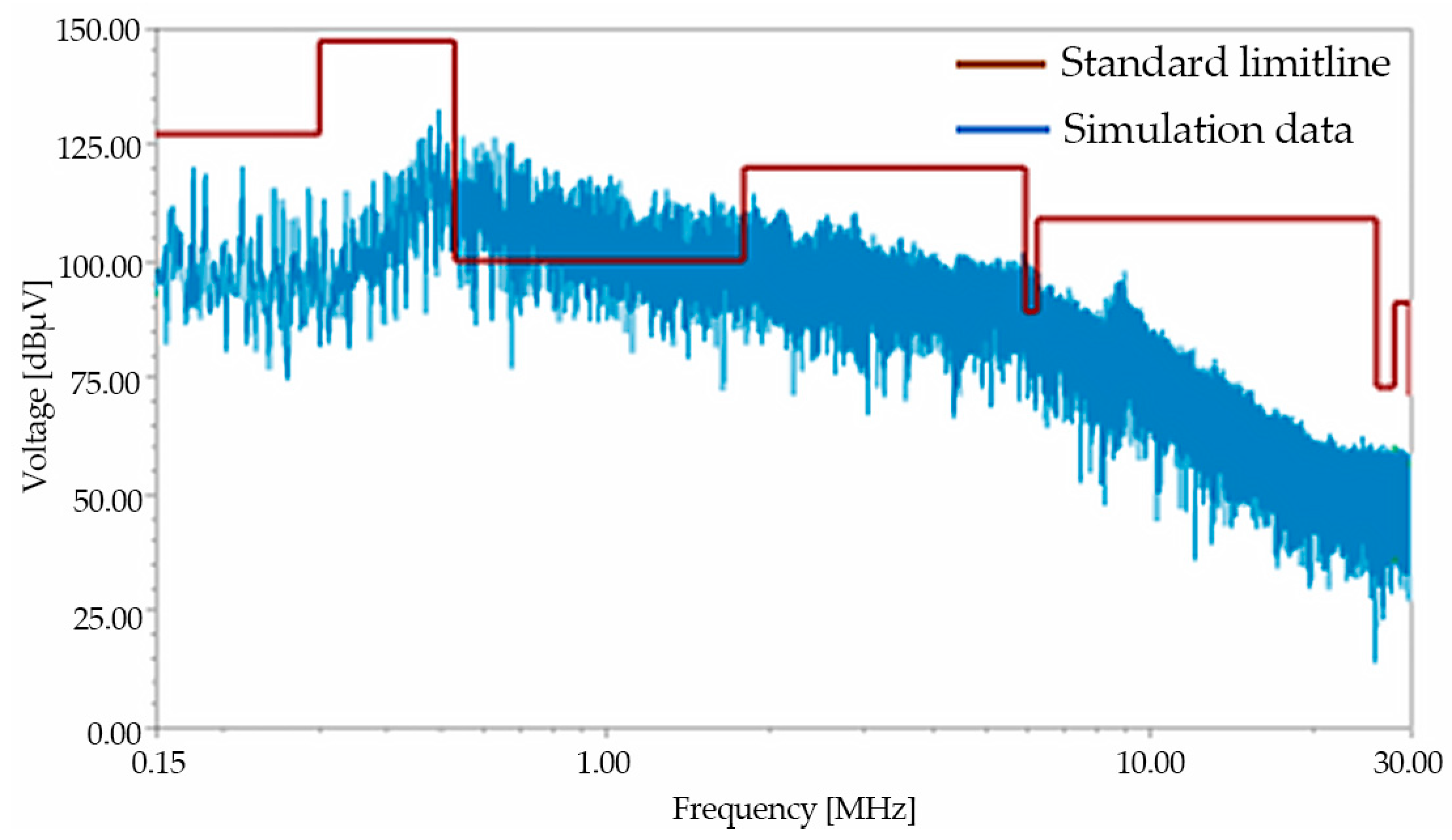
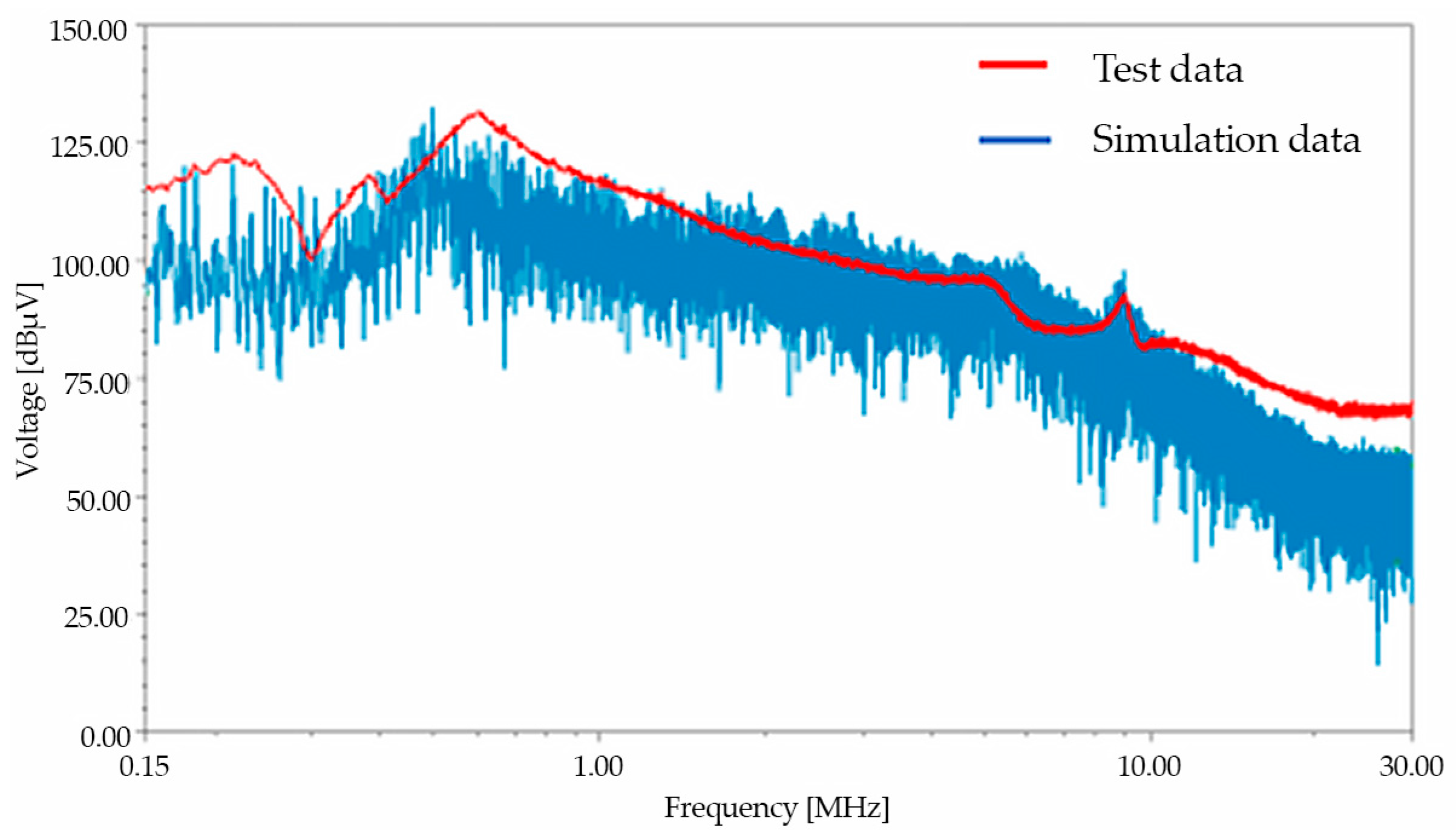
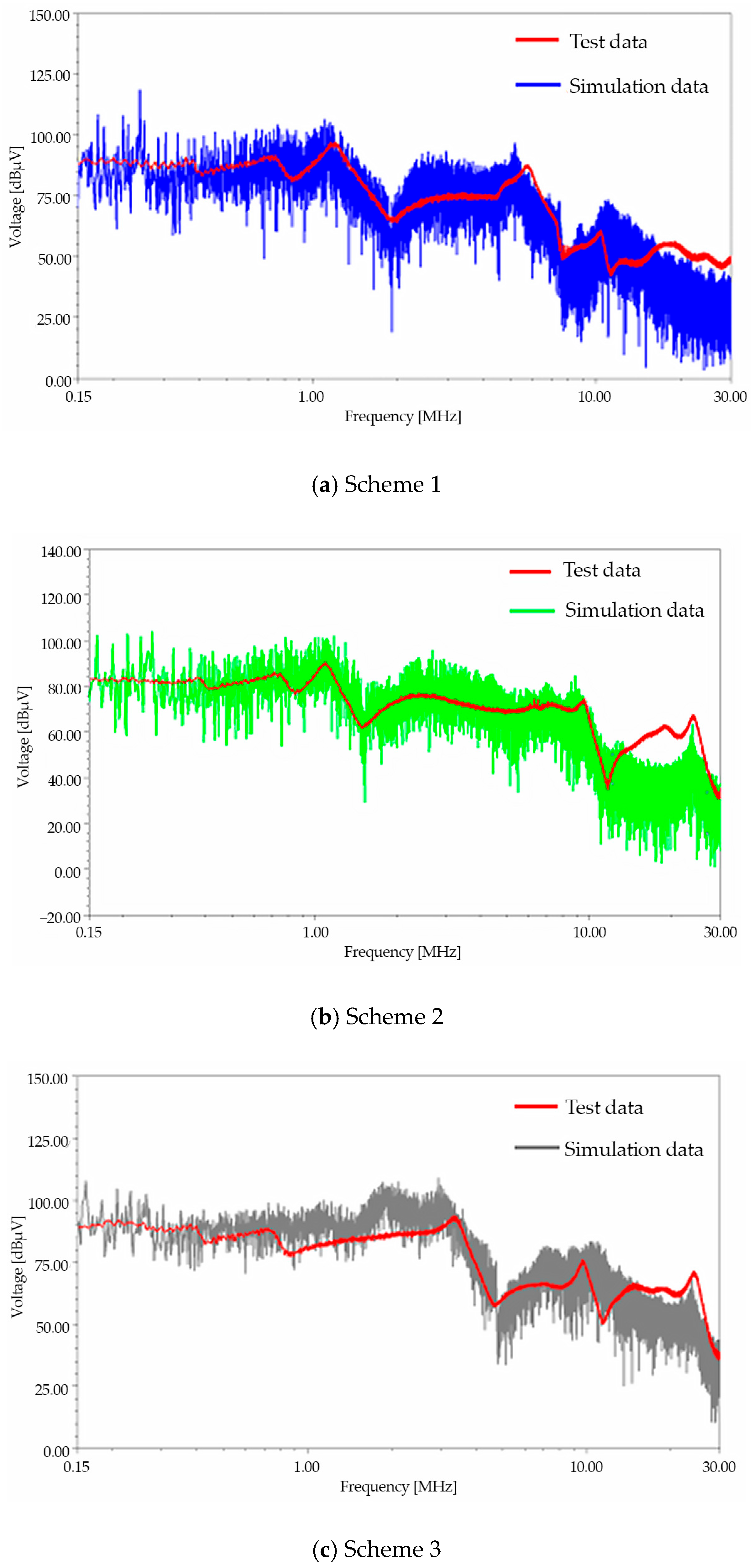
4. Comparison Between Simulation and Measurement

The design and control of high voltage gain DC-DC converters for CubeSat propulsion have been investigated, which may provide useful references for the simulation and measurement of EMI in electric drive systems [21]. To verify the reliability of the prediction model for the conducted emission intensity of EDS based on the impedance characteristics of key paths, a test for the multi-in-one EDS was set up at a professional testing institution. The test layout is shown in Figure 11, and the physical structure of the filter architecture is shown in Figure 12.
Based on the test, emission tests were completed under high-voltage conditions without filtering and with three different filter parameters. The filter circuit is located between the IGBT port and the DC bus port, using a CLCC capacitor-bead-capacitor filter architecture. Due to space limitations, the analysis mainly focuses on three combinations of Y capacitor filter parameters: Scheme 1, Scheme 2, and Scheme 3. Four sets of measured conducted emission interference voltage spectrum data were obtained and compared with the simulated voltage under the same conditions, as shown in Figure 13 and Figure 14a–c.
As shown in Figure 11, the simulation and measured data of conducted interference voltage for the EDS without filtering are highly consistent, with frequency errors of risk points and resonant points less than 1 MHz and amplitude errors less than 3 dBμV. Together with the relationship between the simulation curves and the limit standards shown in Figure 5, this verifies that the model established in this paper can accurately predict the conducted interference risk of the EDS.
As shown in Figure 14, the simulation and experimental curves of conducted emissions for the EDS with different filter parameters exhibit a high degree of consistency in trend. The simulation data accurately correspond to the risk resonance frequencies and their respective amplitudes observed in the experimental measurements, thereby achieving a high level of prediction accuracy. Additionally, the discrepancy where the simulation results exceed the experimental values in the frequency range of 1.3–2 MHz for Scheme 3 is attributed to simulation errors not related to the filter parameters.
In Section 3, we conducted a detailed analysis of the emission risk frequency bands of the EDS and identified 0.53 MHz–1.8 MHz and 5.9 MHz–6.2 MHz as the critical risk frequency bands. Through simulation and experimental validation, we demonstrated that Scheme 3 meets the conducted emission limit requirements. This finding establishes a direct mapping relationship between the current spectrum curve based on the impedance characteristics of the critical path and the conducted emission interference voltage spectrum curve of the EDS. This not only verifies the accuracy of the simulation model but also proves the effectiveness and applicability of the prediction method based on the impedance characteristics model of the critical path in practical applications.
In summary, the proposed method identifies critical risk frequency bands and quantitatively assesses the suppression of conducted interference voltage through a combination of simulation and experimental validation. The high consistency between the simulation and measurement data without filtering verifies the model’s effectiveness. The introduction of different sets of high-voltage filter parameters and the corresponding simulation and bench testing further demonstrate the model’s ability to accurately predict risk frequency points and amplitude levels. This consistency across various filter settings indicates that the proposed method can efficiently design high-voltage filter circuits and quantitatively assess the suppression effect of interference voltage. Although the current study is based on a specific EDS, the method is applicable for predicting conducted interference voltage risks and assessing suppression effects in other EDS. Future work will involve validating the model with different EDS to determine the generalizability of the amplitude error values obtained in this study.

5. Conclusions

In this study, a novel prediction technique for conducted emission intensity is proposed based on the impedance characteristics of key paths. This study demonstrated that the key-path impedance methodology allows accurate EMI prediction and suppression in EDS. By focusing on the critical paths of interference, our approach enables a more efficient filter design process, reducing computational costs and optimizing the electromagnetic compatibility of EDS. The proposed technique achieves an 87.5% improvement in computational efficiency compared to traditional methods, making it a highly practical solution for EMI optimization. The experimental results show high consistency between simulation and measurement. Accurately predicting key frequency points associated with interference voltage risks, enables efficient and precise optimization of high-voltage filters. The key-path impedance model not only accelerates the design process but also ensures that the optimized filters effectively meet stringent EMC standards. This technique represents a significant leap forward in the field of electromagnetic compatibility design. It provides a practical and efficient tool for engineers to optimize high-voltage filters, thereby enhancing the overall reliability and performance of EDS in complex electromagnetic environments.
Nevertheless, there are some limitations of this study. The current research focuses solely on the EMI risk prediction and interference suppression of the EDS within the frequency range of 150 kHz to 30 MHz. This frequency band is primarily influenced by the high-voltage system. This study does not address the crosstalk coupling effects between the low-voltage and high-voltage systems. It is worth noting that the low-voltage system can have a significant impact on high-frequency EMI (above 50 MHz) in the EDS.
The author’s next research work will include the development of conducted emission models for the low-voltage system, as well as the investigation of the impact of high-voltage and low-voltage coupling crosstalk on the overall conducted emissions of the EDS.

Author Contributions

Conceptualization, R.T. and S.Y.; methodology, R.T.; software, R.T.; validation, S.Y. and Q.P.; formal analysis, R.T.; investigation, Q.P.; resources, C.D.; data curation, S.Y.; writing—original draft preparation, R.T.; writing—review and editing, R.T. and S.Y.; visualization, Z.Z.; supervision, C.D.; project administration, Z.Z.; funding acquisition, S.Y. All authors have read and agreed to the published version of the manuscript.

Funding

This research was funded by the project developed by EDH3C-AA Electric Drive Systems, funding number is 2411414105.

Institutional Review Board Statement

Not applicable.

Informed Consent Statement

Not applicable.

Data Availability Statement

The original contributions presented in this study are included in the article. Further inquiries can be directed to the corresponding author.

Acknowledgments

We would like to thank the editors and reviewers very much for their valuable comments in improving this article.

Conflicts of Interest

Authors Ruoxi Tan, Shangbin Ye, Qianlei Peng, Changhong Du, and Zeyan Zhou are employed by the company Deepal Automobile Technology Co., Ltd. The authors received funding from Deepal Automobile Technology Co., Ltd.

Abbreviations

AbbreviationDefinition
ACAlternating Current
IGBTInsulated Gate Bipolar Transistor
EMIElectromagnetic Interference
EDSElectric Drive System
SiCSilicon Carbide
CLCCCapacitor-Inductance-Capacitor-Capacitor
LInductance
d i d t or di/dtCurrent Change Rate
d v d t or dv/dtVoltage Change Rate
LISNLine-Impedance Stabilization Network
DCDirect Current
RgGate Drive Resistances
EMCElectromagnetic Compatibility

References

  1. Global EV Outlook 2023: Catching Up with Climate Ambitions; International Energy Agency: Paris, France, 2023.
  2. Li, Z.; Shuangjie, Y.; Guixing, H.; Shuliang, W. Modeling on Conducted Electromagnetic Interference for Motor Drive System of Electric Vehicle. Trans. Beijing Inst. Technol. 2022, 42, 824–833. [Google Scholar] [CrossRef]
  3. Yongda, R.; Qiang, X.; Hongxing, X.; Jiahai, Z.; Hongmin, L. Modeling and Simulation Research of Electromagnetic Interference Source in Vehicle Electric Drive System. Electron. Sci. Technol. 2023, 36, 81–86. [Google Scholar] [CrossRef]
  4. Liu, S.L.; Yang, T.F.; Zhi, Y.J.; Min, J.J. Modeling and prediction of conducted interference in electric vehicle motor drive systems. Electr. Drives 2021, 51, 50–58. [Google Scholar]
  5. Duan, Z.; Wen, X. A new analytical conducted EMI prediction method for SiC motor drive systems. eTransportation 2020, 3, 100047. [Google Scholar] [CrossRef]
  6. Wang, K.; Lu, H.; Li, X. High-Frequency Modeling of the High-Voltage Electric Drive System for Conducted EMI Simulation in Electric Vehicles. IEEE Trans. Transp. Electrif. 2022, 9, 2808–2819. [Google Scholar] [CrossRef]
  7. Jia, X.; Hu, C.; Dong, B.; He, F.; Wang, H.; Xu, D. Influence of System Layout on CM EMI Noise of SiC Electric Vehicle Powertrains. CPSS Trans. Power Electron. Appl. 2021, 6, 298–309. [Google Scholar] [CrossRef]
  8. Wang, K.; Lu, H.; Chen, C.; Xiong, Y. Modeling of System-Level Conducted EMI of the High-Voltage Electric Drive System in Electric Vehicles. IEEE Trans. Electromagn. Compat. 2022, 64, 741–749. [Google Scholar] [CrossRef]
  9. Tan, R.; Ye, S.; Deng, C.; Yu, C.; Zhou, A.; Du, C. Research on Prediction Modeling of EMI in Multi-in-one Electric Drive System. In Proceedings of the 4th International Conference on Energy, Chongqing, China, 23–25 April 2021; pp. 621–626. [Google Scholar] [CrossRef]
  10. Tan, R.; Ye, S.; Yu, C.; Deng, C.; Zhou, A. Research on Electromagnetic-Radiated Emission of Multi-in-One Electric Drive System. World Electr. Veh. J. 2021, 12, 127. [Google Scholar] [CrossRef]
  11. Qiu, Y. Study on Electromagnetic Interference Caused by Parasitic Parameters in EV Drive System. Master’s Thesis, Tianjin University of Technology, Tianjin, China, 2015. [Google Scholar]
  12. Ouhammam, A.; Mahmoudi, H.; El Hachimi, Y.; Daghouri, A. Simulation and optimization of EMI filter of conducted emission for high voltage gain DC–DC converter. Int. J. Power Electron. Drive Syst. (IJPEDS) 2024, 15, 902–912. [Google Scholar] [CrossRef]
  13. Guo, Y.; Wang, L.; Liao, C. Analysis of IGBT and Inverter for Electric Vehicles. High Volt. Technol. 2014, 40, 1732–1737. (In Chinese) [Google Scholar] [CrossRef]
  14. Fu, R.; Grekov, A.; Peng, K.; Santi, E. Parasitic modeling for accurate inductive switching simulation of converters using SIC devices. In Proceedings of the 2013 IEEE Energy Conversion Congress and Exposition, Denver, CO, USA, 15–19 September 2013; pp. 1259–1265. [Google Scholar] [CrossRef]
  15. Vehicles, Boats and Internal Combustion Engines–Radio Disturbance Characteristics–Limits and Methods of Measurement for the Protection of on-Board Receivers; CISPR 25-201; American National Standards Institute: Washington, DC, USA, 2006.
  16. Wang, J.; Chung, H.S.-H.; Li, R.T.-H. Characterization and Experimental Assessment of the Effects of Parasitic Elements on the MOSFET Switching Performance. IEEE Trans. Power Electron. 2012, 28, 573–590. [Google Scholar] [CrossRef]
  17. Runcen, W. Modeling of Switching Devices and Research on Its Application in EMI Prediction. Master’s Thesis, Tongji University, Shanghai, China, 2014. [Google Scholar]
  18. Ramakrishnan, J.; Ravi, C.N. Optimization of passive filter components through active filtering of current ripple reduction in an inverter. Int. J. Power Electron. Drive Syst. (IJPEDS) 2022, 13, 298–308. [Google Scholar] [CrossRef]
  19. Khelladi, S.; Saci, K.; Hadjadj, A.; Ales, A. A Hybrid Common Mode Choke Optimization Method for Input Line EMI Filter Design. Adv. Electromagn. 2021, 10, 1677. [Google Scholar] [CrossRef]
  20. Dey, S.; Mallik, A.; Mishra, S. A Mathematical Design Approach to Volumetric Optimization of EMI Filter and Modeling of CM Noise Sources in a Three-Phase PFC. IEEE Trans. Power Electron. 2021, 37, 5678–5687. [Google Scholar] [CrossRef]
  21. Ouhammam, A.; Mahmoudi, H.; Ouadi, H. Design and control of high voltage gain DC–DC converter for CubeSat propulsion. CEAS Space J. 2023, 15, 345–360. [Google Scholar] [CrossRef]
Figure 1. Electromagnetic interference emission simulation model of motor drive system.
Wevj 16 00201 g001
Figure 2. Conduction interference voltage spectrum curve of EDS without filter.
Wevj 16 00201 g002
Figure 3. Impact of three-phase AC modules on conducted interference.
Wevj 16 00201 g003
Figure 4. Comparison data of impedance spectrum curves for two types of motors.
Wevj 16 00201 g004
Figure 5. Conducted interference voltage spectrum data of different motor drive systems.
Wevj 16 00201 g005
Figure 6. Conducted interference voltage spectra for different drive parameters.
Wevj 16 00201 g006
Figure 7. Equivalent model based on key path impedance characteristics.
Wevj 16 00201 g007
Figure 8. Current characteristic curves correspond to different filter parameters.
Wevj 16 00201 g008
Figure 9. Spectral curves of conducted emission for EDS with different filtering combinations.
Wevj 16 00201 g009
Figure 10. Comparison of Conducted Interference Voltage with and without Filter Scheme 3.
Wevj 16 00201 g010
Figure 11. Layout diagram of conducted emission test for EDS.
Wevj 16 00201 g011
Figure 12. Physical diagram of CLCC high-voltage filtering architecture.
Wevj 16 00201 g012
Figure 13. Comparison of simulation and test curves for EDS without filtering.
Wevj 16 00201 g013
Figure 14. Simulation vs. measurement of conducted emissions with different filters.
Wevj 16 00201 g014
Disclaimer/Publisher’s Note: The statements, opinions and data contained in all publications are solely those of the individual author(s) and contributor(s) and not of MDPI and/or the editor(s). MDPI and/or the editor(s) disclaim responsibility for any injury to people or property resulting from any ideas, methods, instructions or products referred to in the content.

