Article

Magnetic Coupling Common Mode Conducted EMI Analysis and Improvement in a Boost Converter

Power Electronics Center, Harbin Institute of Technology, Shenzhen 518055, China
*
Author to whom correspondence should be addressed.
World Electr. Veh. J. 2021, 12(4), 225; https://doi.org/10.3390/wevj12040225
Submission received: 20 September 2021 / Revised: 23 October 2021 / Accepted: 25 October 2021 / Published: 9 November 2021

Abstract

:
Common mode (CM) electromagnetic interference (EMI) has been a difficult subject in electromagnetic compatibility (EMC) analysis and design of power converters for electric vehicles (EV) because of its complex formation mechanism and hidden propagation path. This paper studies a new mechanism of CM conducted emission caused by the leakage flux of a toroidal inductor in the main circuit of a boost DC/DC converter. The stray magnetic source and the CM inducted loops are firstly identified out by simulation analysis and experiments. Then a comprehensive conducted emission circuit model including magnetic coupling parameters is built to explain this CM EMI formation mechanism. Finally, several effective magnetic coupling suppression methods are proposed and verified, such as changing the installation angle of the inductor and the shape of the magnetic core. The research results are helpful to the EMC understanding and design of power electronic converters.

1. Introduction

While the power electronic converters in an electric vehicle (EV) provide electric energy for the power chain and various electronic loads efficiently, they easily form conductive or radiated electromagnetic interference (EMI) inside and outside the vehicle due to their fast switching work, which potentially endangers the safe operation of the electric vehicle [1]. Unfortunately, the formation and propagation mechanism of EMI are complex and diverse, resulting in the analysis, prediction and suppression design of an EMI phenomenon becoming a challenging technical topic for both electrical theory researchers and engineers [2,3]. For example, the near field coupling effect, including magnetic coupling and electric coupling, has been founded to be an important and hidden cause of conducted interference in a power electronic converter [4,5]. With the rapid increase of power density of a power electronic converter and the wide application of faster wide bandgap power semiconductors, the near field coupling effect is also becoming stronger [6,7]. The strong coupling effect can directly affect the formation of EMI, and impact on the reasonable layout and structure design of internal components of a power electronic converter [8,9]. So it is very necessary to study various near field coupling effects and their suppression methods for a power electronic converter.
Researchers all over the world have conducted a variety of studies on the phenomena of near field coupling EMI in power electronic converters [4,5,8,9,10,11,12,13,14]. These researches mainly focus on the attenuation performance deterioration of the EMI filter caused by its internal coupling effect [4,9,10,11,12]. For example, Shuo Wang, et. al. experimentally analyzed the magnetic coupling phenomenon in a C–L–C differential mode (DM) filter and proposed a capacitor compensation loop and reasonable component layout techniques to suppress the magnetic coupling [4,10]. Henglin Chen and Junping He studied the magnetic coupling effect in a π common mode (CM) filter and the electric coupling effect in an L–C–L CM filter, respectively [11,12]. In recent years, some researchers have further found that the stray near field from the main circuit of power converter also affects the performance of the EMI filter [5,8,13,14]. For example, Junping He, Henglin Chen, Boyi Zhang et al. studied the stray magnetic field from an inductor of the main circuit on DM conducted emissions in detail [5,13,14]. However, in addition to the previous effects and EMI phenomena, the stray magnetic field of the main circuit can have other forms of EMI phenomenon and mechanisms due to its different coupling positions. For example, it is observed that the stray magnetic field from the main circuit can cause a new abnormal CM-conducted emission phenomenon, which has not been reported in the literature and will be studied in detail in this paper.
This paper analyzes and studies a new near field coupling EMI phenomenon in a boost DC/DC converter with a metal enclosure. The cause, description circuit model and suppression design techniques of this abnormal EMI phenomenon are described and verified in detail in this paper. The essence of this EMI phenomenon is that the stray magnetic field of the toroidal power inductor of the boost converter forms a CM magnetic coupling, which penetrates the conductors of the main circuit, Cy capacitors and metal enclosure, and causes excessive CM conducted emission in the range of 150 kHz–2 MHz. The contents of this paper are organized as follows. This paper starts with the introduction of the boost converter and the analysis of the abnormal CM EMI emission phenomenon in Section 2, then establishes the theoretical circuit model of CM conducted emission including magnetic coupling effect in Section 3. Next, several suppression design techniques of the coupling effect are introduced and verified in Section 4. In the end, the conclusion is summarized in Section 5.

2. Boost Converter and Its Abnormal Common Mode Conducted Emission

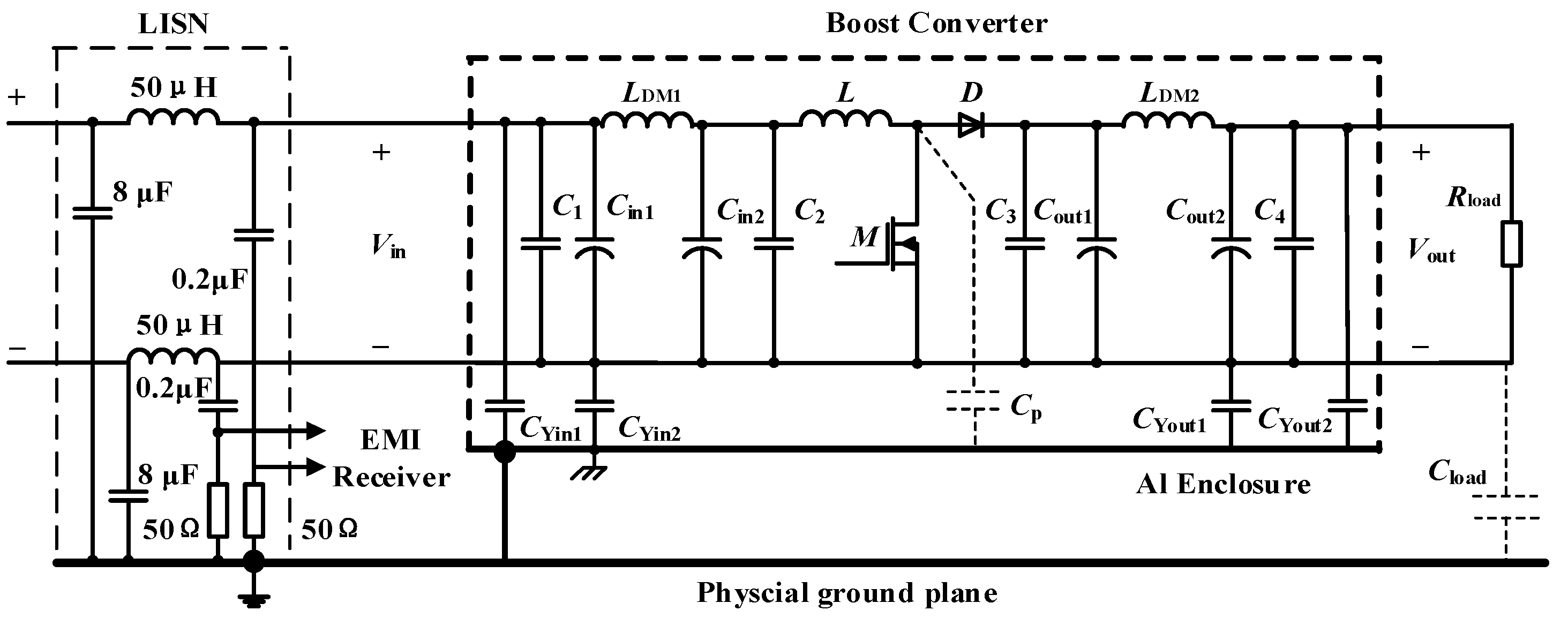
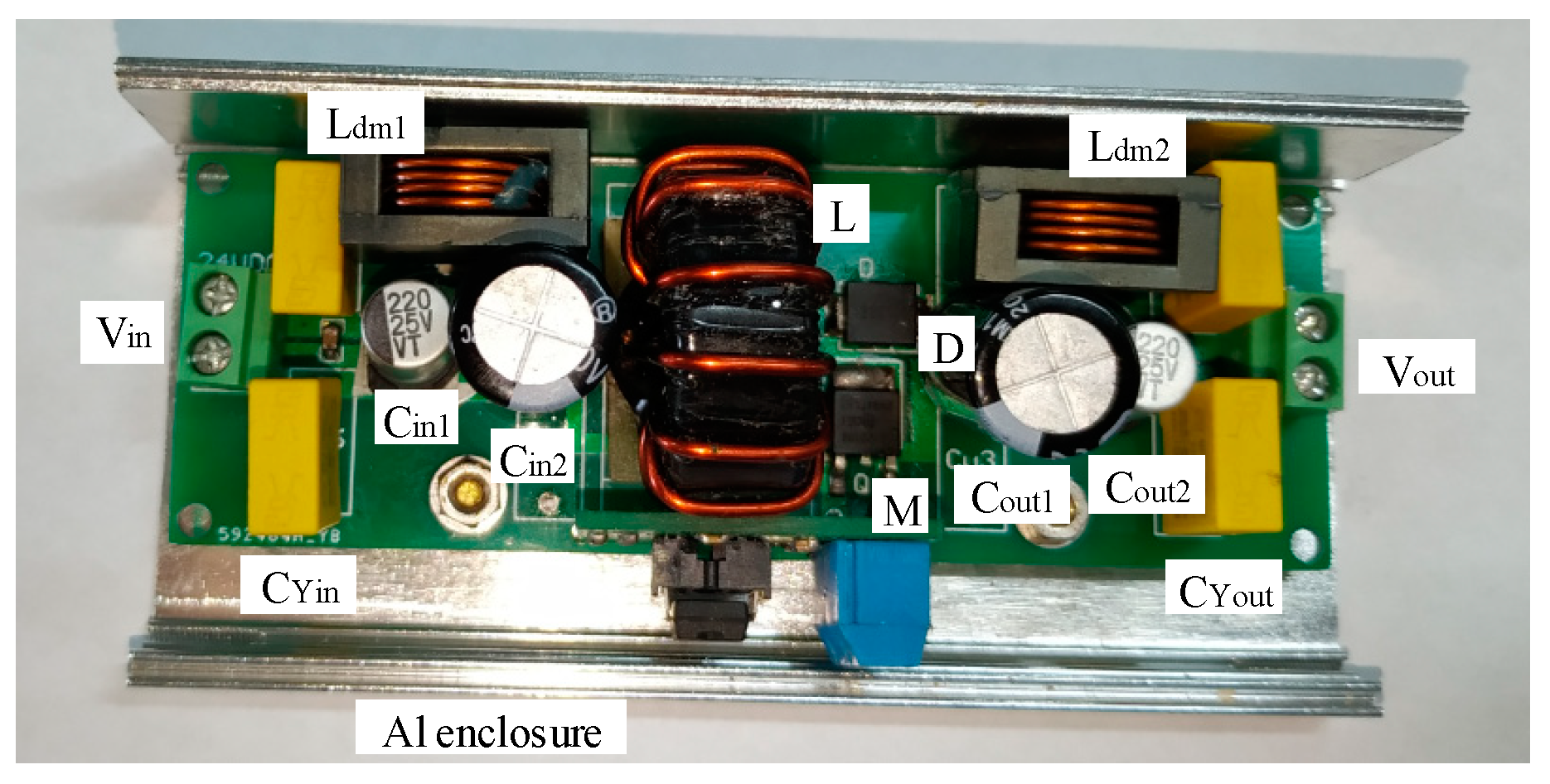
2.1. Boost Converter and Its Conducted Emission Test Layout

The studied boost converter is a common type DC/DC power supply in industrial and civil applications. Naturally, a boost converter can produce strong DM and CM conducted emission for its high dv/dt and di/dt switching operations, and this electromagnetic emission can usually be suppressed by an EMI filter composed of CM choke, CX capacitors and CY capacitors etc. However, the CM choke is not easy to manufacture because of its thick wire diameter in high current application fields, such as 12 V automobile low voltage power systems and 48 V telecommunication power system. Furthermore, its larger volume can reduce the power density of the converter as well. In order to overcome the above shortcomings, some boost products with low input voltage abandon CM choke, but only use CY capacitors to suppress CM conducted emissions. Although this CM filtering design has less insertion loss performance, it still has advantages in cost and volume, especially in large current and low voltage fields.
Figure 1 shows the main circuit topology of the studied low input voltage boost converter and its conducted emission test principle. This boost converter adopts the traditional LDM + CX DM filter and the single-stage CY CM filter at both the input and output ports as mentioned above. The whole boost converter is installed in an aluminum metal enclosure, which is directly connected with the physical ground plane. The dotted capacitor Cp and Cload in the figure represent the parasitic capacitor of the high dv/dt conductor of the main circuit to the metal enclosure and the parasitic capacitor of the Rload resistor to the ground, respectively. A standard 50 μH line impedance stability network (LISN) is used to detect the conducted emission. The conducted emission picked up by the 50 Ω resistor is sent to an EMI receiver, Laplace SA1000. The top front photo of the boost converter is shown in Figure 2. The main parameters of this boost converter are listed below. Input voltage Vin is 24 V; output voltage Vout is 42 V; load is 20 Ω; switching frequency fs is 214 kHz; inductor L is 7.8 μH; DM inductor LDM1, LDM2 is 0.68 μH; Cin and Cout are 220 μF; CYin1–CYout2 is 220 nF; aluminum metal enclosure is 2 mm thick. The inductor L in the main circuit is a toroidal inductor as shown in the middle of Figure 2. The print circuit board (PCB) layout design of the main circuit is generally rectangular and symmetrical.

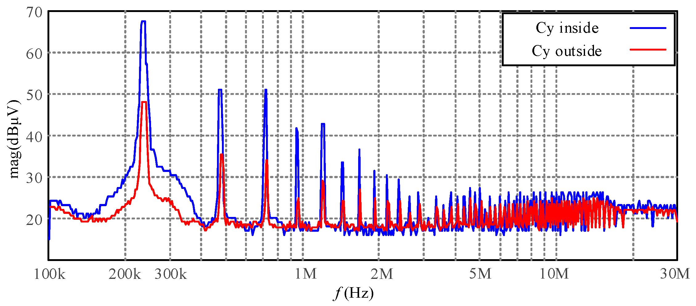
2.2. New Near-Field Coupling EMI Phenomenon and Its Diagnosis

An abnormal conducted emission phenomenon of the boost converter is observed during the conducted emission testing process. The actual measured CM conducted emission is much larger than the value predicted by the traditional EMI circuit model method [15], and it is even 20 dB higher at the switching frequency of 214 kHz. With reference to the research processes and results of the document [5,8,13], it can be inferred that there may be a near-field coupling effect in this boost converter. Since the near-field electromagnetic coupling theoretically exists between any two components, this will cause too many coupling parameters and greatly complicate the EMI circuit model. Therefore, it is necessary to determine the main coupling factors, properties, and coupling strength through reasonably designed experiments to grasp the essence of the EMI problem in engineering practice.
Two diagnosis experiments are carried out to determine whether there is an obvious near-field coupling effect in this boost converter. The detailed identification process is introduced below. First, the CY capacitors are moved from the inside of the enclosure to the outside, and the position movement schematic diagram is shown in Figure 3. Figure 4 shows the results of CM conducted emission measurement before and after moving the CY position. It can be found that the CM conducted emission has a significant change of more than 10 dB below 2 MHz. However, the measured DM conducted emission results remain unchanged at the same time. This result implies that there may be near–field coupling, because the near–field effect can be greatly affected by the component’s position and distance, while the results predicted by the traditional conducted emission EMI model without considering near–field coupling will not be affected by the CY position. Furthermore, the CY capacitors are placed in the metal enclosure and the toroidal inductor L is rotated by an angle, such as 45° as shown in Figure 3. Figure 5 shows the measured results of CM emission in this case. Similarly, it can be found that the CM conducted emission has a significant change of nearly 10 dB below 2 MHz. The DM conducted emission changes a little at the same time. Consequently, the experiment results confirm that there is a strong near-field coupling effect in this boost converter again, and it clearly shows that the toroidal inductor has an obvious influence, which is consistent with the research results on the stray magnetic field of a toroidal inductor in the paper [14,16] to a certain extent.
According to the previous experimental results, only the CM conducted emission changes greatly, so it can be inferred that the CM conducted emission path may be affected. As shown in Figure 1; Figure 2, the main CM paths are composed of the CYin, the metal enclosure, the CYout and the PCB trace conductors of boost. Hence, they can be judged as the interfered sensitive paths; in this boost converter, the possible stray magnetic field or electric field sources, i.e., high dv/dt or di/dt components, are only the inductor L, MOSFET’s drain conductor and high frequency alterative current (AC) loop. Because the AC PCB bus has been designed according to the minimum loop area rule, that is, the very small spacing parallel layout, it produces little magnetic field leakage and is not a key factor. Furthermore, the previous experiment result has shown that the influence of inductor L is great, so it can be judged as the stray near–field source. When the inductor L rotates at a small angle, its parasitic capacitance to the enclosure changes little, while the CM conducted emission changes more significantly. This means that the near–field source has obvious directivity, so it can be judged that the leakage magnetic field of the inductor is the main near-field coupling source. The MOSFET’s drain conductor is an electric field source, but it has no obvious directivity, so it is only a common source rather than the main near-field coupling source.

3. Common Mode Conducted Emission Theory Model Including Magnetic Coupling

In order to clarify the magnetic coupling effect of CM conducted emission found in the previous section, it is necessary to establish the mechanism circuit model of CM conducted emission with coupling parameters. This section first introduces the specific process of common mode magnetic coupling modeling of the converter, then introduces the comprehensive common mode conduction emission theory model including main circuit and magnetic coupling, and uses it to explain various experimental phenomena in the previous section.

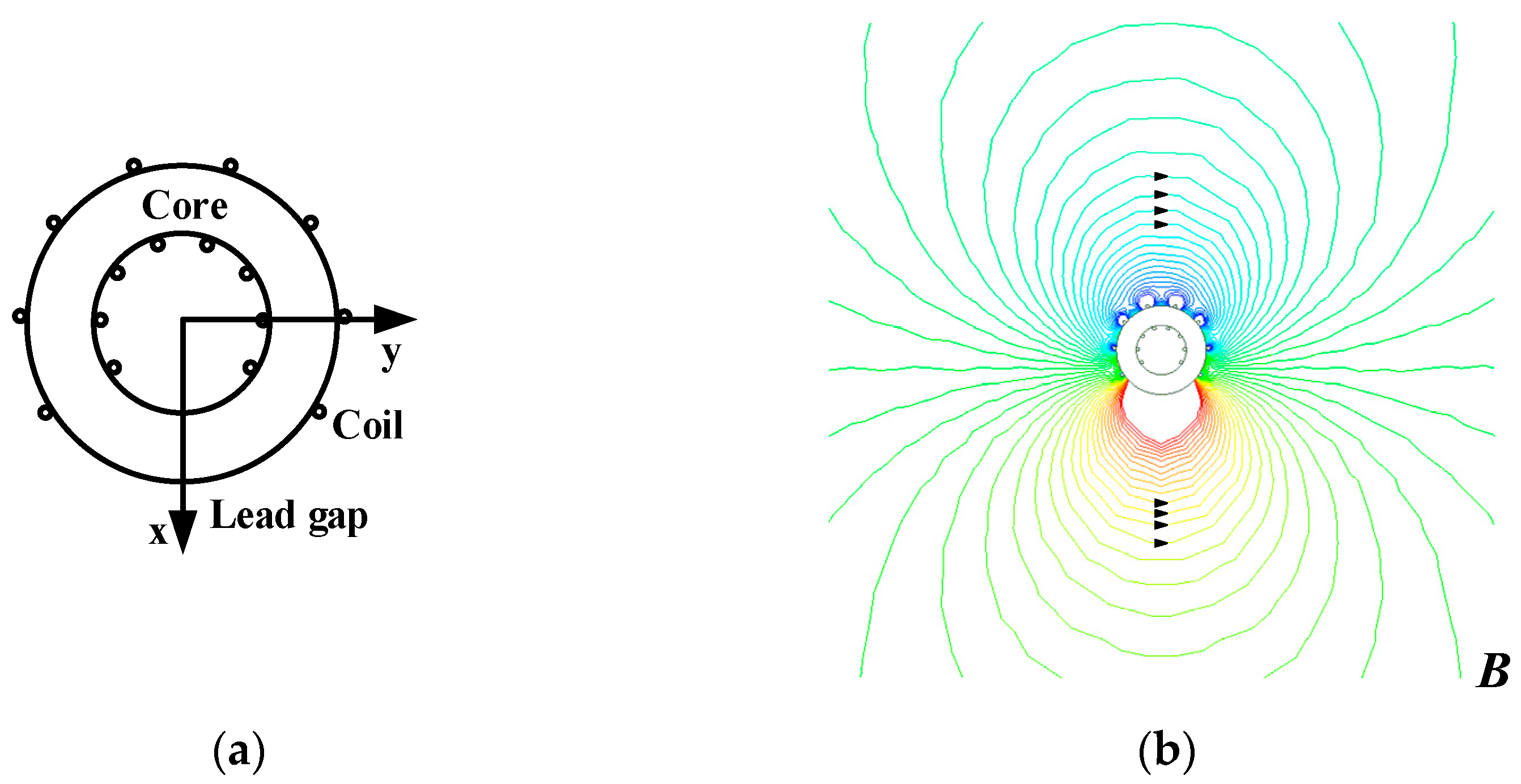
3.1. Stray Magnetic Field of the Toroidal Inductor

The leakage magnetic field of the toroidal inductor is firstly analyzed using electromagnetic simulation software in this section. The toroidal inductor L is a three-dimensional (3D) structure, so the magnetic field around it is naturally 3D distribution. For example [14,17], studied the stray magnetic field of a toroidal inductor using measurement or partial equivalent element circuit in detail. However, 3D electromagnetic modeling iscumbersome, and the comprehensive analysis and display of the 3D magnetic field is also a complicated task. In order to facilitate analysis and understanding, this paper adopts 2D electromagnetic modeling and simulation method, which can also reflect the key characteristics of the formation and distribution of the stray magnetic field.
The toroidal inductor of the boost converter uses a ferrite core, and its outer diameter, inner diameter and width of the core are 27 mm, 15 mm and 12 mm, respectively. The relative permeability of the core is 55. The wire diameter of the copper winding and turns are 1 mm and 8 turns, respectively. These turns are evenly distributed along the magnetic core except for the lead gap. Figure 6a shows the 2D structure of the toroidal inductor, and Figure 6b shows the 2D leakage flux around the core, which is simulated using finite element electromagnetic software, Ansoft Maxwell. This figure shows the distribution and direction of leakage flux in the air, in which the color from red to blue represents the gradual decrease of magnetic field intensity. It could be seen that the leakage flux lines are concentrated around the lead gap of the inductor, and the direction the leakage flux is mainly along the circumference direction of the core. In fact, further simulation can also show that the larger the lead gap is, the stronger the leakage magnetic field is.
As can be seen from Figure 2, the circumference of the toroidal inductor L is generally perpendicular to the conductors of the main circuit. This means that the leakage flux of the inductor just passes through the CM paths, which are composed of the CYin + the metal enclosure + the CYout + PCB conductors of the main circuit, thus forming mutual inductance couplings. These mutual inductance couplings between the toroidal inductor and the CM paths are schematically shown as Figure 7.

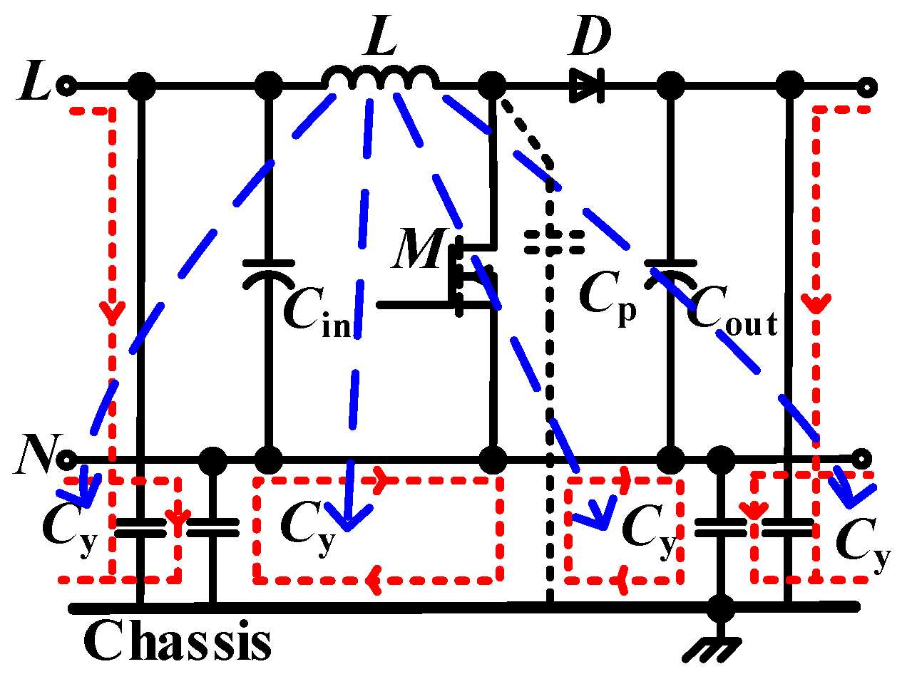
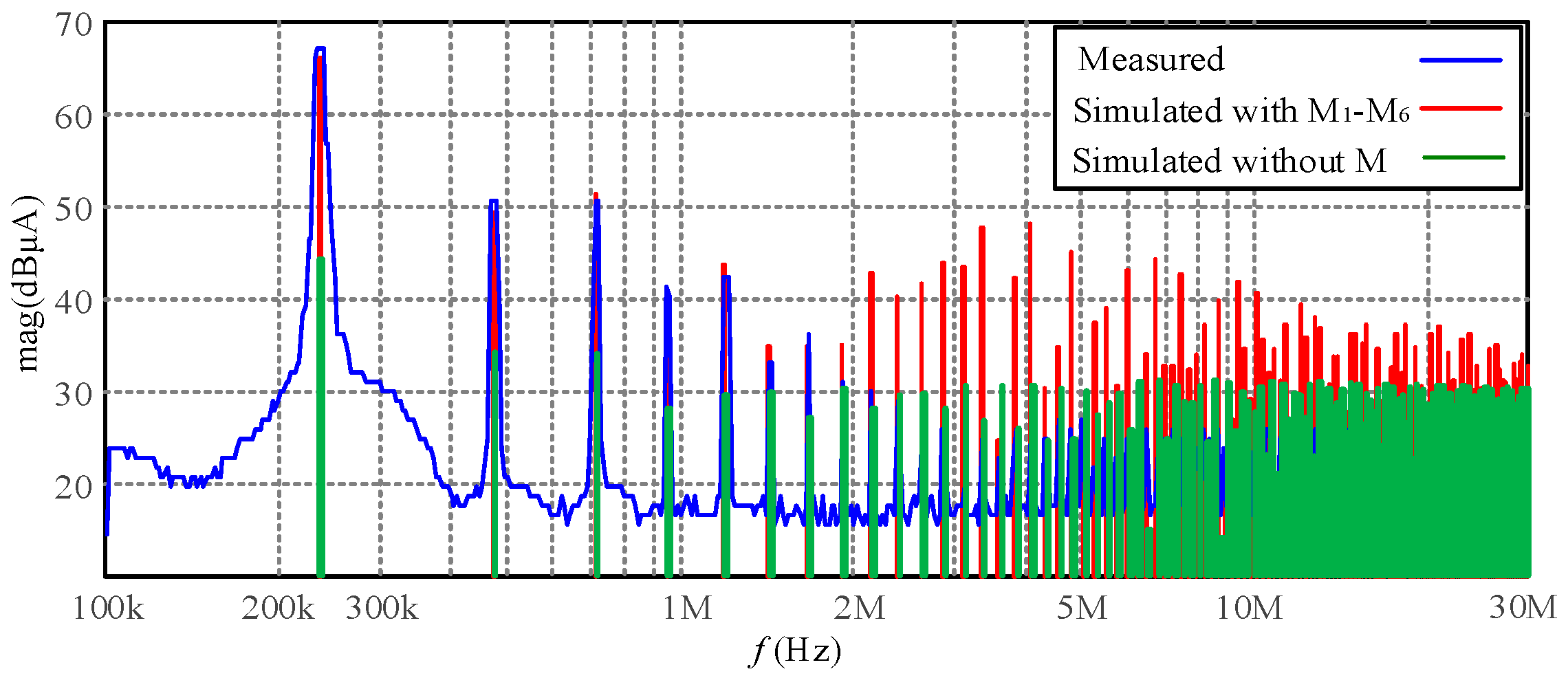
3.2. CM Conducted Emission Circuit Model including Magnetic Coupling Effect

In order to describe the magnetic coupling EMI phenomenon concisely, a CM conducted emission circuit model including magnetic coupling parameters is very necessary. However, the process of traditional conducted emission EMI modeling is cumbersome and complex [15]. In this paper, the following techniques are used to simplify the modeling while maintaining reliability. The Cin and Cout at input and output bus can be generally regarded as short circuit in the conducted emission frequency band due to their larger capacitance; the CYin1, CYin2 can be regarded as parallel connection, and CYout1, CYout2 are treated similarly; the inductance of the AL enclosure is very small for its enough thickness (2 mm) and its resistance is ignored to simplify EMI analysis. Furthermore, the MOSFET’s drain–source voltage Vds and its drain parasitic capacitance to metal chassis can be treated as a separated CM conducted emission branch, which is also the main cause of traditional CM noise. The magnetic couplings between the toroidal inductor and the CM paths can be represented as mutual inductance. These mutual inductances are treated as branch inductance, which is distributed on each conductor branch according to the partial inductance concept [11,16,17]. The toroidal inductor L can be treated as a separated sub-circuit because its current is the physical source of the stray magnetic field and can also be easily gotten by simulation or measurement. Finally, the refined CM conducted emission circuit model with magnetic coupling parameters of the boost converter can be obtained and shown as Figure 8.
As shown in Figure 8, Lp1–Lp4 represent the self-inductance of each section of PCB bus conductors. M1–M6 are the mutual inductance between the toroidal inductor and each branch of the CM paths. ESL, ESR are the parasitic inductance and resistance of CY capacitors respectively. Id is the current through the toroidal inductor L, and Vds is the drain–source voltage of MOSFET M. Cp is the parasitic capacitance between the dv/dt conductors and metal chassis. Cload is the parasitic capacitance between load and physical ground. The controlled voltage source U represents the reaction of mutual inductance to inductor L, which is naturally very small compared to Vds. The 25 Ω resistor on the left is the representation of the CM resistance of LISN. The parasitic impedance of the input/output cable of the converter is ignored for simplicity in this CM model, which brings little error in the low frequency band of conducted emission.
The specific values of the Vds, Id excitation sources and the parasitic parameters can be obtained by measurement or simulation methods. For example, mutual inductance M1–M6 can be extracted through the S parameter function method in finite element simulation software [13], Cp can be similarly extracted as well [15], and Vds and Id can be obtained through oscilloscope measurement or the SPICE circuit time-domain simulation method. Based on the circuit model in Figure 8, the CM conducted emission including the magnetic couplings can be obtained by frequency domain simulation. The simulated and measured CM conducted emission results are shown in Figure 9. The comparison clearly shows that the simulated results are consistent with the measured results from 150 kHz to 2 MHz, which verified the effectiveness of the CM model. Furthermore, if the magnetic couplings are not considered, i.e., all the mutual inductance, M1–M6 is set to 0, the CM emission of the CM EMI model can be simulated similarly and the result is shown using the green line in Figure 9. The simulated result without magnetic couplings is far less than the measured value below 2 MHz. These simulated results clearly show that mutual inductance plays a significant role in CM conducted emission, and the CM model simulations are consistent with the results of the experiment in Section 2.2.

4. Suppression Deigns of Magnetic Coupling

According to the analysis in previous sections, it will be an effective method to reduce the CM conducted emission by reducing magnetic couplings of the boost converter. This purpose can be achieved by improving the installation layout of the inductor or adjusting the structure of the inductor. This section introduces several suppression designs from the two aspects.

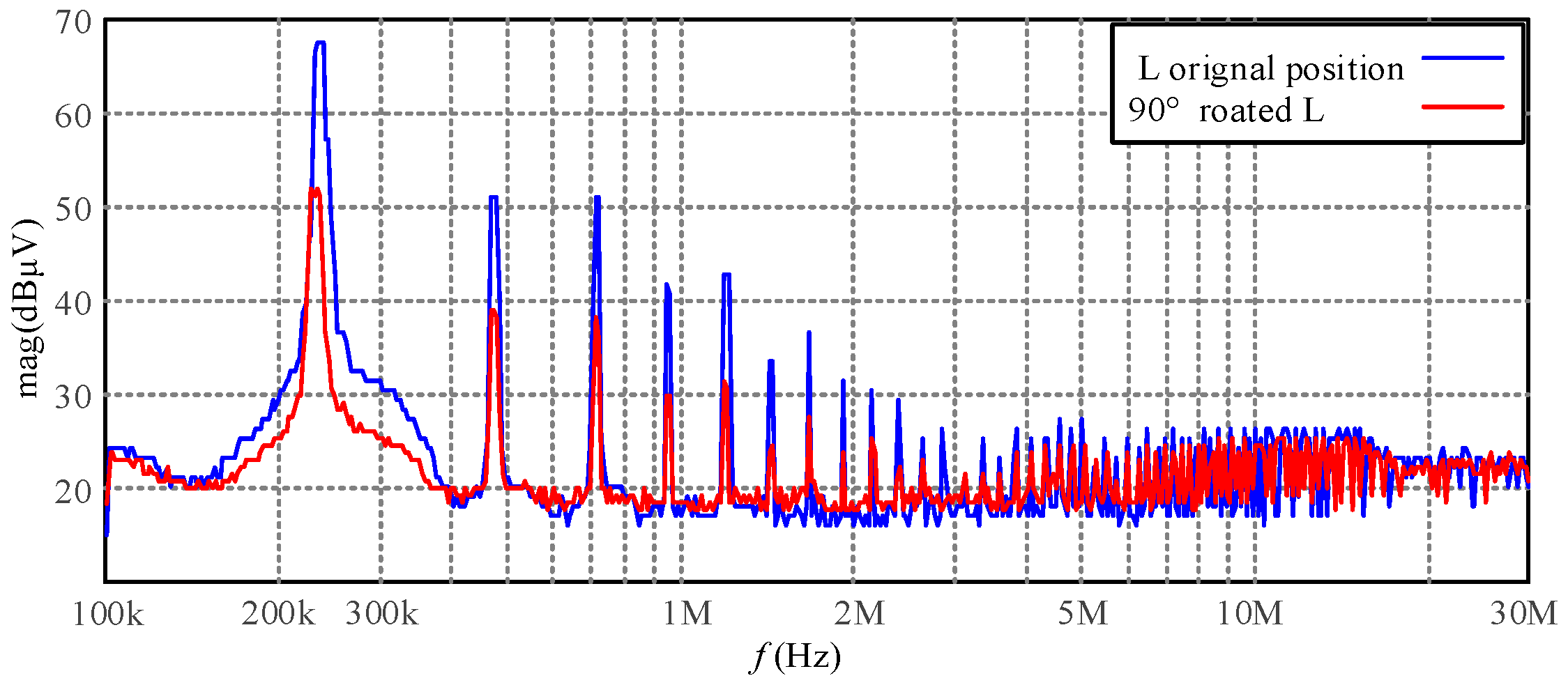
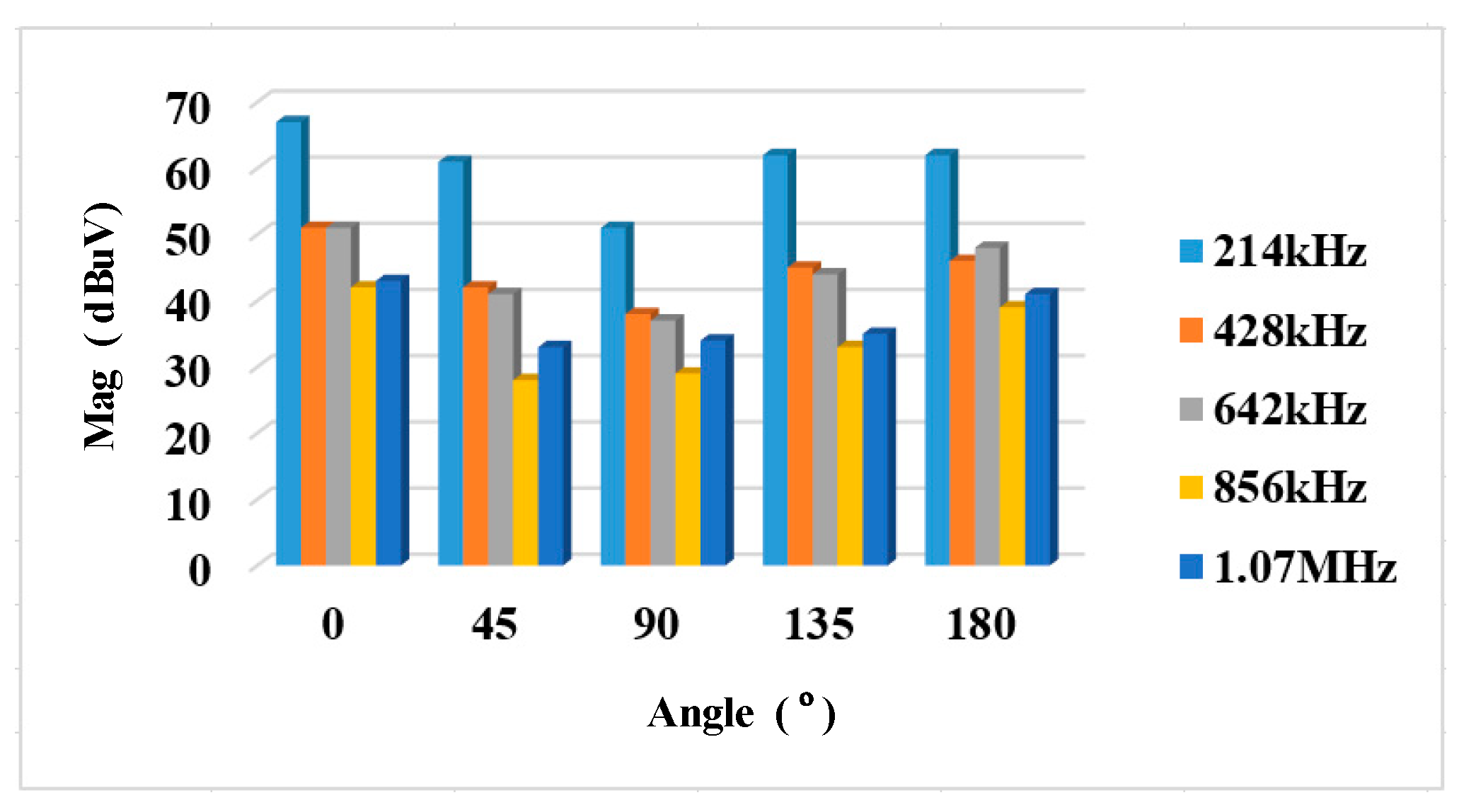
4.1. The Placement Angle Design of the Toroidal Inductor

Although the toroidal inductor is easy to produce a strong leakage magnetic field, the stray magnetic flux has obvious directionality and this feature can be used to decrease the magnetic coupling strength [5,14]. For this boost converter, the placement angle of the inductor L can be rearranged, and the flux link between the stray magnetic field and the CM paths can also change accordingly, thus the CM conducted emission will be changed as well. To verify the above analysis, the installation angle of the toroidal inductor is rotated counter–clockwise every 45° until it reaches 180°, as shown in Figure 3; the CM conducted emissions are also measured at these angles at the same time. Figure 10 shows the measured CM conducted emission histogram results before 1.2 MHz, it can be observed that the CM emission generally decrease 6–8 dB when the toroidal inductor rotates to 45° and 135°. Especially, the stray flux of the toroidal inductor has the least magnetic link with the CM paths when the toroidal inductor is rotated to 90°, then the CM conducted emission will be the least according to the CM EMI model of Figure 8. Results in Figure 10 also show that there is 10–18 dB decrease at 90°, which is consistent with the theoretical expectation. The experiment results verify the effectiveness of the placement design and can be used to optimize the component layout of a converter’s main circuit.

4.2. The Low Leakage Flux Designs of the Inductor

The leakage magnetic field of the toroidal inductor is mainly caused by the non–uniformity of its winding, which means that the control of leakage flux by winding precise arrangement is not an easy task, for this is difficult to achieve during production. If a different shaped magnetic core is adopted, for example, a ferrite core with an air gap in the center pillar, then the leakage flux around the inductor will be greatly reduced, thus the CM magnetic coupling in the boost converter will be greatly suppressed.
Since the EE and GU shaped magnetic core are commonly used in a power converter, an EE inductor and a GU inductor with the same inductance as the toroidal inductor are designed to test the previous analysis in this paper. Both inductors adopt the magnetic core design with an air gap in the center pillar. Figure 11 shows the 3D structure of EE shaped inductor and the simulation results of its surrounding leakage flux. It can be observed that the leakage flux is generally small for the side of the ferrite pillar with low reluctance. In addition, the direction of this leakage flux does not intersect the CM paths when the inductor is placed normally.
Figure 12a shows the EE shape inductor in the boost converter. Its CM conducted emission is measured and shown in Figure 12b. It is observed that the CM conducted emission drops obviously at the low frequency band. For example, there is about 14 dB improvement at the fundamental working frequency.
Similarly, the GU shaped inductor with an air gap in the center pillar has a low leakage flux distribution. Figure 13a shows the GU-shaped inductor in the boost converter. Its CM conducted emission curve is measured and shown in Figure 13b. It is observed that the CM emission also decreases obviously at the low frequency band. For example, there is a more than 20 dB improvement at fundamental working frequency.

5. Conclusions

This paper studies a new kind of magnetic coupling EMI phenomenon in a boost DC/DC converter. The abnormal larger CM conducted emission was found to be caused by the magnetic coupling effect. The coupling magnetic field source is the leakage flux of the toroidal inductor in the main circuit, which is linked to the CM paths of the boost converter directly; a concise CM conducted emission circuit model including magnetic coupling parameters is established. Simulated and measured results verify the effectiveness of the circuit model. This EMI circuit model also clearly shows that the magnetic field coupling directly causes the larger CM conducted emission in the 150 kHz–2 MHz frequency band. This paper also proposes several magnetic coupling suppression techniques, including the improved placement of key inductor and low leakage flux magnetic core designs, etc. The measured conducted emission results also prove the effectiveness of these new designs.
In general, the innovation points of this paper mainly include the following aspects: a new near field coupling EMI phenomenon is discovered and clarified for a boost power converter. Several reasonable and effective suppression design techniques are put forward. The research results of this paper also have good guiding significance for the EMC analysis and design of power converters in the field of electric vehicles and new energy power generation.

Author Contributions

Conceptualization, J.H. and Y.L.; methodology, Y.L.; software, L.C. and C.W.; validation, Y.L., C.W. and L.C.; formal analysis, Y.L. and J.H.; investigation, Y.L.; resources, J.H.; data curation, J.H. and L.C.; writing—original draft preparation, Y.L.; writing—review and editing, J.H., C.W. and L.C.; visualization, C.W.; supervision, J.H.; project administration, J.H.; funding acquisition, J.H. All authors have read and agreed to the published version of the manuscript.

Funding

This research was funded by the National Natural Science Foundation of China under Grant No.52077046 and Guangdong Natural Science Foundation under Grant 2020A1515010913.

Conflicts of Interest

The authors declare no conflict of interest.

References

  1. Jian, H.; Xiao, X.; Dongdong, C.; Guibin, L. Analysis and optimization of electromagnetic compatibility for electric vehicle. IEEE Electromagn. Compat. Mag. 2019, 8, 50–55. [Google Scholar]
  2. Robert, S.; Marcin, J.; Grzegorz, B.; Adam, K. AC/DC/DC Interfaces for V2G Applications—EMC Issues. IEEE Trans. Ind. Electron. 2013, 60, 930–935. [Google Scholar]
  3. Ruoxi, T.; Shangbing, T.; Cheng, Y.; Chenghao, D.; Anjian, Z. Research on electromagnetic-radiated emission of multi-in-one electric derive system. World Electr. Veh. J. 2021, 12, 127. [Google Scholar]
  4. Wang, S.; Lee, F.C.; Chen, D.Y.; Odendaal, W.G. Effects of parasitic parameters on EMI filter performance. IEEE Trans. Power Electron. 2004, 19, 869–877. [Google Scholar] [CrossRef]
  5. Junping, H.; Jianguo, J.; Wei, C. Identification and model of near field magnetic coupling in a PFC converter. In Proceedings of the 2005 IEEE 36th Power Electronics Specialists Conference, Dresden, Germany, 16 June 2005; pp. 323–327. [Google Scholar]
  6. Ashok, B. Wide-bandgap power devics: Adoption gathers moentum. IEEE Power Electron. Mag. 2018, 5, 22–27. [Google Scholar]
  7. Jianfei, C.; Minh-Khai, N.; Zhigang, Y.; Caisheng, W.; Le, G.; Gangyi, H. DC-DC Converters for Transportation Electrification: Topologies, Control, and Future Challenges. IEEE Electrif. Mag. 2021, 9, 10–22. [Google Scholar]
  8. Takahashi, K.; Murata, Y.; Tsubaki, Y.; Fujiwara, T.; Maniwa, H.; Uehara, N. Mechanism of near-field coupling between noise source and EMI filter in power electronic converter and its required shielding. IEEE Trans. Electromagn. Compat. 2018, 61, 1663–1672. [Google Scholar] [CrossRef]
  9. Hariya, A.; Koga, T.; Matsuura, K.; Yanagi, H.; Tomioka, S.; Ishizuka, Y.; Ninomiya, T. Circuit design techniques for reducing the effects of magnetic flux on GaN-HEMTs in 5-MHz 100-W high power-density LLC resonant DC–DC converters. IEEE Trans. Power Electron. 2016, 32, 5953–5963. [Google Scholar] [CrossRef]
  10. Wang, S.; Chen, R.; Van Wyk, J.D.; Lee, F.C.; Odendaal, W.G. Developing parasitic cancellation technologies to improve EMI filter performance for switching mode power supplies. IEEE Trans. Electromagn. Compat. 2005, 47, 921–929. [Google Scholar] [CrossRef]
  11. Chen, H.; Qian, Z.; Zeng, Z.; Wolf, C. Modeling of parasitic inductive couplings in a pi-shaped common mode EMI filter. IEEE Trans. Electromagn. Compat. 2008, 50, 71–79. [Google Scholar] [CrossRef]
  12. He, J.; Chen, W.; Jiang, J. Identification and improvement of stray coupling effect in an LCL common mode EMI filter. In Proceedings of the 2006 CES/IEEE 5th International Power Electronics and Motion Control Conference, Shanghai, China, 14–16 August 2006; pp. 1–5. [Google Scholar]
  13. Chen, H.; Qian, Z. Modeling and characterization of parasitic inductive coupling effects on differential-mode EMI performance of a boost converter. IEEE Trans. Electromagn. Compat. 2011, 53, 1072–1080. [Google Scholar] [CrossRef]
  14. Zhang, B.; Wang, S. Analysis and reduction of the near magnetic field emission from toroidal inductors. IEEE Trans. Power Electron. 2019, 35, 6251–6268. [Google Scholar] [CrossRef]
  15. Kharanaq, F.A.; Emadi, A.; Bilgin, B. Modeling of conducted emissions for EMI analysis of power converters: State-of-the-art review. IEEE Access 2020, 8, 189313–189325. [Google Scholar] [CrossRef]
  16. Kovačević, I.; Müsing, A.; Kolar, J.W. PEEC modelling of toroidal magnetic inductor in frequency domain. In Proceedings of the 2010 International Power Electronics Conference-ECCE ASIA, Sapporo, Japan, 21–24 June 2010; pp. 3158–3165. [Google Scholar]
  17. Kovačević, I.F.; Friedli, T.; Müsing, A.M.; Kolar, J.W. 3-D electromagnetic modeling of parasitics and mutual coupling in EMI filters. IEEE Trans. Power Electron. 2013, 29, 135–149. [Google Scholar] [CrossRef]
Figure 1. Boost converter and its conducted emission test layout.
Wevj 12 00225 g001
Figure 2. The front photo of the boost converter.
Wevj 12 00225 g002
Figure 3. Schematic diagram of changing CY and L position.
Wevj 12 00225 g003
Figure 4. CM emission curves when CY at inside/outside.
Wevj 12 00225 g004
Figure 5. CM emission curves when L is rotated or not.
Wevj 12 00225 g005
Figure 6. Toroidal inductor (a) 2D inductor structure; (b) 2D leakage flux distribution.
Wevj 12 00225 g006
Figure 7. Magnetic couplings among the toroidal inductor and CM paths.
Wevj 12 00225 g007
Figure 8. Basic CM conducted emission circuit model including magnetic coupling.
Wevj 12 00225 g008
Figure 9. Simulated and measured CM conducted emission.
Wevj 12 00225 g009
Figure 10. Measured CM conducted emission at different inductor placement angles.
Wevj 12 00225 g010
Figure 11. EE shaped inductor (a) 3D inductor structure; (b) 2D leakage flux distribution.
Wevj 12 00225 g011
Figure 12. EE shaped inductor and CM conducted emission (a) boost using EE shaped inductor; (b) CM conducted emission with different inductors.
Wevj 12 00225 g012
Figure 13. GU shaped inductor and CM conducted emission (a) boost using GU shaped inductor; (b) CM conducted emission with different inductors.
Wevj 12 00225 g013
Publisher’s Note: MDPI stays neutral with regard to jurisdictional claims in published maps and institutional affiliations.

