Article

Experimental Verification of Fault Tolerant Operation Focusing on DC-Bus Battery Failure in Dual Inverter Motor Drive

by
Yoshiaki Oto
*,
Toshihiko Noguchi
and
Melinda Badriatul Fauziah
Department of Electrical and Electronics Engineering, Shizuoka University, Hamamatsu 432-8561, Japan
*
Author to whom correspondence should be addressed.
World Electr. Veh. J. 2019, 10(4), 65; https://doi.org/10.3390/wevj10040065
Submission received: 15 September 2019 / Revised: 11 October 2019 / Accepted: 15 October 2019 / Published: 18 October 2019
(This article belongs to the Special Issue Power Electronics Subsystems)

Abstract

:
Recently, a dual inverter motor drive feeding an open-end winding permanent magnet (PM) motor has been studied, aiming for the improvement of total efficiency and a fault tolerant function of hybrid and electric vehicles. The authors have studied the fault tolerant operation of the DC-bus battery, where the failed inverter is operated only with a capacitor across the DC-bus and a space vector modulation (SVM) is employed to regulate the capacitor voltage. In our previous research, the SVM techniques for the fault tolerant operation in a low-modulation-index have been proposed. However, it was difficult to have fault tolerance in a high-modulation-index case. The voltage margin in the fault situation is limited because the failed inverter is operated with the capacitor. In this paper, the SVM technique to achieve the fault tolerant operation in the high-modulation-index state is investigated. The novel point of this paper is that the proposed technique introduces a field-weakening control in order to reduce the command voltage vector within the controllable voltage region. The proposed technique was verified through experimental tests and its operational characteristics were compared with the normal operation, from the viewpoints of the total harmonic distortion (THD) and the efficiencies of the inverters and the motor.

1. Introduction

Recently, a dual inverter motor drive feeding an open-end winding PM motor has been focused on, aiming for improvement of a total efficiency and a fault tolerant function of hybrid and electric vehicles. The dual inverter motor drive is expected to improve the efficiency of the system, because it can generate multilevel voltage waveforms across the motor windings by adding the output voltages of the inverters [1,2,3,4,5,6]. In addition, the dual inverter motor drive, where a DC-bus battery of one of the inverters is replaced with a capacitor, has also been studied [7,8,9,10,11,12]. In particular, it has advantages in many of the modern current hybrid and electric vehicles, over the C-segment. Most of all, the hybrid vehicles such as the Prius, Lexus, Camry and so forth, of the Toyota Motor Corporation employ the circuit topology depicted in Figure 1, using the voltage-boost chopper. Therefore, it is difficult to improve the total efficiency due to the significant power loss of the voltage-boost chopper and it can no longer continue to drive the motor, if either the chopper or the inverter fails. On the other hand, as shown in Figure 2, the dual inverter motor drive does not require any voltage-boost converter to apply the high voltage to the motor by adding the output voltages of both inverters. In addition, in the dual inverter motor drive studied in this paper, the DC-bus batteries are isolated in order to secure a fault tolerant function.
So far, the fault tolerant operation with the dual inverter motor drive—which focuses on failures of the switching devices—have been studied [13,14,15]. However, the fault tolerant operation of the DC-bus battery has not been considered in detail [16,17]. Therefore, the authors have focused on a redundancy in the switching states of the dual inverter motor drive and have studied the fault tolerant operation of the DC-bus battery [18,19]. In the studied operation, the failed battery is isolated with a relay, after some failure it is detected through the battery management system. Then, the failure side inverter is operated only with a capacitor across the DC-bus, instead of the isolated battery. In this case, the capacitor voltage of the failure side inverter must be controlled at half of the battery voltage of the other inverter in the normal operation by charging and discharging the capacitor. The topology of the operation in the fault situation is the same as the dual inverter motor drive, where one of the DC-bus batteries is replaced with the capacitor. However, in the conventional techniques, the capacitor voltage is controlled constantly, while generating the multilevel voltage waveforms across the motor windings by the phase difference of the fundamental voltage components between the two inverters [7,8,9,10,11,12]. On the other hand, in our studied technique, a space vector modulation (SVM) is employed and the redundancy of the dual inverter motor drive is utilized. In particular, the capacitor voltage must be discharged down to half of the battery voltage of the other inverter in the fault situation, immediately after the battery failure is detected, because both inverters have been operated with the battery and the battery voltages have been same in the normal operation. We proposed the SVM techniques to switch over the system to the operation in the fault case smoothly at a low-modulation-index [20]. However, it was difficult to achieve the fault tolerant operation at a high-modulation-index, because the DC-bus voltage of the failure side inverter is reduced by half, in other words, the voltage margin of the fault tolerant operation is limited.
In this paper, the SVM technique for the fault tolerant operation at the high-modulation-index is newly proposed, which controls the voltage command within the limited voltage region by employing a field-weakening control technique. However, it has the problem that unexpected error voltage pulses are generated in the multilevel voltage waveforms during a dead time [21,22]. In this paper, it is confirmed through experimental tests that the proposed fault tolerant operations at the high-modulation-index can continue to drive the motor even though one of the inverter DC-bus batteries fails. In addition, the operation characteristics in the fault case are compared with the normal operation characteristics, applying some techniques to reduce the error voltage pulses.

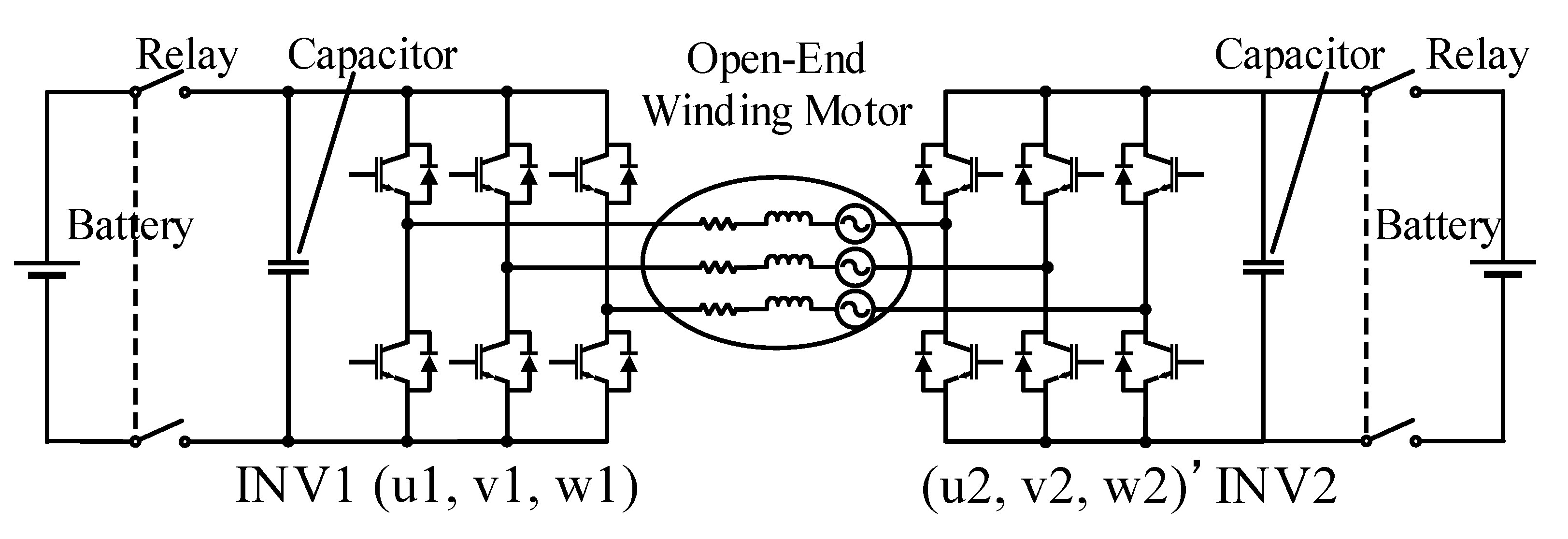
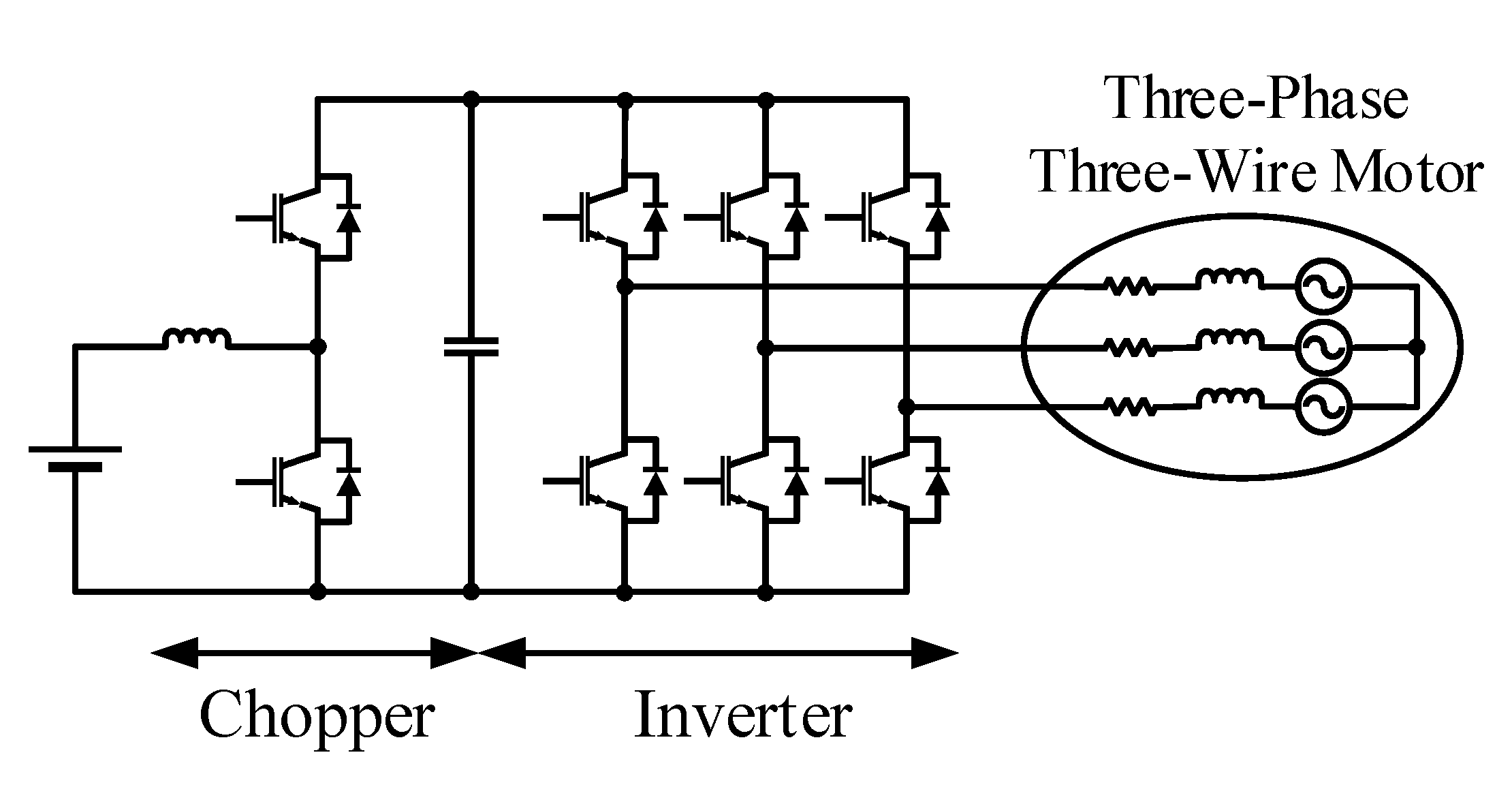
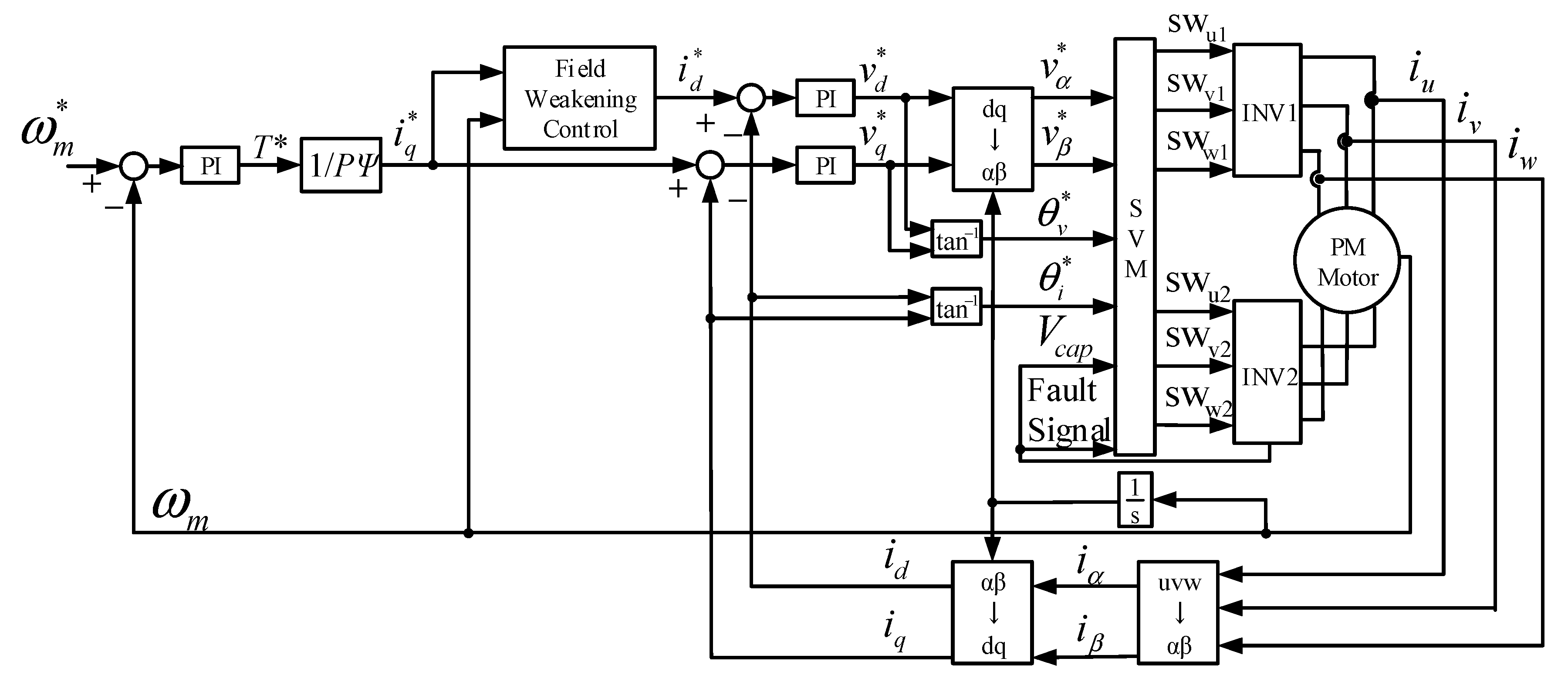
2. Dual Inverter Motor Drive

2.1. Circuit Configuration

The dual inverter motor drive feeds the open-end winding permanent magnet (PM) motor with two inverters, where the left inverter is INV1, the right one is INV2 and the switching states of the both inverters are described like (u1, v1, w1) (u2, v2, w2)’, as shown in Figure 2. In the switching state, “1” indicates that the upper arm is turned on and vice versa. Each leg is operated complementally. The DC-bus of each inverter has a battery, a capacitor and a relay to isolate the failed battery in case that some failure is detected in the battery. The dual inverter motor drive can generate the multilevel voltage waveforms across the motor windings by synthesizing the output voltage vectors of the two inverters. It is expected to improve the total harmonic distortion (THD) and the dv/dt of the output voltage waveforms, compared with the conventional single 2-level inverter motor drive. It is also expected to improve the total efficiency of the motor drive system, because it does not require any voltage-boost converter used in many of the hybrid and electric vehicles over the C-segment. Furthermore, the dual inverter motor drive has redundancy in the switching states, which means that there are several different switching states to generate a particular voltage vector. The redundancy makes it possible to achieve some fault tolerant operations of the dual inverter motor drive.

2.2. Fault Tolerant Operation of DC-Bus Battery

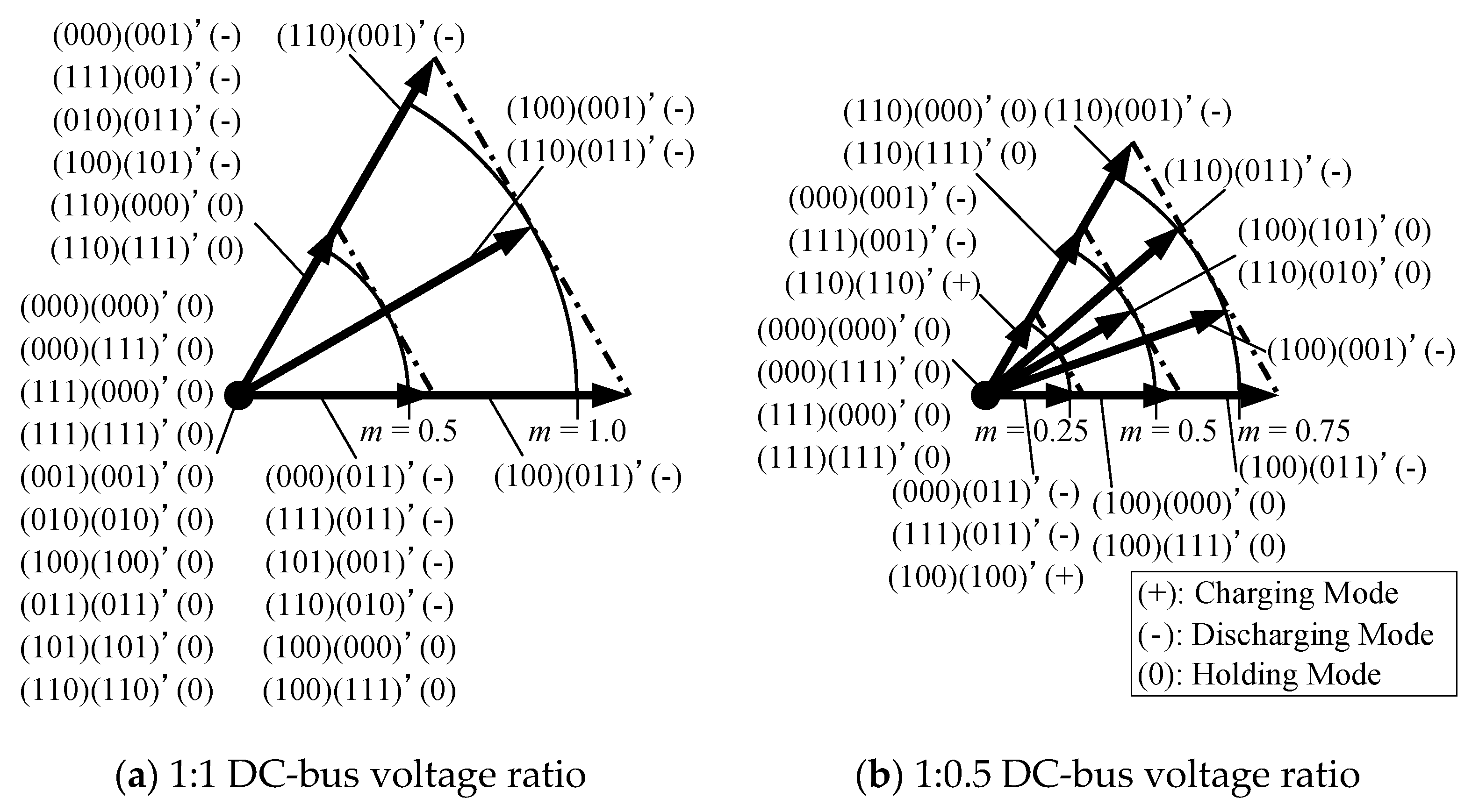
2.2.1. Operation Principle

In this paper, the fault tolerant operation of the DC-bus Battery is focused on, where it is assumed that the battery of INV2 fails. In the fault situation, the DC-bus battery of the INV2 is isolated with the relay, if some failure occurs in the battery. Then, the failed INV2 is operated only with the capacitor, instead of the isolated battery. In this case, it is necessary to control the capacitor voltage constantly and to generate multilevel voltage waveforms across the motor windings at the same time. Figure 3 shows the output voltage vectors and the switching states of the dual inverter motor drive from 0 to 60 degrees, where the capacitor charging and the discharging modes are also described. As shown in Figure 3 and described in Reference [19], the 1:0.5 DC-bus voltage ratio is employed and the capacitor voltage of the INV2 is controlled at half of the battery voltage of the INV1 in the fault situation, because it cannot switch over the charging mode and discharging mode redundantly in the case of the 1:1 DC-bus voltage ratio. However, the longest voltage vectors which configure the most outer region do not have the redundancy, even if the 1:0.5 ratio is employed. Therefore, in the fault tolerant operation of the DC-bus battery, the longest voltage vectors cannot be used for the SVM, in other words, the operation voltage region of the fault condition of the DC-bus battery is limited within the modulation-index m = 0.5.

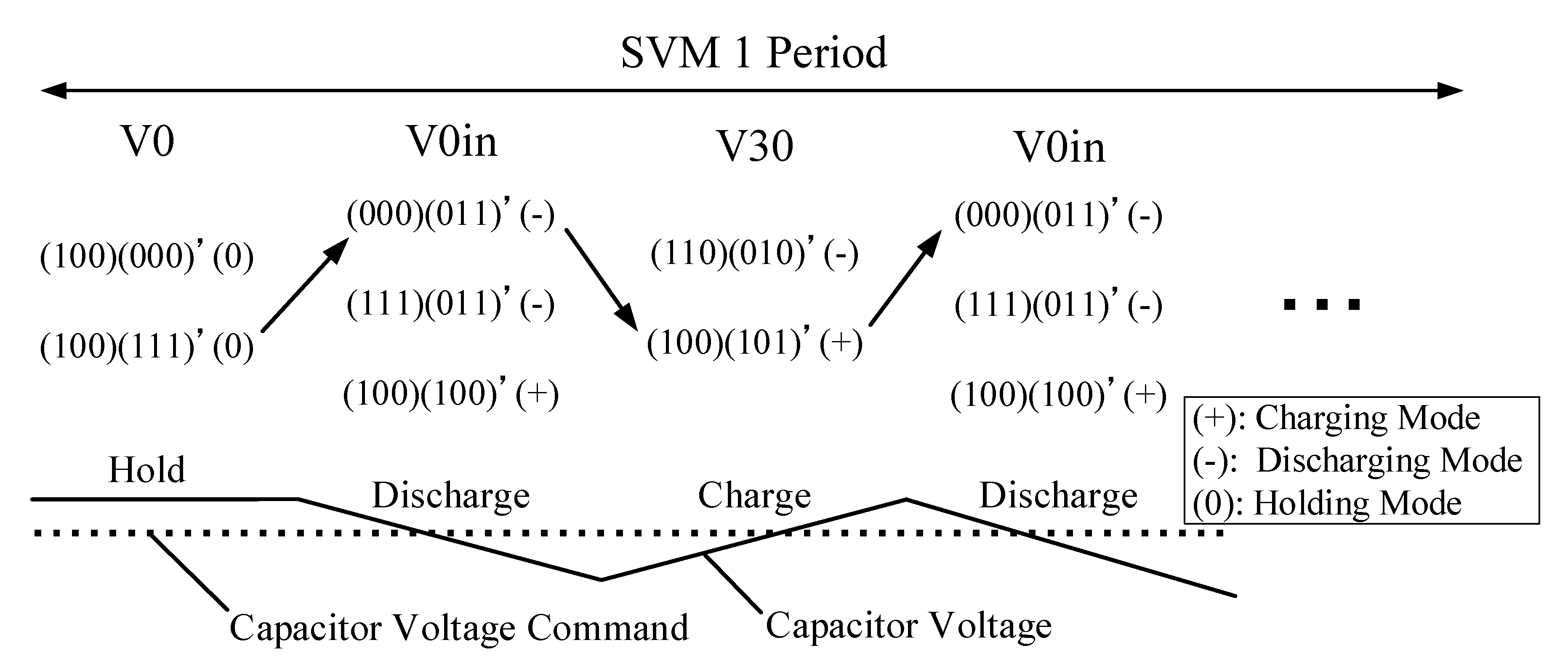
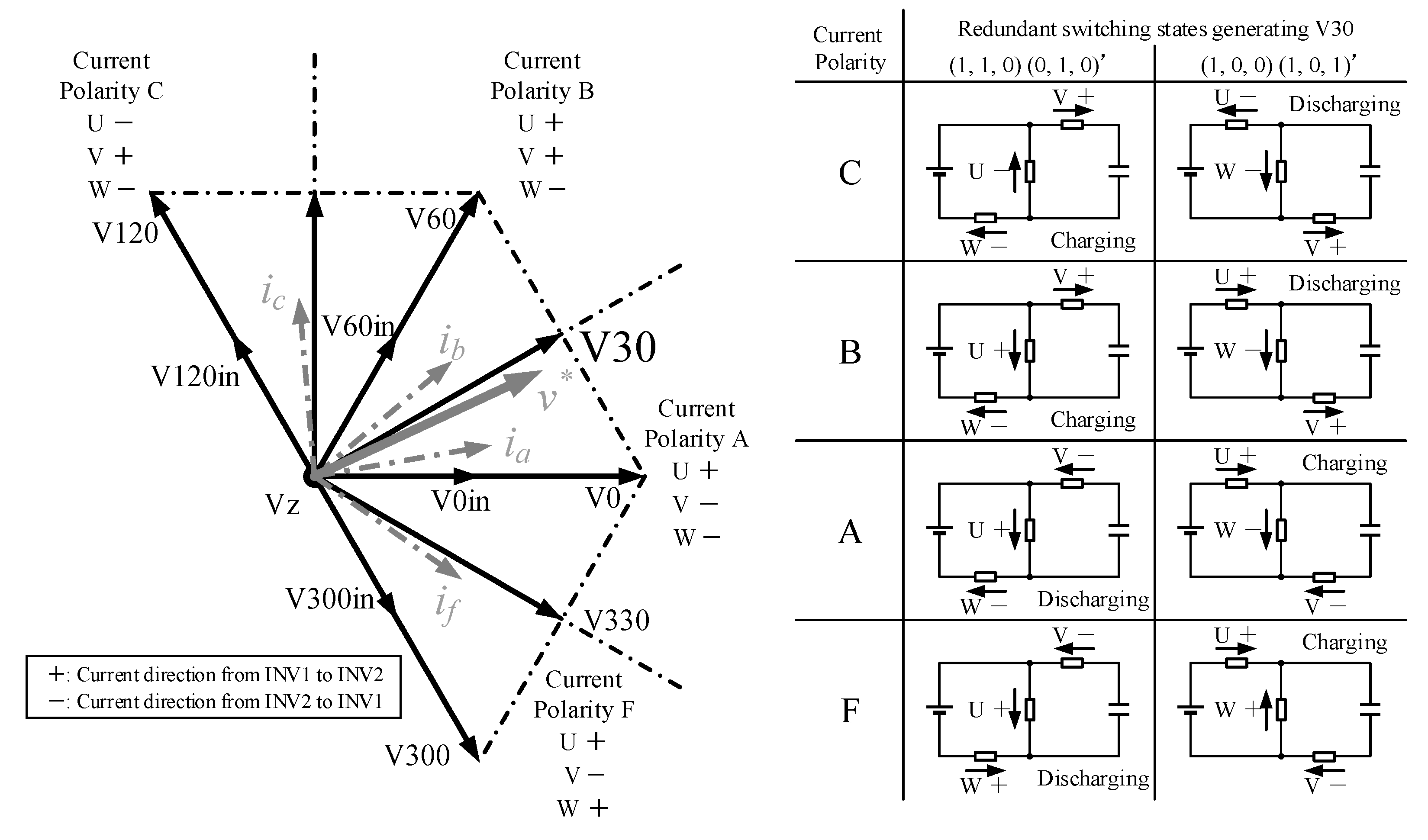
2.2.2. Capacitor Voltage Control with SVM

In this system, the SVM is employed to achieve both of the capacitor voltage control and the multilevel voltage waveform generation simultaneously. The switching sequence of the SVM can be configured flexibly. Therefore, when the command voltage vector is generated with the SVM, the SVM can control the capacitor voltage by selecting the most appropriate switching state which charges or discharges the capacitor appropriately in the redundant states. Figure 4 assumes that the dual inverter motor drive generates the command voltage vector v* in the hatched sector with the SVM, for example. The three voltage vectors V0, V0in and V30 surrounding the hatched sector are utilized to synthesize the v*. In the SVM, the time durations of each voltage vector utilized in the SVM are also calculated. The particular switching sequence case of the SVM is considered in Figure 5. As shown in Figure 5, when the voltage vector V0in is generated, the discharging mode is selected among the redundant states because the capacitor voltage is higher than its command value. Then, when the next voltage vector V30 is generated, the charging mode is selected because the capacitor voltage is lower than the command value. In this way, the capacitor voltage can be controlled at the command value, while generating the multilevel voltage waveforms to the motor simultaneously with the SVM.
However, the instantaneous motor power factor has an impact on the capacitor voltage control. Figure 6 shows the voltage vectors of the dual inverter motor drive from −60 to 120 degrees, which is the same case as Figure 4. In the figure, the current polarity is also described, which is defined by the directions of the motor line currents. The capacitor charging and discharging modes of each switching state can be determined by the current direction of the capacitor, that is, the current polarity. Since the motor is assumed to be an inductive load, the phase of the motor line current vector is delayed at most 90 degree with respect to the output voltage vector. On the other hand, in the case that maximum torque per ampere (MTPA) control or field-weakening control is employed, the phase of the current vector is advanced with respect to the output voltage vector. Therefore, the current polarity can be classified to F, A, B or C, in the case that the voltage vector v* is generated with the SVM. Figure 6 also shows the capacitor voltage control modes of the two redundant switching states generating the voltage vector V30. The switching state (1, 1, 0) (0, 1, 0)’ is the discharging mode in the current polarity A and F, for example. However, the identical switching state is the charging mode in the current polarity B and F. Therefore, the instantaneous motor power factor must be considered to select the capacitor charging or discharging mode among the redundant states in the capacitor voltage control as described in Reference [18].

2.3. Switching Over Techniques for Fault Tolerant Operation of DC-Bus Battery

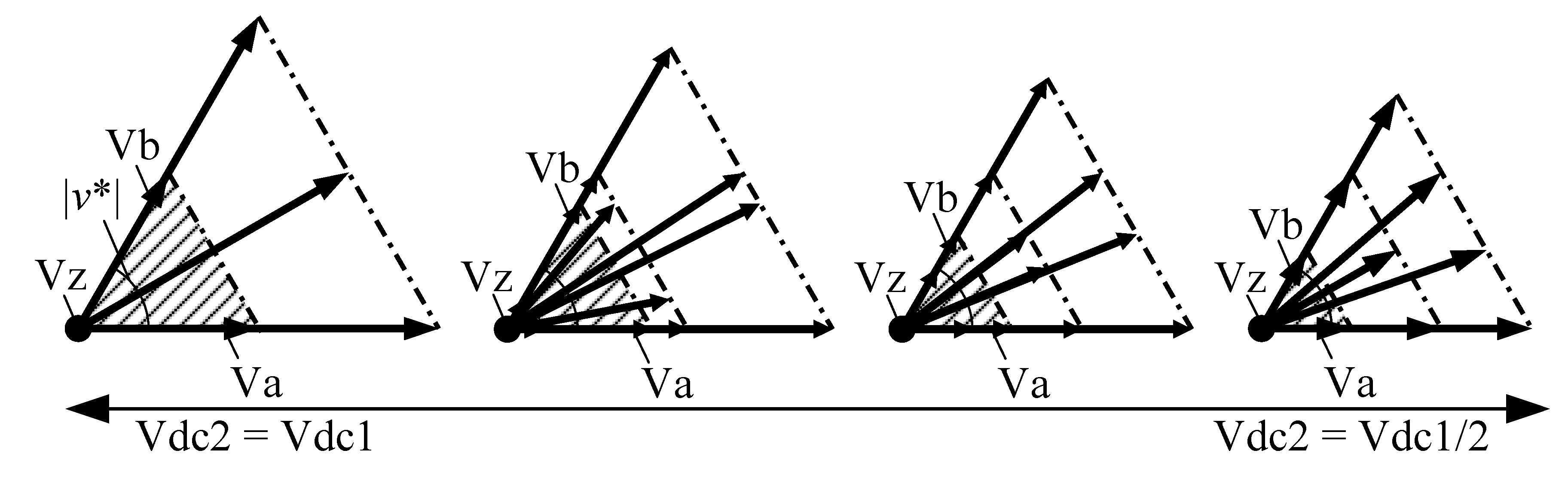
2.3.1. Switching Over Technique for Fault Tolerant Operation at Low-Modulation-Index

In this section, the failure of the DC-bus battery in the INV2 is assumed. In the normal operation of the dual inverter motor drive, both of the DC-bus battery voltages are same. However, once the failure occurs, the INV2 is operated with the capacitor and the capacitor voltage is controlled at half of the battery voltage of the INV1, in order to take advantage of the redundancy in the switching states [19]. Therefore, it is required to discharge the capacitor voltage of the INV2 down to the command value, immediately after the failed battery of the INV2 is isolated with the relay. However, in this time, a current flows into the battery of the INV1, which is in the normal condition, in order to discharge the capacitor voltage of the INV2. Besides, the amplitude and the phase of the voltage vectors generated by the dual inverter motor drive is changed because the capacitor voltage is discharged. Therefore, it is necessary to select the voltage vectors which synthesize the command voltage vector and to calculate the time durations of each voltage vector, considering the capacitor voltage.
Figure 7 and Figure 8 show the voltage vectors from 0 to 60 degrees in the case of the modulation-index 0 < m ≤ 0.25 and 0.25 < m ≤ 0.5, respectively. In both figures, the command voltage vector is generated in the hatched sector. The voltage vectors of the dual inverter motor drive are variable depending on the capacitor voltage, that is, the amplitude and the phase of each voltage vector are changed. Therefore, the SVM must be implemented, considering the capacitor voltage, as described in Reference [20]. In the case of the modulation-index 0 < m ≤ 0.25, the SVM is conducted with the three voltage vectors Vz, Va and Vb. On the other hand, in the case of the modulation-index 0.25 < m ≤ 0.5, the SVM is conducted with the three voltage vectors selected among the six voltage vectors Va, Va’, Vb, Vb’, Vc and Vc’. The switching over operation for the fault tolerant function of the DC-bus battery in the low-modulation-index m ≤ 0.5 can be achieved with the SVM by selecting the appropriate voltage vectors which discharge the capacitor voltage and calculating the time durations of each voltage vector, depending on the capacitor voltage.

2.3.2. Switching Over Technique for Fault Tolerant Operation Employing Field-Weakening Control at High-Modulation-Index

The voltage region for the fault tolerant operation is limited within the modulation-index m ≤ 0.5, because the voltage vectors that configure the most outer region have no redundancy as described in Section 2.2.1. In other words, it is difficult to switch over the dual inverter motor drive to the fault situation at the high-modulation-index m > 0.5, while providing the constant output power to the motor. Therefore, in this paper, the SVM technique employing the field weakening control for the fault tolerant operation in the high-modulation-index is newly proposed. In the proposed technique, the amplitude of the command voltage vector is reduced within the controllable voltage region of the fault tolerant operation by weakening magnetic flux of the PM motor with the d-axis current. The d-axis current command i d * is determined by the Equation (2), which is calculated from the general voltage equation of the motor (1). In the equations, | v f w * | indicates the amplitude of the voltage vector command with the field-weakening, v d and v q indicate the d-axis and the q-axis voltages, i q indicates the q-axis current, L d and L q indicate the d-axis and the q-axis inductances, R , ω and Ψ indicate the phase resistance, the rotating speed and the number of a flux linkage of the motor, respectively. The | v f w * | is determined to be controllable by the fault tolerant operation, that is, the modulation-index m < 0.5. However, in the Equation (2), the nominal values of the L d and the L q are used to calculate the i d * and the calculation of the i d * is implemented with an open loop. In this case, the calculation of the i d * cannot be implemented accurately, because the L d and the L q can be fluctuated due to a magnetic saturation. Therefore, the accurate identification of the L d and the L q is necessary to calculate i d * in the proposed fault tolerant operation in the high-modulation-index case. In Reference [23], an on-line identification technique of the L d and the L q is presented. The accurate calculation of the i d * can be achieved with the identification technique but the practical application of the identification technique is one of our future works.
[ v d v q ] = [ R + p L d ω L q ω L d R + p L q ] [ i d i q ] + [ 0 ω Ψ ]
i d * = Ψ L d ± ( | v f w * | ω L d ) 2 ( L q L d ) 2 i q 2
Then, after the voltage vector command is controlled to be within the modulation-index m < 0.5 with the proposed SVM technique, the dual inverter motor drive in the fault situation is controlled depending on the SVM technique for the fault tolerant operation in the low-modulation-index. However, in the case that the negative d-axis current flows, the phase of the motor line current vector is advanced with respect to the command voltage vector. Therefore, the capacitor voltage control with the SVM must be conducted, considering the phase difference between the line current and the command voltage vectors as described in Section 2.2.2.

2.4. Impact of Dead Time in Dual Inverter Motor Drive

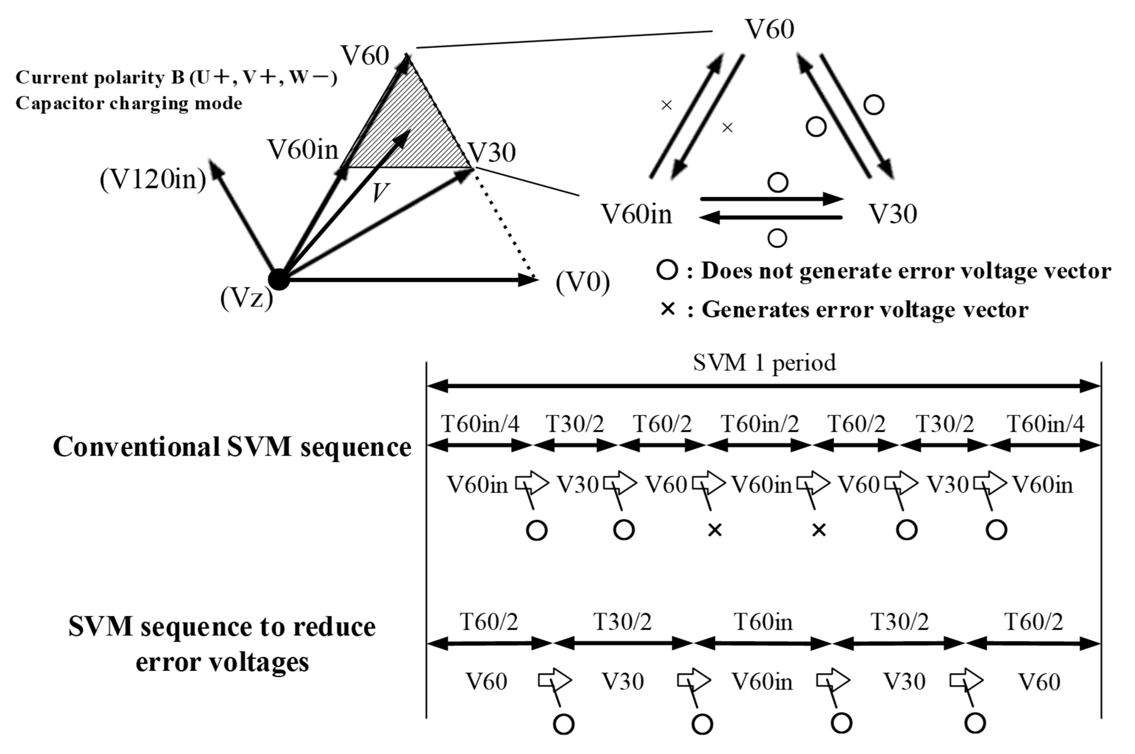
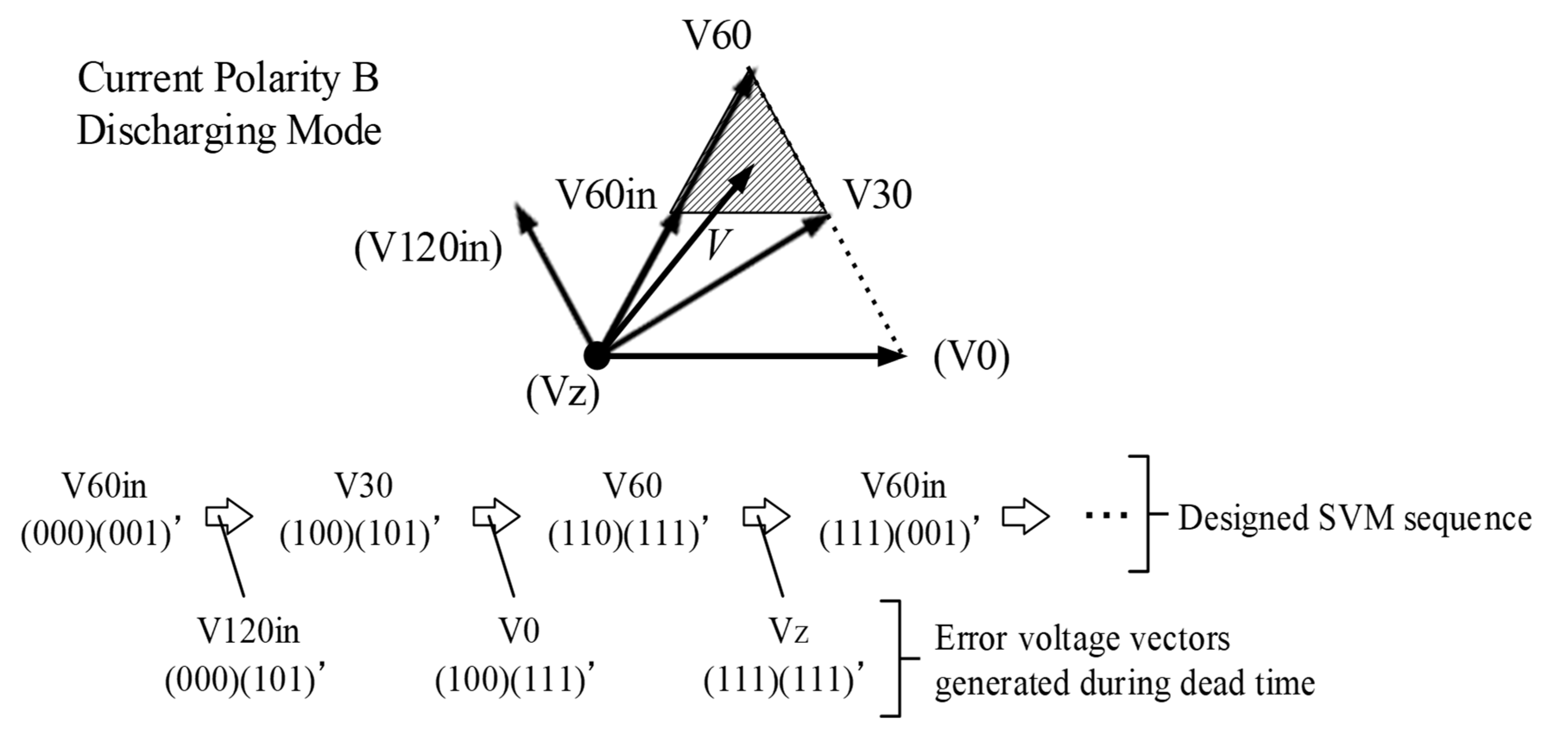
2.4.1. Error Voltage Vector During Dead Time

The SVM of the fault tolerant operation of the DC-bus battery in the dual inverter motor drive has particular switching transitions, which generates unexpected error voltage pulses in the multilevel voltage waveforms during a dead time. For example, synchronously turning off of upper arms in the same phase of both inverters is shown in Figure 9, where the devices in the same phase are switched over from the switching state A to the switching state B. In the designed SVM sequence, the switching state A must be changed to state B directly. However, unexpected error voltages can be generated during a dead time. The switching state during the dead time is determined by the motor line current direction, because the gate signal “0” are inputted to the switching devices of upper and lower arms of both inverters. Therefore, the switching devices are turned on with the diode during the dead time. In the switching state during the dead time of the synchronously turn off, as shown in Figure 9, the upper arm of the INV1 is turned off but the upper arm of the INV2 is turned on, which is an unexpected switching state during the dead time. The unexpected switching state causes error voltage pulses in the multilevel voltage waveforms as shown in Figure 10. In the case of generating the command voltage vector in the hatched sector, the three voltage vectors V30, V60 and V60in are utilized for the SVM and the switching sequence is configured as shown in Figure 10, for example. The designed SVM sequence is “V60in → V30 → V60 → V60in ∙∙∙”, however, the error voltage vectors such as V120in, V0 and Va are generated during the dead time due to the particular switching transitions.

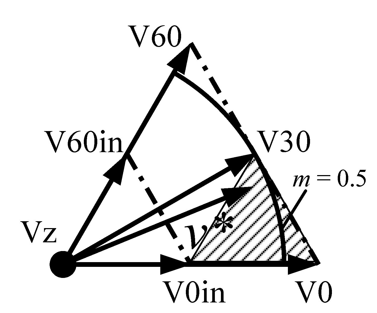
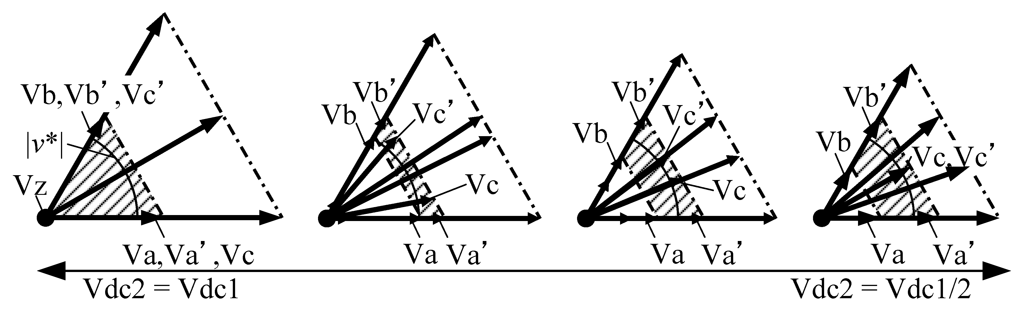
2.4.2. SVM Techniques to Reduce Error Voltages

The dead time scheme to avoid the error voltage vectors during the dead time is introduced in Reference [21]. In order to avoid the error voltage vectors, the dead time of each inverter is generated alternately as shown in Table 1, where the synchronously turn off is also assumed. The p1 and the p2 indicate the gate signals of the upper arms of the INV1 and the INV2 and the n1 and the n2 indicate the gate signals of the lower arms of the INV1 and the INV2, respectively. Moreover, the line current is assumed to flow from the INV1 to the INV2. In the state #2, a first dead time is generated to the inverter where the line current flows into, that is, the INV2. In the state, the upper arm of the INV1 keeps turn on and the upper arm of the INV2 is also turned on with the diode because the INV2 is during the first dead time. Then, at the end of the first dead time, a second dead time is generated to the other inverter, that is, the INV1. In state #3, the lower arm of the INV1 is turned on with the diode, because the INV1 is during the second dead time. On the other hand, the lower arm of the INV2 is also turned on, because the INV2 is after the first dead time. That is, the switching states in the same phase of the both inverters are changed from “1” to “0” directly. In this way, the dual inverter motor drive can be synchronously turned on or off without the error voltage vectors during the dead time.
The error voltage vectors are generated in other particular switching transitions, for example, the switching devices in the several phases of one inverter are synchronously turned on or off, even if the above dead time scheme is employed. Figure 11 shows the same situation as Figure 10. It also describes whether the error voltage vectors are generated during the dead time of every switching transition, where “○” means that the error voltages are not generated and the “×” means that the error voltages are generated even if the above dead time scheme is employed. As shown in Figure 11, the error voltage vector is sure to be generated in the switching transition between V60 and V60in.
A conventional SVM sequence, which is based on a general triangular-wave pulse width modulation (PWM), has seven switching states in one control period, that is, it cannot avoid the switching transition between V60 and V60in. On the other hand, it is possible to avoid the transition by designing the SVM sequence to have five states as described in Reference [22]. The block diagram and the algorithm of the SVM sequence which has five states are the same as the conventional sequence, for example, the capacitor charging or discharging mode of each switching state. Only the calculation method of the time durations of the voltage vectors used in the SVM is different from the conventional sequence. In this system, both the dead time scheme and the SVM sequence that has five states are employed, in order to reduce the error voltage vectors in the multilevel voltage waveforms.

3. Experimental Results and Discussion

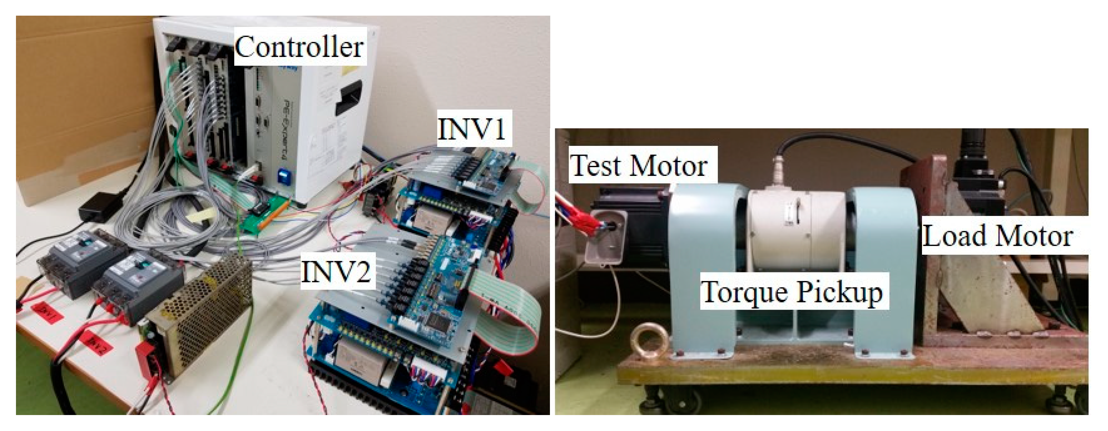
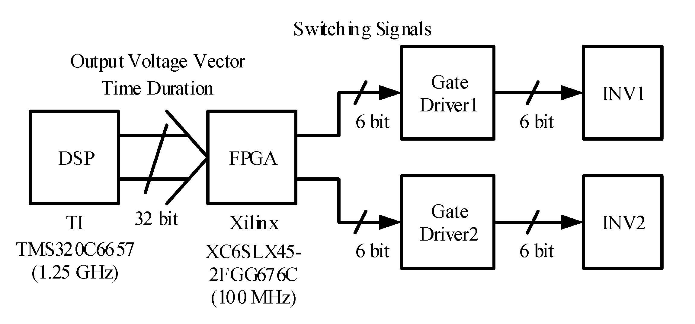
3.1. Experimental Setups

Experimental setups of the dual inverter motor drive are conducted as shown in Figure 12 and Table 2. The control brock diagram is also shown in Figure 13. The speed of the test motor is regulated at 1180 r/min with the load motor which is connected to the test motor. The test motor with the open-end windings is operated by the field-oriented control (vector control) algorithm with the two inverters. The rated output power of the test motor and the inverters are 1 kW and 5 kW, respectively. The INV2 has the relay to isolate the DC-bus battery across the DC-bus. In the normal operation, both inverters are operated with the battery across each DC-bus whose voltages are set at 100 V and the test motor is operated with MTPA control in the normal condition at the modulation-index m = 0.8. Then, after the fault signal is detected, the system is switched over to the fault situation where the INV2 is operated only with the capacitor. In this time, the capacitor voltage of the INV2 is discharged down to 50 V with the SVM and the test motor is operated by field-weakening control utilizing the negative d-axis current in order to reduce the amplitude of the command voltage vector within the controllable voltage region of the modulation-index m < 0.5. On the other hand, the q-axis current command and the motor rotating speed are constant between the normal operation and the fault tolerant operation; in other words, the output power of the dual inverter motor drive is constant.
Figure 14 shows a configuration of the controller. The controller has a digital signal processor (DSP: TMS320C6657) and a field-programmable gate array (FPGA: XS6SLX45-2FGG676C). The SVM algorithm is implemented in the DSP, where the voltage vectors are selected to synthesize the command voltage vector and the time durations of each voltage vectors are calculated. In this SVM algorithm, the three voltage vectors which are nearest the command voltage vector are selected according to a map created beforehand. Then, the appropriate switching states generating each voltage vector are selected among the redundant states to reduce the number of the switching transitions and to avoid the unexpected error voltage. In particular, the calculation of the time durations is conducted depending on the capacitor voltage in the fault situation. However, the SVM is required to switch over the switching devices of the inverters with a high-time-resolution. Therefore, the FPGA, which can generate the gate signals to the gate drivers of both inverters with the time-resolution of 100 MHz according to the calculation results of the DSP, is employed. In addition, the compensation technique to reduce the error voltage vectors during the dead time is also implemented in the FPGA.

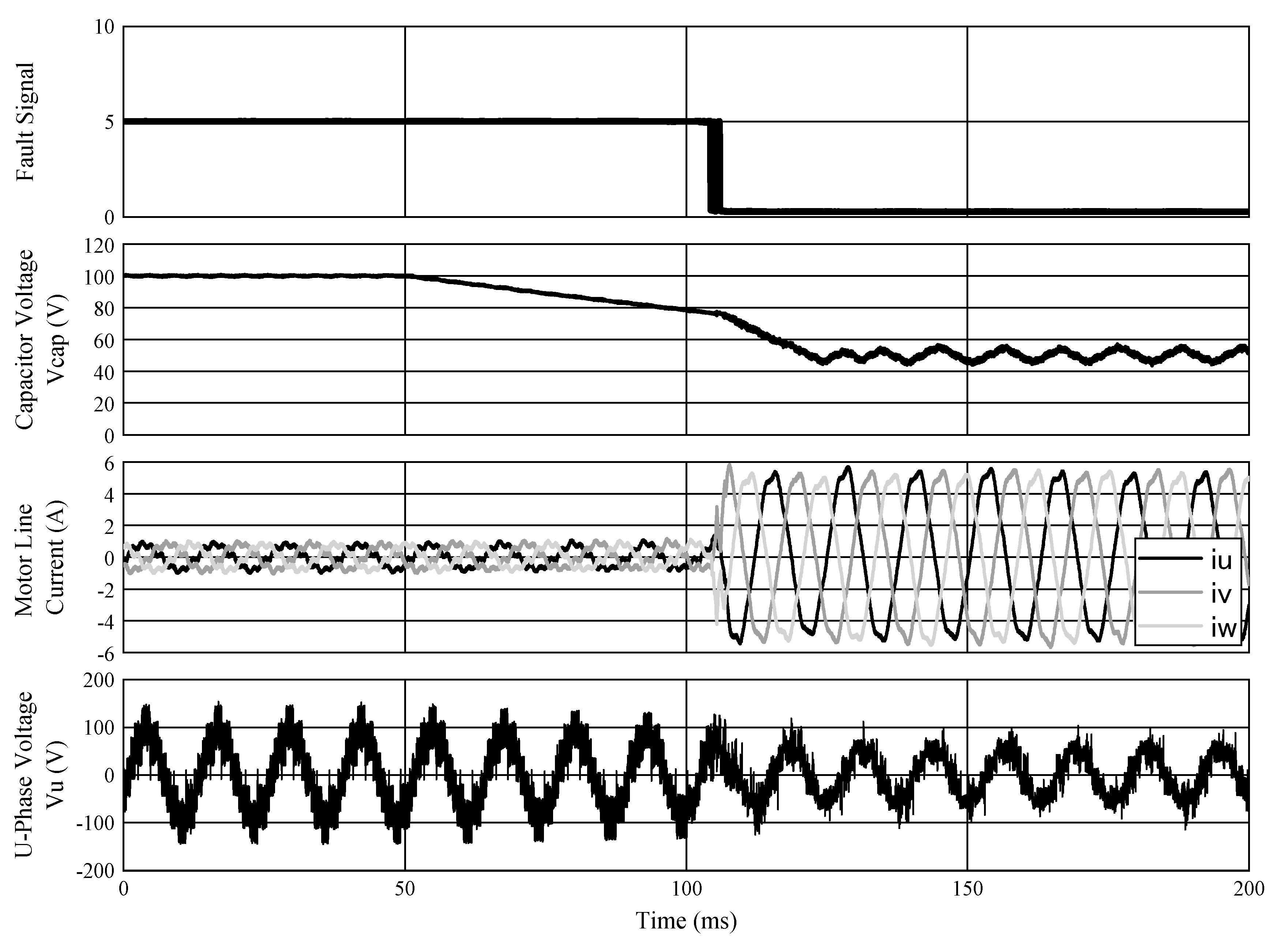
3.2. Experimental Results and Discussions

The experimental results are shown in Figure 15 and Table 3. In Figure 15, the fault signal of the DC-bus battery of the INV2, the capacitor voltage of the INV2, the three-phase currents of the motor, the voltage between the U-phase terminals of the INV1 and the INV2 are depicted. In the normal situation, the fault signal is 5 V, the capacitor voltage of the INV2 keeps at 100 V, the three-phase motor currents are balanced with the effective value irms = 0.59 A and the 9-level voltage waveform is generated across the U-phase winding of the motor with the measured THD 13.7%. Then, after the fault signal is detected, the system is switched over to the fault situation smoothly with the proposed SVM techniques in the high-modulation-index case. On the other hand, the fault tolerant operation of the DC-bus battery in the case of the low-modulation-index was also verified by the authors with several experimental test conditions, which was published in Reference [20]. However, the capacitor voltage starts to decrease before the SVM is switched over to the fault situation. In the experimental setup, in order to detect the fault signal of the DC-bus battery in the INV2, an analog circuit is connected across the relay to isolate the failed DC-bus battery, which is configured with Schmitt-triggers and RC-filters. Therefore, it takes time to output the fault signal to the controller. The dual inverter motor drive is operated with the SVM for the normal operation, until the fault signal is given to controller. As a result, the capacitor voltage cannot be controlled and is reduced before the operation is switched over to the fault situation. In fact, the time to detect the fault signal is reduced by using a voltage sensor in a battery management system of the Li-ion battery across the inverter DC-bus.
In the fault situation of the DC-bus battery in the INV2—as shown in Figure 15—the capacitor voltage of the INV2 is regulated at 50 ± 5 V by charging and discharging the capacitor with the SVM, the three-phase motor currents are balanced with the effective value irms = 3.74 A and the 9-level voltage waveform is generated across the U-phase winding of the motor with the measured THD 13.0%. The output voltage waveform in the fault situation still has error voltage pulses but achieves the approximately same THD as the normal operation waveform by employing the SVM techniques to reduce the error voltages during the dead time. The error voltage pulses caused by the synchronous switching transition in the same phases of both inverters can be improved, if the corresponding semiconductor devices carry out perfectly simultaneous turning on or off. However, the perfect simultaneous switching is actually difficult because the phase current flows through the diode in one side device and the insulated gate bipolar transistor (IGBT) in the other side device. Therefore, the switching transition time is different between the two inverters. Besides, the error voltage pulses can be generated at the point of the transitions between the capacitor charging and the discharging modes and between the operating regions of the SVM, for example. Therefore, it is difficult to eliminate the voltage ripple completely.
The efficiency measured results of the INV1 and the motor are deteriorated by 7.9% and 90.2%, respectively. The reason why the measured efficiency of the INV1 is deteriorated is that the switching loss and the conduction loss are increase due to the d-axis current in the field-weakening control. Moreover, the reason why the measured motor efficiency is deteriorated is that the d-axis current does not contribute to the motor torque and the motor rotating speed, that is, the output power of the motor. However, it is difficult to measure the efficiency of the INV2 in the fault situation, because the INV2 utilizes only a reactive power.

4. Conclusions

This paper describes the fault tolerant operation of the dual inverter motor drive focusing on the DC-bus battery failure with the SVM. The SVM technique for the fault tolerant operation in the high-modulation-index is proposed for the first time in this paper. The proposed technique was verified through experimental tests and the operation characteristics of the fault situation were assessed and compared with the normal operation from the viewpoints of the measured THD and the efficiencies of the inverter and the motor.

Author Contributions

Conceptualization, Y.O. and T.N.; methodology, Y.O., T.N. and M.B.F.; software, Y.O.; validation, Y.O., T.N. and M.B.F.; formal analysis, Y.O.; investigation, Y.O. and M.B.F.; data curation, Y.O.; writing—original draft preparation, Y.O.; writing—review and editing, Y.O. and T.N.; visualization, Y.O.; supervision, T.N.; project administration, T.N.; funding acquisition, T.N.

Funding

This work was supported by the New Energy and Industrial Technology Development Organization (NEDO), Grant-in-Aid for Scientific Research from the National Government and Ministry of Economy, Trade and Industry, Japan.

Conflicts of Interest

The authors declare no conflict of interest.

References

  1. Kiadehi, A.D.; Drissi, K.E.K.; Pasquier, C. Voltage THD Reduction for Dual-Inverter Fed Open-End Load with Isolated DC Sources. IEEE Trans. Ind. Electron. 2017, 64, 2102–2111. [Google Scholar] [CrossRef]
  2. Wu, D.; Wu, X.; Su, L.; Yuan, X.; Xu, J. A Dual Three-Level inverter -Based Open-End Winding Induction Motor Drive with Averaged Zero-Sequence Voltage Elimination and Neutral-Point Voltage Balance. IEEE Trans. Ind. Electron. 2016, 63, 4783–4795. [Google Scholar] [CrossRef]
  3. Somasekhar, V.T.; Srinivas, S.; Kumar, K.K. Effect of Zero-Vector Placement in a Dual -Inverter Fed Open-End Winding Induction-Motor Drive with a Decoupled Space-Vector PWM Strategy. IEEE Trans. Ind. Electron. 2008, 55, 2497–2505. [Google Scholar] [CrossRef]
  4. Umeshi, B.S.; Sivakumar, K. Dual-Inverter-Fed Pole-Phase Modulated Nine-Phase Induction Motor Drive with Improved Performance. IEEE Trans. Ind. Electron. 2016, 63, 5376–5383. [Google Scholar] [CrossRef]
  5. Somani, A.; Gupta, R.K.; Mohapatra, K.K.; Mohan, N. On the Causes of Circulating Currents in PWM Drives with Open-End Winding AC Machines. IEEE Trans. Ind. Electron. 2013, 60, 3670–3678. [Google Scholar] [CrossRef]
  6. Mitsudome, K.; Haga, H.; Kondo, S. Improvement of Output Voltage Waveform in Dual Inverter Having a Different DC Power Supply. In Proceedings of the IEEJ Technical Meeting on Semiconductor Power Converter and Motor Drive, Osaka, Japan, 23–24 January 2015; pp. 77–82. [Google Scholar]
  7. Ewanchuk, J.; Salmon, J.; Chapelsky, C. A Method for Supply Voltage Boosting in an Open-Ended Induction Machine Using a Dual Inverter System with a Floating Capacitor Bridge. IEEE Trans. Power Electron. 2013, 28, 1348–1357. [Google Scholar] [CrossRef]
  8. Machiya, H.; Haga, H.; Kondo, S. High Efficiency Drive Method of an Open-Winding Induction Machine Driven by Dual Inverter using Capacitor Across DC Bus. IEEJ Trans. Ind. Appl. 2015, 135, 10–18. [Google Scholar] [CrossRef]
  9. Corzine, K.A.; Wielevski, M.W.; Peng, F.Z.; Wang, J. Control of Cascaded Multi-Level Inverters. IEEE Trans. Power Electron. 2004, 19, 732–738. [Google Scholar] [CrossRef]
  10. Corzine, K.A.; Lu, S.; Fikse, T.H. Distributed Control of Hybrid Motor Drives. IEEE Trans. Power Electron. 2006, 21, 1374–1384. [Google Scholar] [CrossRef]
  11. Kim, J.; Jung, J.; Nam, K. Dual-Inverter Control Strategy for High-Speed Operation of EV Induction Motors. IEEE Trans. Ind. Electron. 2004, 51, 312–320. [Google Scholar] [CrossRef]
  12. Chowdhury, S.; Wheeler, P.W.; Gerada, C.; Patel, C. Model Predictive Control for a Dual-Active Bridge Inverter with a Floating Bridge. IEEE Trans. Ind. Electron. 2016, 63, 5558–5568. [Google Scholar] [CrossRef]
  13. Zhao, W.; Chen, Z.; Xu, D.; Ji, J.; Zhao, P. Unity Power Factor Fault-Tolerant Control of Linear Permanent-Magnet Vernier Motor Fed by a Floating Bridge Multilevel Inverter with Switch Fault. IEEE Trans. Ind. Electron. 2018, 65, 9113–9123. [Google Scholar] [CrossRef]
  14. Zhao, W.; Wu, B.; Chen, Q.; Zhu, J. Fault-Tolerant Direct Thrust Force Control for a Dual Inverter Fed Open-End Winding Linear Vernier Permanent-Magnet Motor Using Improved SVPWM. IEEE Trans. Ind. Electron. 2018, 65, 7458–7467. [Google Scholar] [CrossRef]
  15. Nallamekala, K.K.; Sivakumar, K. A Fault-Tolerant Dual Three-Level Inverter Configuration for Multipole Induction Motor Drive with Reduced Torque Ripple. IEEE Trans. Ind. Electron. 2016, 63, 1450–1457. [Google Scholar] [CrossRef]
  16. Gould, C.; Wang, J.; Stone, D.; Foster, M. EV/HEV Li-ion battery modelling and State-of-Function determination. In Proceedings of the International Symposium on Power Electronics, Electrical Drives, Automation and Motion, Sorrento, Italy, 20–22 June 2012. [Google Scholar]
  17. Burke, A.; Miller, M. Life cycle testing of lithium batteries for fast charging and second-use applications. In Proceedings of the World Electric Vehicle Symposium and Exhibition, Barcelona, Spain, 17–20 November 2013. [Google Scholar]
  18. Ohto, Y.; Noguchi, T.; Sasaya, T. Space Vector Modulation of Dual Inverter Taking Power Factor of Open-End Winding Motor. In Proceedings of the IEEJ Annual National Conference, Sendai, Japan, 16–18 March 2016; pp. 71–72. [Google Scholar]
  19. Oto, Y.; Noguchi, T. Fault-Tolerant Function of DC-Bus Power Source in A Dual Inverter Drive System and Its Operation Characteristics. IEEJ J. Ind. Appl. 2019, in press. [Google Scholar]
  20. Oto, Y.; Noguchi, T. Fault Tolerant Operation of Motor Drive Fed by Dual Inverter Focusing on DC-Bus Battery Failure. In Proceedings of the International Conference on Electrical Machines and Systems, Harbin, China, 11–14 August 2019. [Google Scholar]
  21. Mizukoshi, A.; Haga, H. Improvement of Output Voltage Waveform in Dual Inverter Having a Different DC Power Supply. In Proceedings of the IEEE Energy Conversion Congress and Expo, Portland, Oregon, 23–27 September 2018. [Google Scholar]
  22. Oto, Y.; Noguchi, T.; Sasaya, T.; Yamada, T.; Kazaoka, R. Space Vector Modulation of Dual Inverter System Focusing on Improvement of Multilevel Voltage Waveforms. In IEEE Transactions on Industrial Electronics; IEEE: Piscataway, NJ, USA, 2018. [Google Scholar]
  23. Noguchi, T.; Kumakiri, Y. On-line Parameter Identification of IPM Motor Using Instantaneous Reactive Power for Robust Maximum Torque Control. In Proceedings of the IEEE International Conference on Industrial Technology, Seville, Spain, 17–19 March 2015. [Google Scholar]
Figure 1. Circuit configuration of conventional single inverter motor drive.
Wevj 10 00065 g001
Figure 2. Circuit configuration of dual inverter motor drive.
Wevj 10 00065 g002
Figure 3. Redundant switching states and capacitor charging and discharging modes.
Wevj 10 00065 g003
Figure 4. Operation principle of support vector machine (SVM).
Wevj 10 00065 g004
Figure 5. Redundant switching states and capacitor charging and discharging operation.
Wevj 10 00065 g005
Figure 6. Impact of instantaneous motor power factor.
Wevj 10 00065 g006
Figure 7. Switching over technique for fault tolerant operation in case of 0 < m ≤ 0.25.
Wevj 10 00065 g007
Figure 8. Switching over technique for fault tolerant operation in case of 0.25 < m ≤ 0.5.
Wevj 10 00065 g008
Figure 9. Synchronously switching transitions in same phase of dual inverter motor drive.
Wevj 10 00065 g009
Figure 10. Error voltage vectors during dead time of synchronously turn on or off.
Wevj 10 00065 g010
Figure 11. SVM sequence to reduce error voltage vector during dead time.
Wevj 10 00065 g011
Figure 12. Experimental setup.
Wevj 10 00065 g012
Figure 13. Control block diagram.
Wevj 10 00065 g013
Figure 14. Configuration of controller.
Wevj 10 00065 g014
Figure 15. Experimental result of fault tolerant operation of DC-bus battery.
Wevj 10 00065 g015
Table 1. Dead time scheme of dual inverter motor drive.
StateINV1INV2Phase Voltage
p1n1p2n2
#11010Vdc1 − Vdc2
#21000Vdc1 − Vdc2
#300010
#401010
Table 2. Experimental conditions.
ItemsValues
Switching frequency10 kHz
DC-bus battery voltages in normal situation100 V
Capacitor voltage command in fault situation50 ± 5 V
Capacitance of capacitor across DC-bus1330 µF
Motor rotating speed1180 r/min
Dead time4 µs
d-axis current command in normal situation−0.14 A
q-axis current command in normal situation0.99 A
d-axis current command in fault situation−6.33 A
q-axis current command in fault situation0.99 A
Motor parametersNumber of poles8
Rated power1000 W
Rated speed2000 r/min
Rated torque4.78 Nm
Rated current3.7 A
Number of flux linkage0.174 Wb
Armature resistance1.1 Ω
d-axis inductance11.0 mH
q-axis inductance25.0 mH
Table 3. Measurement results.
THD of Vu [%]irms [A]Efficiencies [%]
INV1INV2Motor
Normal situation13.70.5996.096.442.0
Fault situation13.03.7488.4No data 14.1
1 INV2 utilizes only reactive power in fault situation.

