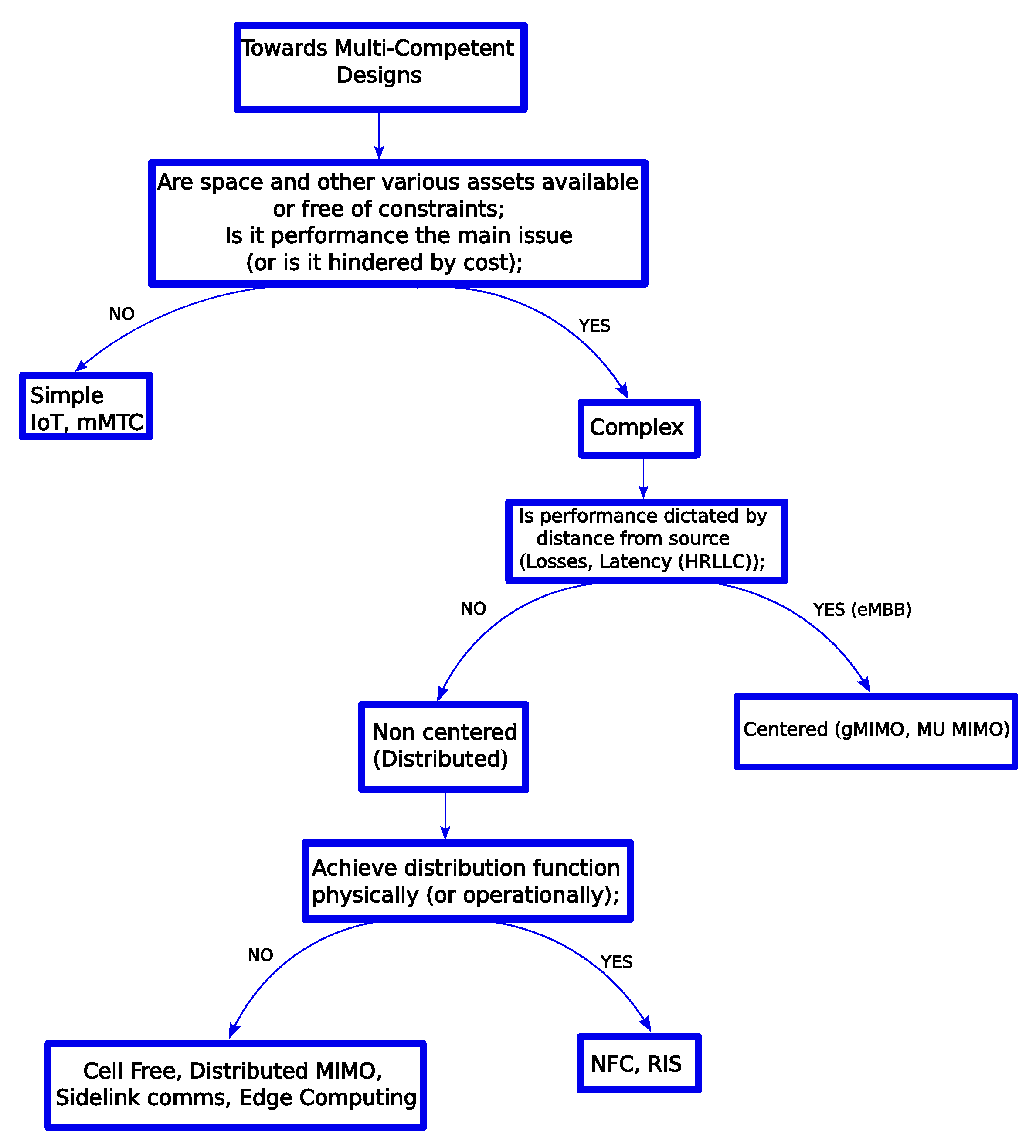
3.1. Reconfigurable Intelligence Surface (RIS)
A highly promising and rapidly emerging technology for enabling ultra-high-throughput communication in the mmWave spectrum and for decoupling wireless communication KPIs from strict dependence on Tx-Rx distance is the reconfigurable intelligent surface (RIS). RIS has gained recognition as a key enabler in enhancing wireless networks, especially in the domains of massive MIMO, beamforming, and integrated sensing. The recent literature underscores rapid advancements in RIS architectures, performance optimization techniques, and deployment strategies. RIS encompasses a broad class of passive or active two-dimensional microwave surfaces that can dynamically manipulate incident RF signals [
59]. These surfaces are capable of reflecting, diffracting, amplifying, focusing, or steering electromagnetic waves. The resulting directive beams help address the fundamental limitations of mmWave bands, such as high free-space path loss and poor penetration through obstacles.
What distinguishes RIS from comparable technologies such as transmitarrays, reflectarrays, or frequency-selective surfaces is its ability to electronically reconfigure its electromagnetic properties in real-time [
59]. For example, an RIS installed on the exterior of a building and configured as a reflectarray can dynamically redirect incoming mmWave signals toward a targeted receiver at the optimal frequency and angle, thereby improving link quality and overall system performance. An example of such a scenario is illustrated in
Figure 3. This transformative potential has sparked significant research interest and innovation in RIS development. A sharp rise in related publications highlights this growing attention [
59,
60,
61,
62,
63,
64,
65,
66,
67,
68,
69]. For instance, in [
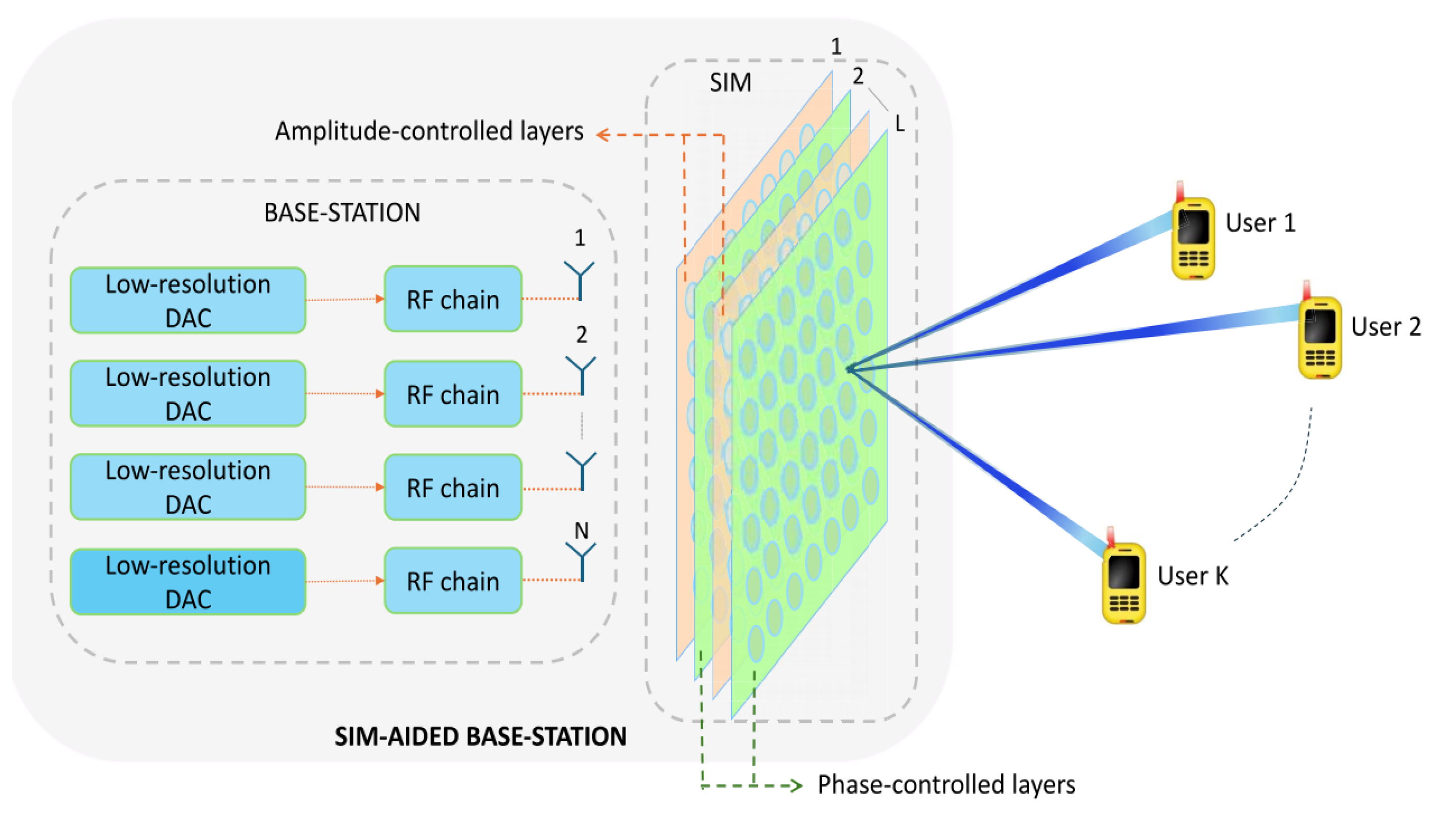
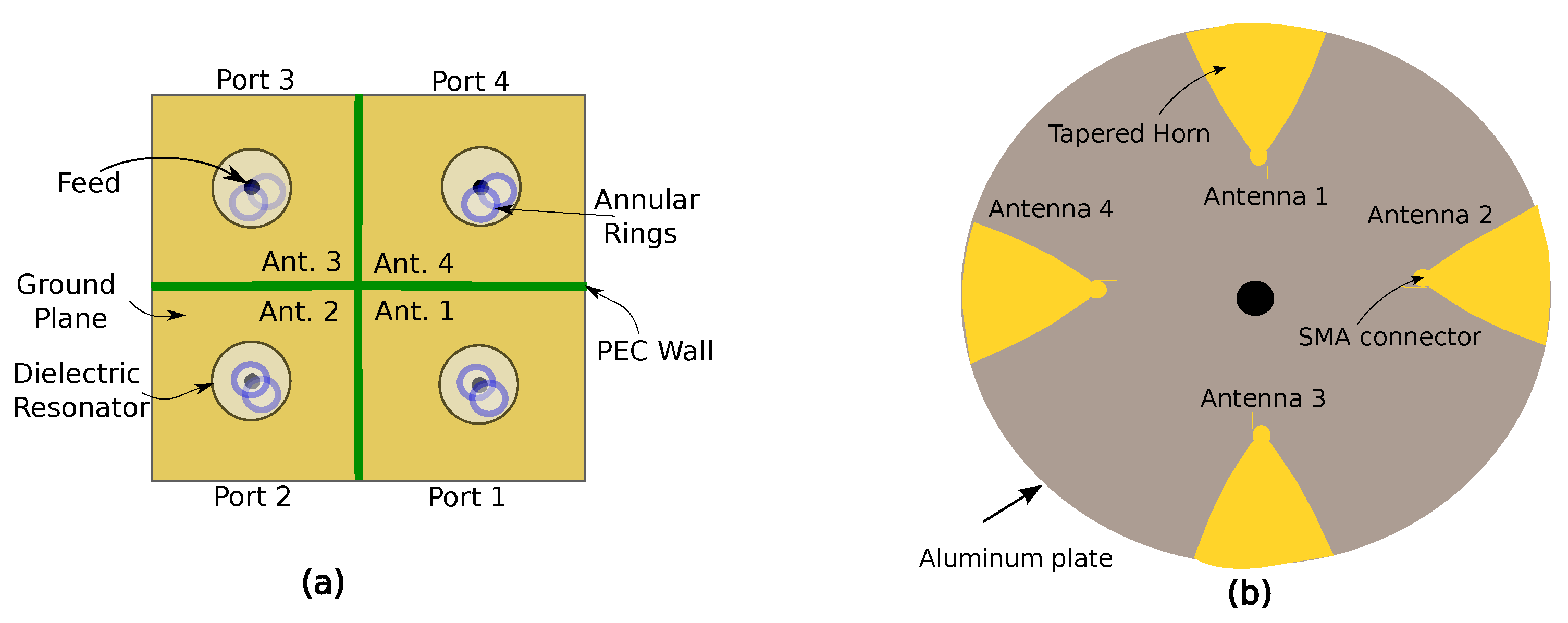
70], the performance of a double-stacked intelligent metasurface integrated into massive MIMO systems is explored. This configuration, depicted in
Figure 4, effectively enhances spatial diversity, thereby improving communication reliability and throughput.
A variety of innovative RIS architectures and applications have been explored in the recent literature, further highlighting the versatility and potential of this technology in next-generation communication systems. In [
71], a simple stacked metasurface architecture with reconfigurable amplitude and phase is utilized to optimize downlink beamforming, significantly improving signal quality in multiuser environments. Active RIS with discrete phase shifts is examined in [
72], demonstrating enhanced spectral efficiency in communication systems. Hybrid RIS configurations designed for integrated sensing and communication are presented in [
73], underscoring the multifunctionality of RIS in future network paradigms. A location-driven beamforming strategy tailored for RIS-enabled near-field communications is proposed in [
74], where beam patterns are dynamically optimized based on user position data to improve connectivity in dense urban settings.
Deployment challenges in complex cellular networks are addressed in [
75], which introduces a frequency-dependent RIS model applicable to multiband, multicell MIMO networks. In [
76], the integration of RIS with spatial modulation is explored to enhance antenna selection for vehicular communications, leading to improvements in link robustness and data rate performance. Furthermore, ref. [
77] presents a transparent, graphene-based RIS operating in the THz band for 6G systems, an innovative design that demonstrates the promise of advanced materials for supporting ultra-high-frequency communications. Despite these advances, several key challenges must be overcome to enable commercially viable RIS deployment. These include optimizing energy efficiency and scalability, refining real-time electronic control mechanisms, and addressing practical concerns such as cost, power consumption, and seamless integration with existing communication infrastructure.
Table 1 lists some notable RIS works that span both passive and active architectures across a wide frequency range from sub 6 GHz to the terahertz band. The table summarizes key characteristics including the type of RIS (passive, active, or hybrid), the number of elements, physical dimensions, underlying manufacturing technology, and operating frequency range, as well as some reported performance metrics.
3.2. Multiple-Input Multiple-Output (MIMO)
In recent years, the term
MIMO has dominated the scientific discourse, promising to address the inherent losses of mmWave communication. However, strictly speaking, this is a widespread misconception, as it is the directional antenna beams that mitigate mmWave losses through their high gain, not merely the multiple ports of the antenna array. Among its key advantages, massive MIMO’s ability to significantly enhance channel capacity stands out [
78]. The term “massive” refers to the inclusion of a large number of antenna elements in the system, often exceeding hundreds and potentially reaching thousands [
79]. This extensive array of elements forms the foundation for robust adaptive techniques aimed at mitigating noise and boosting received signal power. Furthermore, beamforming has become an integral component of MIMO systems, improving system gain and overall performance. Currently, MIMO systems typically employ configurations such as sub-arrays with
antenna elements, particularly in the sub-6 GHz range, where physical size and system complexity remain limiting factors [
80].
MIMO technology leverages multipath communication, exploiting the diverse propagation paths of RF signals to increase channel capacity. This phenomenon is more pronounced in the lower microwave frequency bands (e.g., sub-7 GHz) than at mmWave bands. Notably, multipath dominates at sub-7 GHz, while direct line-of-sight (LOS) is the principal link at mmWave frequencies. MIMO increases capacity by processing distinct signals through transceiver modules, transmitting them from individual elements or subarrays within an antenna array, and subsequently applying post-processing at the receiver to reconstruct the transmitted data. The efficiency of this process is heavily dependent on the algorithms that encode and decode signals based on the channel’s characteristics [
78]. Consequently, a significant body of research focuses on developing advanced algorithms and adaptive techniques to optimize MIMO system performance. One critical challenge is the requirement for real-time processing to accommodate the dynamic nature of the wireless environment. This necessitates continuous monitoring of the channel’s characteristics and frequent updates to the channel matrix for each frequency component to ensure seamless operation. Massive MIMO’s capacity to adapt to changing environments and enhance communication reliability makes it an indispensable technology for next-generation wireless networks. However, appropriate topologies combining MIMO and beamforming must be exploited to address the challenges of mmWave frequencies effectively.
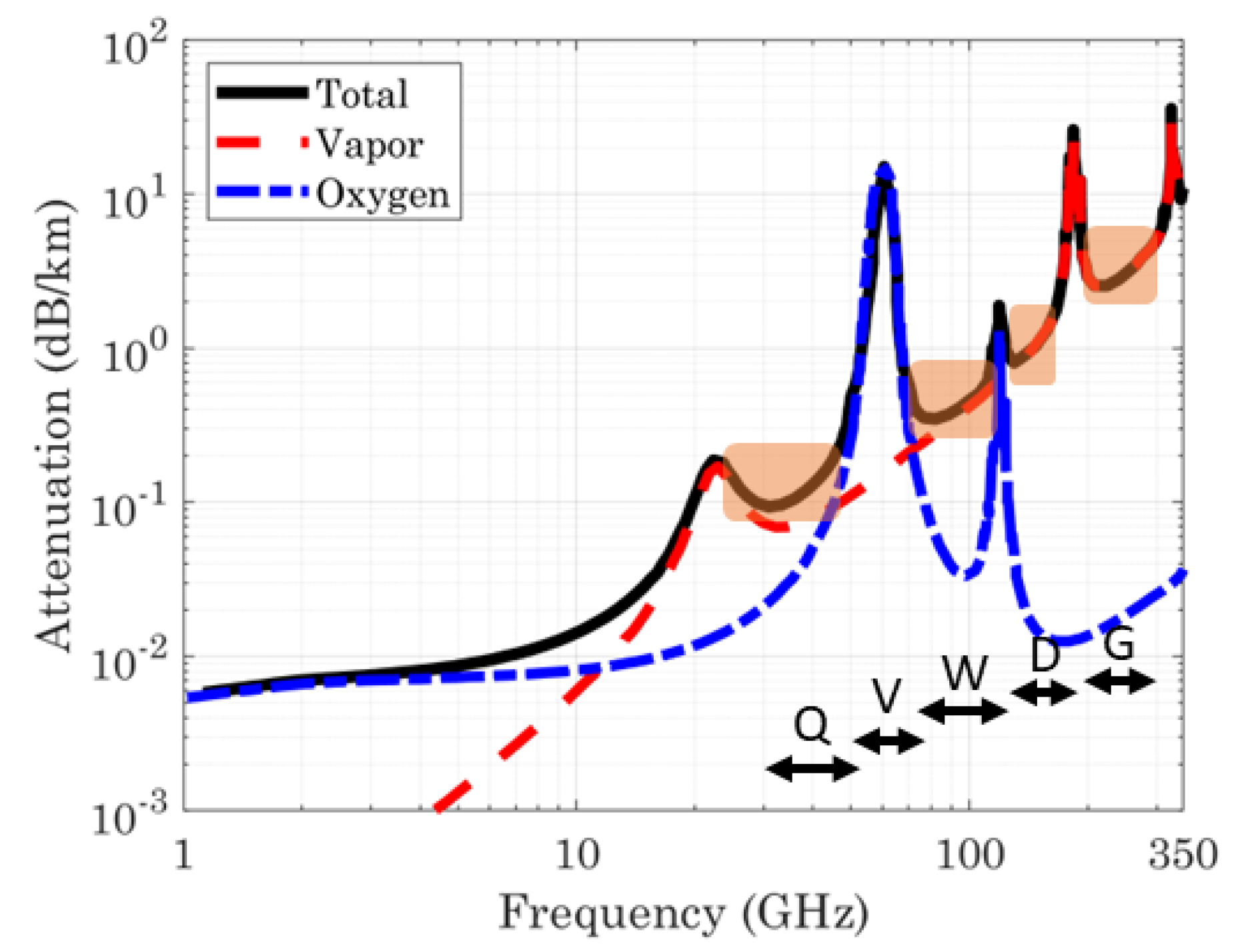
A commonly cited advantage supporting the development of massive MIMO systems or massive element arrays at mmWave frequencies is the relative ease of fabricating antenna arrays with hundreds or even thousands of elements within a compact space, enabled by the short wavelengths at these frequencies [
79,
81,
82,
83,
84,
85,
86]. However, this advantage is counterbalanced by a critical limitation. Specifically, the primary benefit of MIMO, its ability to exploit multipath propagation, is significantly diminished at mmWave frequencies due to increased free space path loss and substantial attenuation from atmospheric gases and water vapor (
Figure 2). To compensate for these losses, antenna systems must achieve considerably higher gain, as the available power is inherently constrained at these frequencies. This requirement necessitates the use of beamforming techniques, which focus energy along a single LOS propagation path. While effective in overcoming propagation challenges, beamforming largely eliminates the ability to capitalize on multipath diversity, which is a key advantage of MIMO technology at lower frequencies. Consequently, at mmWave frequencies, the potential benefits of massive MIMO in harnessing multipath propagation are significantly diminished.
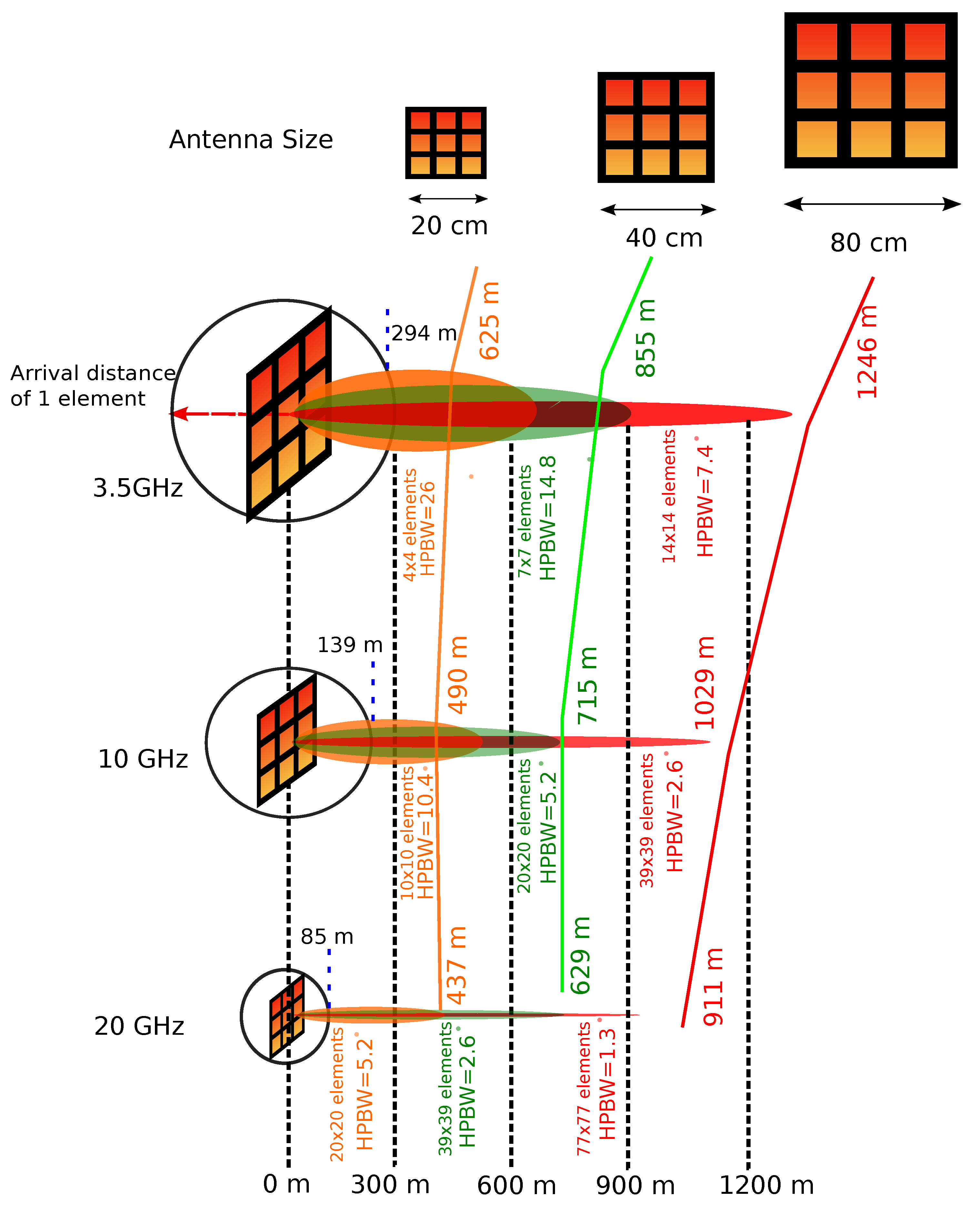
The complex interrelation between beamforming and MIMO at mmWave frequencies is elaborated by NTT-DOCOMO [
87], which refers to “user and spatial multiplexing of massive-element antennas”. An indicative diagram (
Figure 3) illustrates how the number of elements increases with the square of the frequency ratio, while the overall array size remains approximately constant.
For instance, at a range of approximately 490 m, a square array of size comprises elements at 10 GHz, or elements at 20 GHz. Although the physical array size is retained, the dramatic increase in element count introduces major challenges in beamforming or antenna feeding network design. A practical solution lies in hybrid beamforming. In the example above, each subarray could employ an analog beamforming circuit, e.g., switched-beam Butler, Nolen, or Blass matrices, while MIMO-based user multiplexing could be handled by an equal number of subarrays, each driven by a separate RF chain.
Another major challenge in implementing massive MIMO systems is the enormous complexity introduced by managing the envisioned millions of antenna elements. Controlling such a vast number of elements requires numerous fully controllable RF transceiver chains, each of which must be monitored and dynamically adjusted in real-time. Essentially, the challenge lies in managing and optimizing the individual radiated beams, typically achieved by controlling the excitation current of each antenna element in terms of amplitude and phase. However, some analog beamforming techniques, such as switched-beam systems, offer a more practical approach by simplifying control through the selection of the appropriate transmit/receive (Tx/Rx) beamforming network port. To address these issues, various research groups have proposed hybrid MIMO architectures that combine analog and digital signal processing, aiming to minimize the number of required RF chains without compromising performance. Despite these theoretical advancements, practical implementations of massive MIMO systems for mmWave frequencies remain scarce. The majority of published work focuses on simulations, with emphasis on developing and testing advanced algorithms for MIMO system optimization. The introduction of artificial intelligence (AI) and machine learning (ML) is expected to play a crucial role in addressing beam management challenges, offering enhanced adaptability and real-time optimization. However, the physical fabrication and experimental validation of such systems present significant challenges. These stem from intricate design requirements, complex manufacturing processes, and the demanding testing environments needed to ensure accurate performance validation.
Traditional microwave testing methods become impractical due to the extremely high number of ports. Thus, conductive path approaches involve high complexity and require excessive effort. In the sub-7 GHz band, these issues are reliably addressed through over-the-air (OTA) testing approaches. However, in the mmWave bands, the number of ports is expected to remain relatively small, making testing methods involving conductive techniques (e.g., cables or waveguides) potentially more practical and accurate.
3.3. Beamforming Networks at mmWaves and THz
The demand for high-gain antennas operating at mmWave frequencies has surged, driven by the need to extend the range of communication links in these bands, while meeting the performance requirements of 6G networks. As 6G aims to deliver ultra-high data rates, extreme coverage and reliability, and massive connectivity, beamforming has emerged as the most effective method for achieving these goals: not only enhancing signal gain, but also enabling dynamic real-time beam steering, thus optimizing link quality, reducing interference, and supporting massive connectivity. Additionally, 6G networks require highly adaptive and intelligent beamforming solutions that leverage AI and ML to predict user movement, optimize spectral efficiency, and manage complex multi-antenna deployments. This adaptability makes beamforming a cornerstone technology in mmWave communication systems, ensuring robust and energy-efficient wireless transmission in next-generation networks [
88,
89].
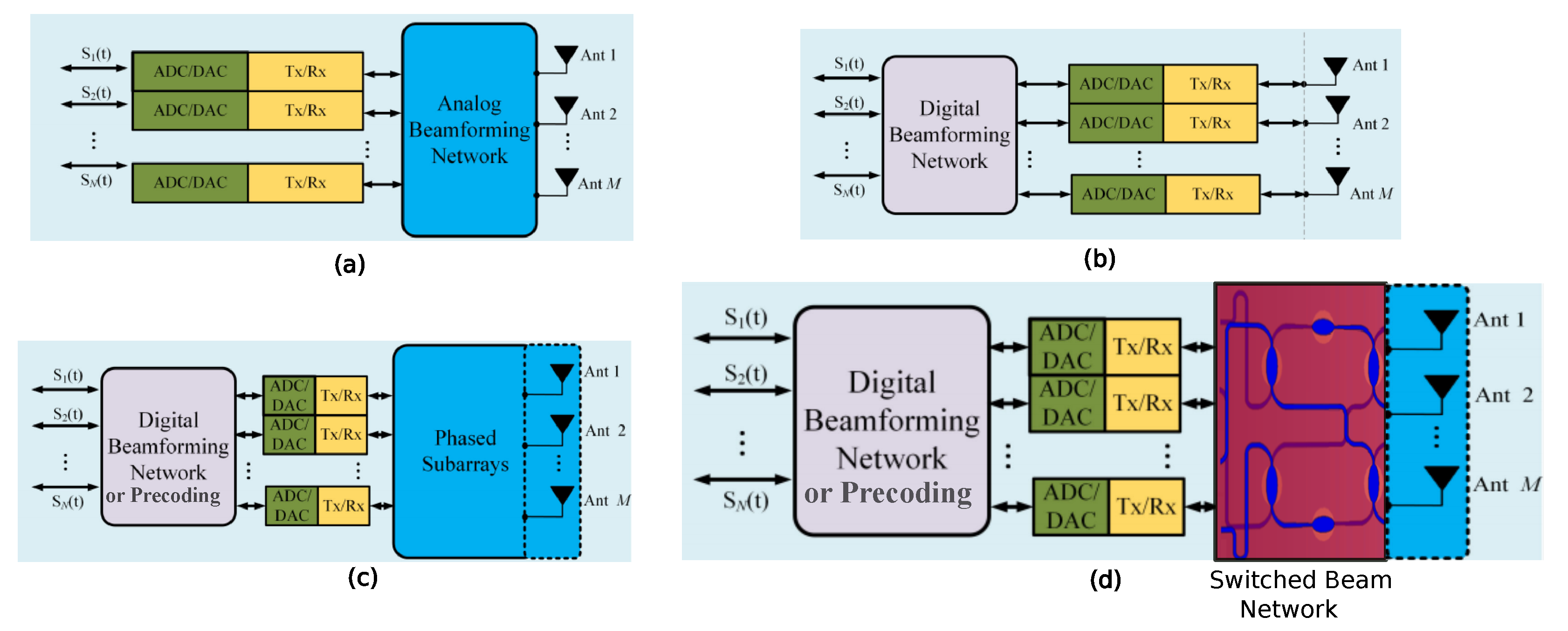
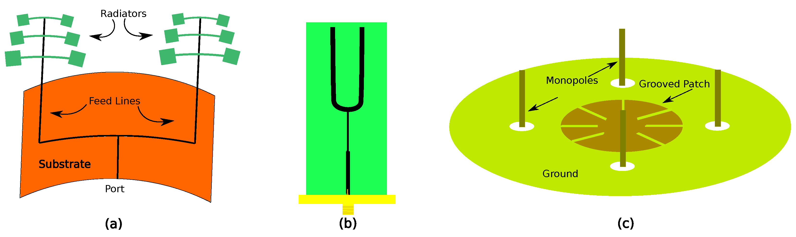
Beamforming relies on two key components: a phased array (linear, conformal cylindrical, or planar) and a feeding network [
23]. The phased array consists of multiple antenna elements, while the beamforming feeding network provides each element with the necessary signal characteristics, specifically, the amplitude and phase of the excitation current, to shape and direct the beam. Historically, fully passive beamforming networks were used (see
Figure 5a). Switched beam networks, such as Butler matrices, Nolen matrices, Blass matrices, and Rotman lenses, introduced predefined phase shifts or time delays through fixed excitation ports [
90,
91,
92,
93,
94,
95]. While these systems were effective in early applications, their inherent inflexibility and lack of adaptability limited their functionality in dynamic environments. Particularly in the sub-7 GHz band, where multipath dominates and is exploited through MIMO, digital beamforming is preferably utilized, while matrix-switched beams are rarely adopted. However, these matrix-based beamforming networks (BFNs) have the potential to be effectively utilized in mmWave networks, particularly when modified to function as hybrid digital–analog beamformers, as indicatively presented in
Figure 5d. By integrating multiple matrices, it is possible to construct three-dimensional beamforming networks capable of optimally steering highly directional radiation beams [
96,
97].
To understand the beamforming effect, we conduct the following study. Assuming a total transmission power of
dBm from a 5G base station [
98], and a received power of
dBm for a conventional mobile phone with full reception [
99], we consider communication in the
GHz, 10 GHz, and 20 GHz bands. The mobile phone antenna gain is assumed to be
dBi. To maintain communication at the same distances across these frequency bands, we analyze different planar antenna array configurations at the base station: (1) at
GHz, we consider
,
, and
arrays; (2) at 10 GHz, we consider
,
, and
arrays; and (3) at 20 GHz, we consider
,
, and
arrays. The coverage estimation is based on the Friis transmission formula,
, where
is the received power at the mobile phone in dBm,
is the transmit power from the base station in dBm,
is the base station antenna gain in dBi,
is the mobile phone antenna gain in dBi,
represents penetration losses in dB,
accounts for shadowing and fading losses in dB, and
denotes path losses in dB, given by
, where
d is the distance in km, and
f is the signal frequency in MHz. The base station antenna gain is calculated using the maximum directivity of a planar array, assuming total efficiency
; thus,
, where
, with
being the effective area [
100]. For a realistic scenario, we incorporate penetration losses of
,
, and
dB at
, 10, and 20 GHz, respectively, as reported in [
101]. Similarly, we consider shadowing and fading losses of 6, 7, and 8 dB at
, 10, and 20 GHz, respectively, based on findings from [
102,
103,
104].
Figure 6 shows the range achieved by each antenna configuration under these conditions.
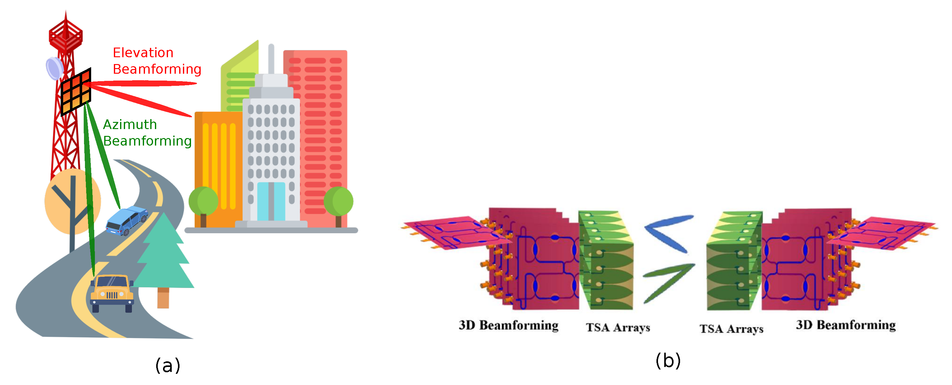
An example of a 3D beamforming topology [
105] is illustrated in
Figure 7, and it is utilized to enhance system capacity and efficiency by enabling precise transmit and receive functions with narrow beams in both azimuth and elevation angles. This analog 3D beamformer is constructed using a stack of vertical beamformers (BMs), which are driven by either a single horizontal BM or a stack of horizontal BMs. To achieve ultra-wideband performance, the planar array is composed of planar-printed Vivaldi antenna elements, ensuring high directivity and efficient spatial coverage. Both adaptive phased-array beamforming and switched beamforming will play a crucial role in coverage extension in 6G non-terrestrial networks (NTN), enabling seamless connectivity across air, sea, and space. This involves the integration of LEO (low Earth orbit) satellites, GEO (geostationary) satellites, and HAPS to provide global coverage. Since LEO satellites traverse the sky at high speeds and for short durations (up to 30 min), real-time beam steering is essential to continuously track mobile ground terminals, ensuring stable and seamless connectivity. Scalable, reconfigurable, and large antenna arrays are required to serve multiple ground terminals simultaneously. A relevant example of this is a 1024-element SATCOM phased array, as discussed in [
106]. The key challenges for phased-array beamformers will be high power consumption and increased computational complexity, especially in large-scale systems, as well as cost-effective implementation, particularly for LEO terminals that require real-time tracking. On the other hand, less complex switched beam beamformers can be effectively deployed in GEO satellites to cover vast geographic areas with predefined beams and in HAPS platforms to provide extensive ground coverage without requiring continuous steering, thereby minimizing power consumption. They are also well suited for backhaul communication between terrestrial networks and NTN. A 3D beamformer featuring a
(256 element) array or larger, powered by a stack of multiple beamform modules similar to the design shown in
Figure 7b, is expected to significantly improve coverage and performance for 6G networks. Although the main issue in extreme coverage extension is long-distance signal propagation, particularly in NTN where signals must travel thousands of kilometers while maintaining low latency and high reliability, 3D beamforming is essential for handovers between terrestrial 6G networks and NTN systems, significantly enhancing spectral efficiency. Additionally, it enables high-gain directional beams, optimizing signal strength and ensuring efficient long-distance communication in NTN environments. To integrate 3D beamformers into the aforementioned platforms, a miniaturized and compact design with enhanced performance accuracy is essential for optimal efficiency and seamless deployment.
The introduction of tunable and reconfigurable components, such as phase shifters [
107], attenuators [
108], and SPDT switches [
109], marked a significant step forward. These devices enabled precise control over the phase and amplitude of the excitation currents feeding each antenna element, while the SPDT switches enabled dual-port excitation of the beamformer to produce additional beams. However, their use in mmWave systems is constrained by their high insertion loss and limited tuning ranges, which degrade performance at higher frequencies [
110]. To address these limitations, more advanced beamforming architectures have been developed, including fully digital [
111,
112,
113,
114] and hybrid analog–digital systems [
115,
116,
117]. In a fully digital beamforming network, each antenna element receives a signal that is digitally processed and then converted to an analog signal using a digital-to-analog converter (DAC), as shown in
Figure 5b. This approach provides unparalleled flexibility and precision in shaping the beam. However, at mmWave frequencies, fully digital systems face significant challenges. In general, DACs consume significant power, particularly at high sampling rates (
). The sampling must obey the Nyquist minimum rate
, where
represents the operational channel bandwidth of the received signal. However, complex sampling techniques can be employed to reduce the required sampling rate by half, allowing
. In practical implementations, commercial ADCs and DACs, especially those used in software-defined radio (SDR) applications, often operate at slightly higher sampling frequencies (approximately
for real signals or
for complex (IQ) signals) to ensure optimal performance [
118]. Notably, current 5G systems support channel bandwidths of up to 200 or 400 MHz, whereas 6G is expected to accommodate bandwidths ranging from
GHz to 2 GHz, posing new challenges in power efficiency and signal processing capabilities. The DACs required to generate signals with these requirements must operate at extremely high sampling rates, which can result in substantial power consumption and reduced system efficiency.
Hybrid beamforming networks provide a practical solution for mmWave applications [
113] and are essential for THz frequency bands. By integrating analog and digital processing, these systems efficiently handle the high data rates and massive connectivity demands of 6G while reducing power consumption and hardware complexity [
119]. The signal undergoes initial digital processing before being converted into an intermediate analog form. Subsequent operations, including up-conversion, amplification, and filtering, take place in the analog domain before transmission through the antenna elements, as illustrated in
Figure 5c. By minimizing the number of DACs and leveraging analog signal processing, hybrid architectures achieve an optimal balance among complexity, performance, and energy efficiency, making them well suited for high-frequency applications. However, implementing hybrid beamforming in 6G introduces several challenges. Propagation loss compensation at THz frequencies requires high-gain arrays to maintain reliable communication. The beam squint effect is also an important issue [
120], where the wide bandwidths of THz communications cause beams to shift in different directions at varying frequencies, leading to array gain loss. Furthermore, hardware constraints pose a significant hurdle, as hybrid beamforming in ultra-massive MIMO (or multi-antenna) systems demands managing large numbers of antennas and RF chains, increasing both hardware complexity and power consumption. Lastly, beam management is crucial in dynamic environments [
121], where user mobility and rapid changes in channel conditions require efficient beam alignment and tracking mechanisms to ensure seamless connectivity.
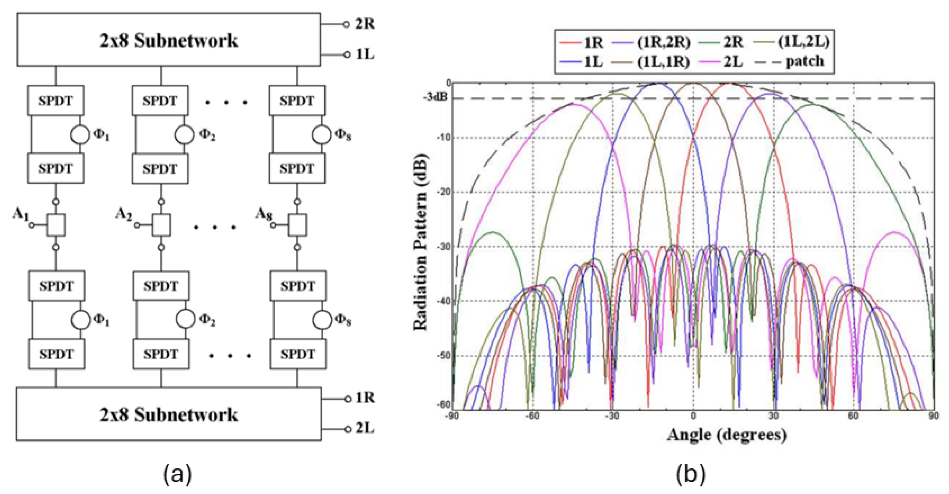
3.4. Angular Coverage
An important issue in mmWave hybrid or switched beam matrix beamformers is related to continuous angular coverage. Specifically, at mmWaves, increased gain is needed to mitigate propagation losses, thus corresponding to narrow beamwidth. When this is successfully achieved, the consecutive switched beams may overlap at very low levels, below
dB. This problem can be mitigated by introducing a group of intermediate orthogonal beams, as suggested by Fakoukakis et al. [
122], which is also shown in
Figure 8. This is achieved by introducing constant-value phase shifters between the Nolen or Butler matrix outputs and the antenna ports, selectable through digitally controlled RF switches. At even higher frequencies, a third or fourth group of additional orthogonal beams may be needed if the radiation pattern of the element is highly directive. As displayed in
Figure 8, a
Nolen matrix can be expanded by introducing an intermediate group of three additional beams, leading to a total of seven beams and improving the overlapping point to
dB.
As future 6G networks adopt larger antenna arrays and operate at higher frequencies, such as the THz band, beamforming will become increasingly complex. To address this challenge, AI, particularly ML, is being leveraged to optimize beamforming strategies, enhancing efficiency, adaptability, and overall network performance [
123,
124]. The optimization process involves several key aspects, including enhanced beam selection, where AI identifies the optimal transmission beam, reducing latency and improving signal quality. Additionally, adaptive beam management allows AI-driven algorithms to enable real-time beam tracking and selection, ensuring seamless communication in dynamic environments. Furthermore, Improved channel estimation leverages AI to predict channel conditions with greater accuracy, enabling more efficient and adaptive beamforming adjustments. However, several challenges must be addressed. One major issue is algorithm selection, as identifying the most suitable AI model for specific beamforming scenarios remains difficult. Another critical concern is security, as AI-based beamforming systems must be safeguarded against adversarial attacks to ensure network integrity and reliability.
The development of 6G technology presents substantial challenges in PCB manufacturing, particularly in ensuring signal integrity and minimizing losses. Advancements in digital and RF systems so far rely heavily on PCB technologies, where transmission lines are typically incorporated into planar or multilayer structures to support seamless integration and high-performance operation. However, at frequencies above 10 GHz, RF propagation through dielectric materials introduces significant losses. In the context of 6G communication systems, where power efficiency is paramount, minimizing transmission and insertion losses in devices is critical. Consequently, alternative transmission line technologies have been explored to address these challenges. One promising solution is substrate integrated waveguides (SIWs), a hybrid technology that combines the advantages of metallic rectangular waveguides and printed transmission lines [
125]. An inevitable requirement for the selection of mmWave transmission lines is to avoid dielectric losses, which are unacceptably high even at microwave frequencies. Additionally, the metallic surfaces must be made perfectly smooth (metal spreading) to minimize current paths, since at mmWaves, the penetration depth is very short. Thus, waveguides based on air or with isolated metallic parts are needed. The trend is to devise waveguides with a planar structure but with air or gap-isolated conductors.
SIWs are fabricated using a dielectric substrate with metalized top and bottom layers and vertical vias along the sides to form a pseudo-waveguide structure. This configuration reduces losses compared to traditional printed lines while supporting higher power handling, all while maintaining the benefits of printed circuits, such as compactness and easy integration [
126]. Despite these advantages, SIWs still suffer from dielectric losses [
127]. To mitigate this issue, air-filled SIWs have garnered significant interest. In these designs, the dielectric propagation medium is replaced by air, resulting in substantially lower losses. However, the fabrication process for air-filled SIWs is more complex, requiring precise techniques to maintain structural integrity and performance [
128,
129].
An even more advanced alternative is the use of full metallic waveguides with internal ridges or grooves [
130,
131,
132]. These waveguides offer minimal propagation losses and compact designs suitable for mmWave frequencies.
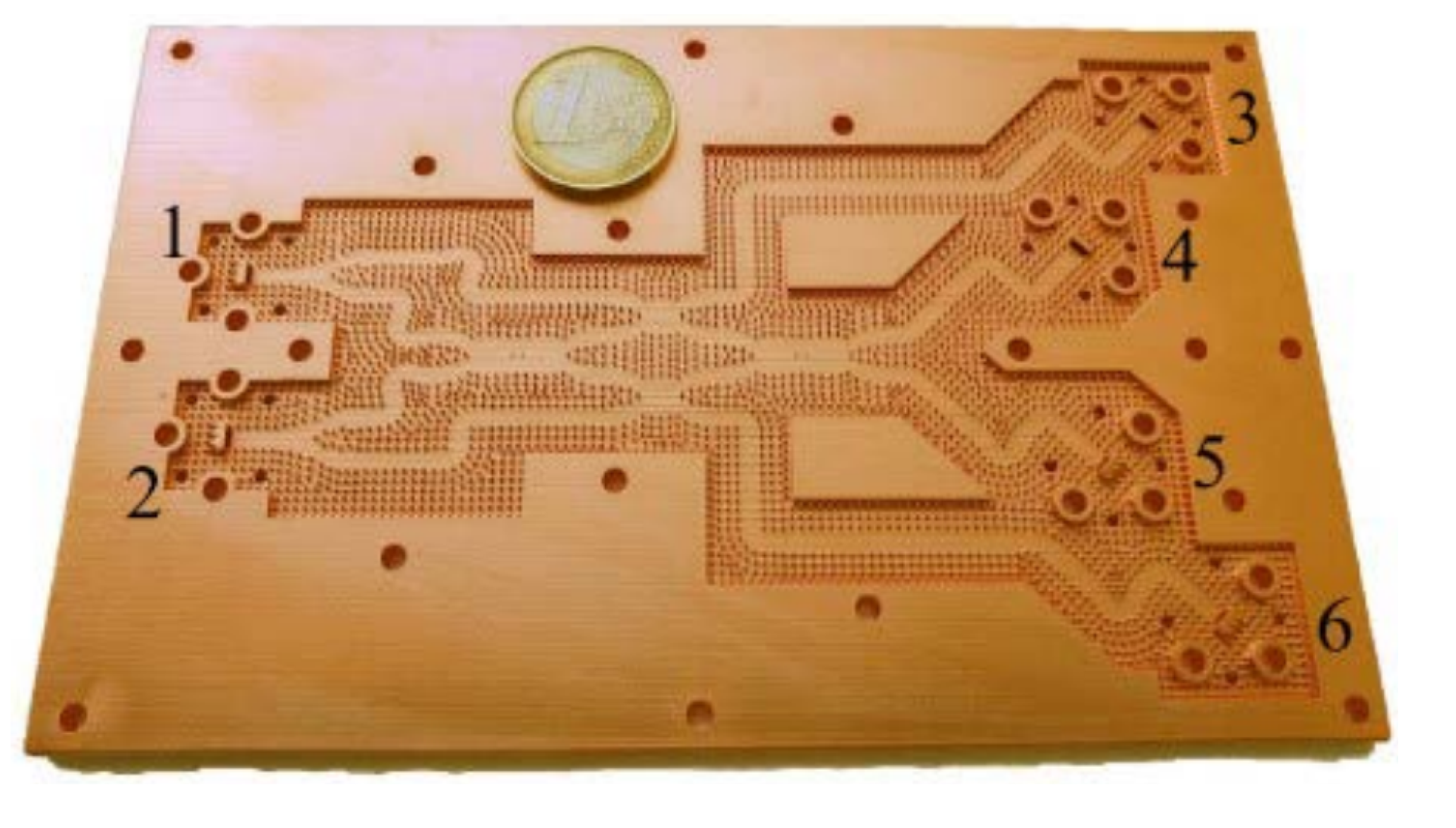
The feasibility of such structures has been enabled by breakthroughs in micromachining technologies, which allow the precise milling of metallic blocks into intricate and sophisticated geometries. An example of a groove gap waveguide 3D beamformer fabricated using additive manufacturing is shown in
Figure 9. By leveraging these innovations, passive beamforming networks for mmWave applications can be realized with ridge, groove, inverted microstrip, or microstrip ridge waveguides, which introduce negligible RF signal losses. This significant reduction in losses enhances the overall efficiency of the communication system, aligning with the stringent power efficiency requirements of 6G technologies. The development of mmWave beamformers, whether based on switched-matrix or hybrid topologies, has already garnered significant interest from researchers worldwide. However, progress in this area has been relatively slow compared to the rapid pace of 5G and anticipated advances of 6G.
Table 2 lists some notable work on beamforming network implementations, highlighting various architectures such as Butler matrices, Nolen matrices, and fully digital phased arrays. For each case, the beamforming type, frequency range, physical dimensions, fabrication technology, and number of supported beams are summarized to provide a comparative overview of analog, digital, and hybrid approaches across different platforms.
3.6. Techniques for Reconfigurable RF Front-End Systems and Antennas
Following the emerging trends of low-cost, frequency-agile, and reconfigurable communication systems for 6G, the development of novel tunable devices is essential. Reconfigurable RF front-end will play a pivotal role in the miniaturization and simplification of future base stations. With 6G expected to unify various licensed spectra, including satellite communication, terrestrial networks, radar systems, and more, there will be a significant demand for wideband systems, particularly in base stations. The development of such wideband systems poses considerable challenges, as it further complicates the design and operation of RF transceivers. To address this, an effective strategy is the design and implementation of tunable microwave devices and antennas. These devices would enable the dynamic adjustment of system response based on the utilized frequency band, reducing complexity and minimizing insertion losses particularly at mmWave frequencies. In microwave technology, tunability refers to the electronic control of different characteristic of a device. For example, in antennas, the ability to control the radiation pattern and operation frequency is a highly valuable asset.
Traditionally, the most widespread technique for introducing electronic control in microwave systems involves the use of semiconductors, such as PIN diodes, varactor diodes, or transistors acting as switches [
145,
146]. Typically, these switches connect or disconnect specific elements from the main structure of the device, or they introduce variable capacitance to modify its properties. For instance, a continuously tunable SIW filter was demonstrated using varactors integrated into a resonator patch [
147], and a 1-bit reconfigurable metasurface was proposed in [
148]. A tunable filtenna for X band applications were proposed in [
149] where a novel superstrate-loading technique was applied permitting the frequency control using only one varactor. The measured antenna’s tunability reached
, providing more than 20 dB out-of-band radiation suppression. As illustrated in
Figure 10a, a PIN diode is employed between the arms of a Jerusalem cross, enabling the metasurface to switch between transmission and reflection modes.
However, a significant limitation of such tuning mechanisms lies in the discrete nature of their tuning states, which can restrict applications or require a large number of switches to achieve finer control [
150,
151]. The increased number of switching elements also leads to higher power consumption, particularly for diodes, as they require a bias voltage for their operation. Thus, minimizing the number of diodes is an active area of research. Moreover, as a two-terminal device, the PIN diode shares a single physical point for both the control port (biasing) and the RF signal. This dual use complicates the design of the biasing network, which must integrate the DC and RF signals while ensuring proper isolation between them. Designing effective solutions to these challenges is crucial for advancing reconfigurable microwave technology.
On the other hand, RF microelectromechanical systems (MEMS) offer superior isolation, lower insertion losses, and higher power-handling capabilities compared to traditional switching mechanisms [
152]. Due to their compact size (typically smaller than 1 mm), MEMS devices are particularly attractive for miniature frequency-reconfigurable antennas [
152,
153], where the effective length of the antenna is adjusted by adding or removing parts of the radiating element. Recently, significant research efforts have focused on developing MEMS for mmWave bands, leveraging their advantages in the design of novel variable phase shifters [
154] and attenuators [
155] for beamforming networks [
156,
157]. Moreover, a new type of MEMS-based linear RF switches was fabricated and tested in [
158] (see
Figure 10b), demonstrating operation over a wide frequency range from 20 GHz to 110 GHz, thereby enabling high scalability for future communication systems. Despite these advantages, MEMS presents low switching speeds and challenges in integration.
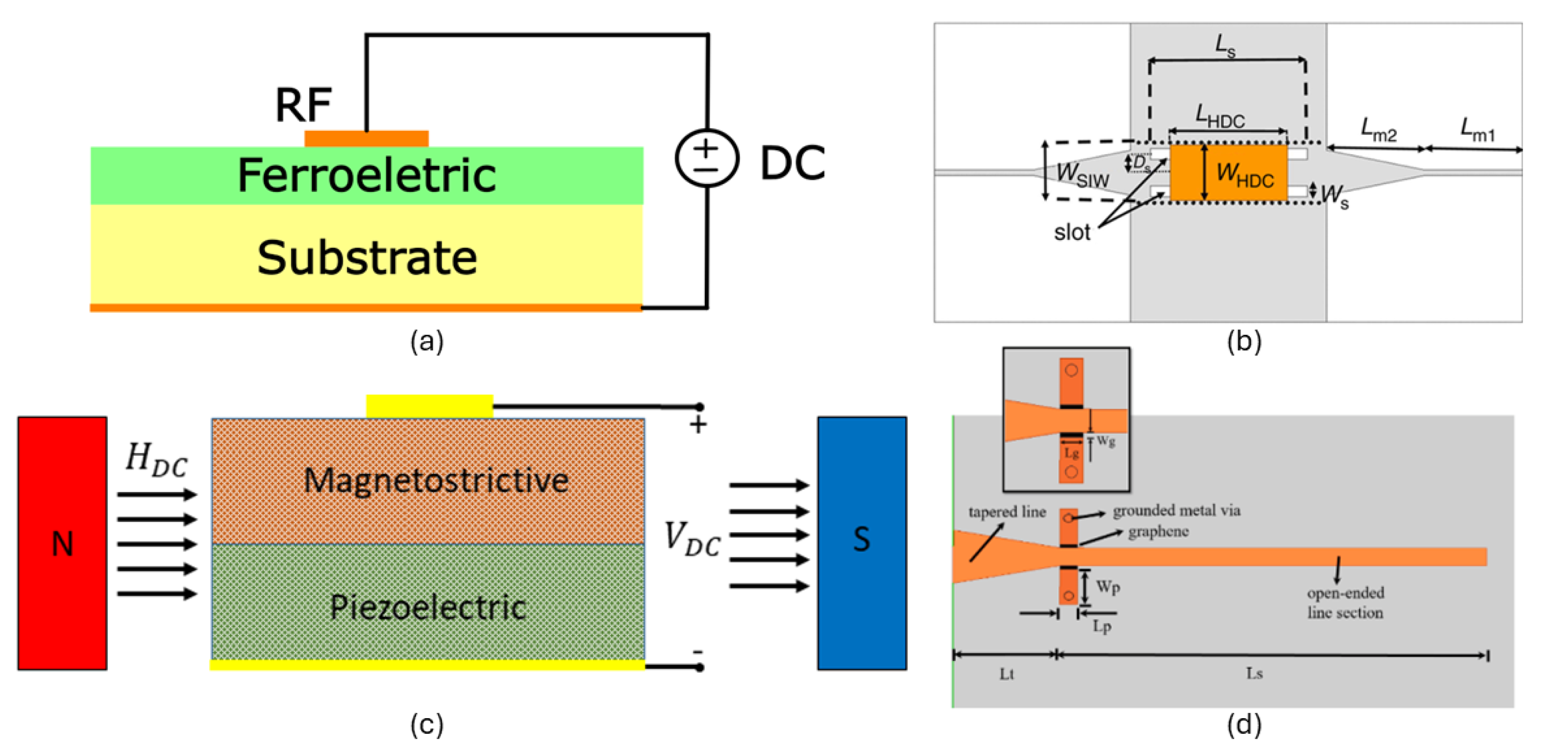
The previously mentioned approaches involve external devices integrated into the structure. An alternative solution is the use of tunable materials, which exhibit properties that can be varied when biased with an appropriate DC field. Two of the most widely researched tunable materials are liquid crystals/ferroelectrics [
159] and ferrites [
160]. Liquid crystals and ferroelectrics enable permittivity tuning with applied voltage (see
Figure 11a), while ferrites allow permeability tuning through the application of a DC magnetic field. These materials are generally considered cost-effective and technologically promising for mmWave frequencies, with applications spanning RIS [
161,
162], filters [
163,
164], tunable phase shifters [
165,
166] and reconfigurable phased arrays [
167,
168], among others. An example of a reconfigurable antenna is depicted in
Figure 10f. However, at higher and particular at mmWaves frequencies, these materials face several challenges, such as increased insertion losses, reduced efficiency [
168], higher power consumption, and the requirement for complex biasing networks [
169]. To mitigate the increased losses, thin film ferroelectrics such as
and its composites [
170] were utilized for the development of RF surface mount capacitors [
171], RIS [
172], and tunable phase shifters [
173]. For ferrites, the switching speeds are limited by the capabilities and the bulkiness of the electromagnets employed. An example of a
phase shifter with ferrite slab developed utilizing SIW technology is presented in
Figure 11b.
To address these issues, composite multiferroics have recently been proposed as an alternative solution. These materials combine the advantages of both ferroelectrics and ferrites, offering potential improvements in tunability [
174]. The working principle of composite magnetoelectric/multiferroic materials can be described as follows: When an electric field is applied to a piezomagnetic material, the microscopic electric dipoles shift, causing mechanical deformation. This deformation is transmitted across the interface to the magnetic material, where a similar effect, such as magnetostriction or piezomagnetism, takes place, leading to an overall macroscopic magnetization. This process, known as converse magnetoelectric coupling, results in the modification of the material’s magnetization by an external electric field, as seen in
Figure 11c. Conversely, the direct magnetoelectric effect occurs when a magnetic field is applied to a magnetostrictive material, generating voltage or polarization due to strain-induced effects in the piezoelectric component. Some popular piezoelectric materials are PZT, barium strontium titanate (BST), and lithium niobate, while for magnetostrictive, there are YIG, Terfenol, Metglas, NFO, and Galfenol. Despite these advancements, the tuning range of currently available tunable microwave devices remains limited due to the low electromechanical coupling [
175,
176,
177,
178,
179]. Another challenge is that the strong magnetostrictive materials such as Metglas and Terfenol are highly lossy at microwave frequencies, making them unfit for such applications.
For sub-THz and THz applications, graphene has been extensively exploited due to its intrinsic property of tunable conductivity via applied chemical potential [
180,
181,
182]. Yasir et al. [
180] proposed a tunable phase shifter where graphene alters both the amplitude and phase response of the device, as shown in
Figure 11d. Another key application area is nano-antennas, where conventional metals such as copper and gold approach their plasma frequency and become extremely lossy, rendering them inefficient as radiating elements [
183]. Consequently, graphene-based optical nanoantennas are widely integrated into optoelectronic devices for plasmonic applications and have become a focal point of research worldwide [
184,
185].
Furthermore, integrating graphene metal hybrid antennas [
186,
187] into optoelectronic platforms enables the realization of versatile photonic systems. Various techniques for frequency tuning [
188] and active modulation [
189] of optical properties particularly via in situ control using external electric fields have been explored. Additionally, multiple approaches for beam scanning and reconfigurable beam control have been proposed, including reflectarrays [
190] and leaky-wave graphene antennas [
191]. However, the relatively low conductivity of graphene introduces significant losses, which degrades device efficiency. Therefore, innovative methods are required to fully harness the potential of multiferroic and graphene-based structures for RF applications. To mitigate losses at mmWave frequencies, particularly for RIS applications, novel approaches utilizing the mechanical control of individual array elements have emerged [
192,
193,
194,
195]. These methods employ rotary actuators [
192,
193], electromagnets [
194] (as shown in
Figure 10c), or electric motors [
196] for actuation. Similar to MEMS, such mechanical elements often function as switches with discrete states [
195]. One major advantage is their simplified biasing networks compared to semiconductor-based solutions. Nonetheless, these systems face inherent limitations due to the physical response times of mechanical actuators and electromagnetic mechanisms [
193,
194,
196]. Additionally, the incorporation of larger mechanical components, as demonstrated in [
194,
196], can lead to bulky structures, which restrict their integration in compact base stations or large-scale RIS implementations. Ongoing and future research aims to overcome these constraints and enhance the practicality and scalability of mechanically reconfigurable RF systems.
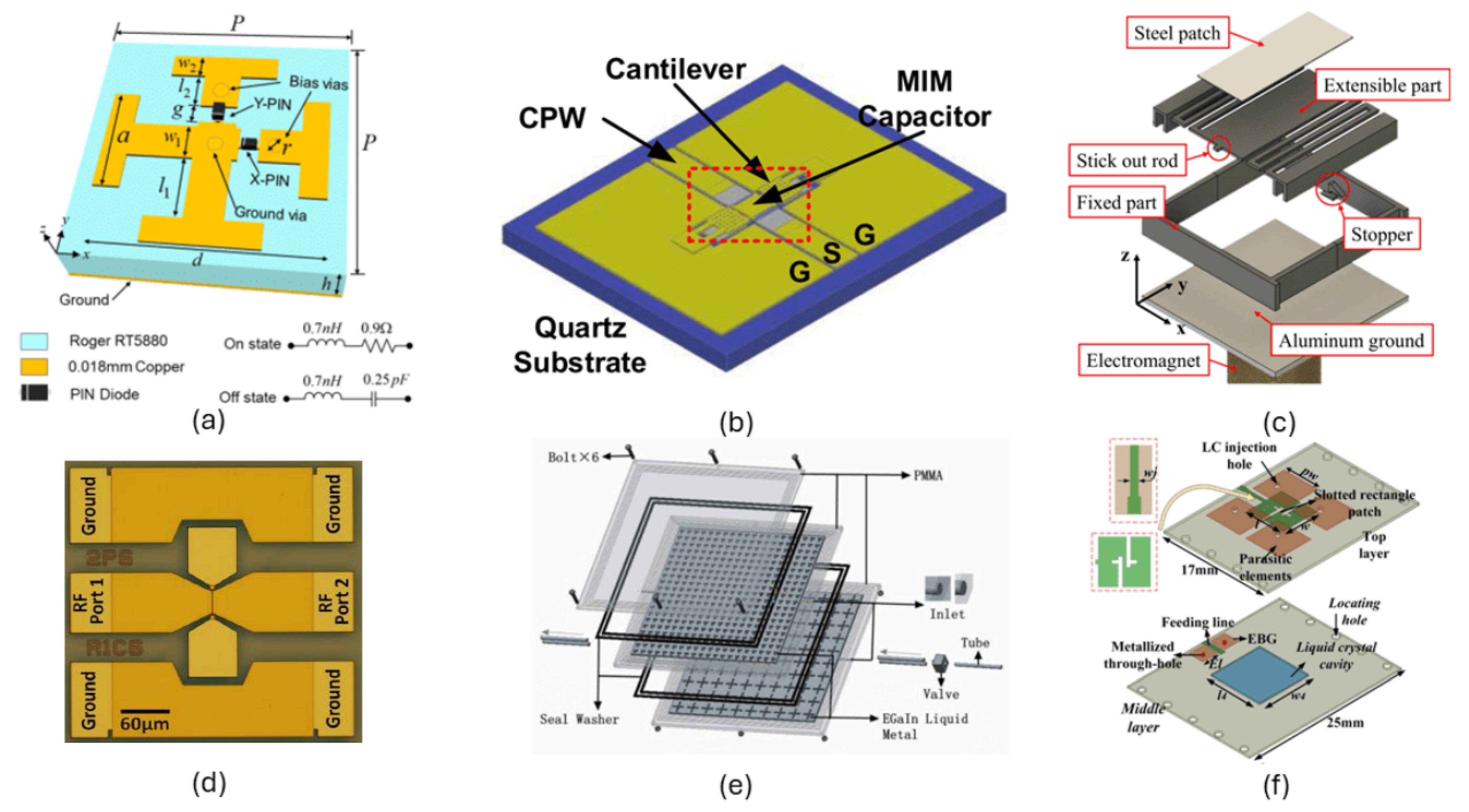
Figure 10.
Examples of reconfigurable devices with (
a) PIN diodes at Jerusalem cross unit cell [
148], (
b) MEMS as mm-waves switches [
158], (
c) an electromagnet-controlled element with varying height for RIS [
194], (
d) a PCM RF switch using coplanar waveguide technology [
197], (
e) a liquid metal double-layer FSS [
198], and (
f) a liquid crystal-based antenna [
199].
As noted, mechanical RF components currently deliver exceptional performance and reliability. However, they are often bulky, expensive, and not easily scalable despite outperforming semiconductor-based switches in terms of RF characteristics due to reduced leakage and parasitic effects at mmWave frequencies [
200]. While RF-MEMS offer superior RF performance, they typically require high DC actuation voltages and specialized packaging, which limits their integration into compact systems.
To address the growing demand for miniaturized mmWave devices, particularly for handheld and IoT applications, phase change materials (PCMs) have emerged as a promising alternative for RF switching [
201,
202]. PCMs can exhibit resistance changes spanning five orders of magnitude when subjected to nanosecond-scale voltage pulses, making them ideal for low-loss, high-speed switching at microwave and mmWave frequencies [
201]. The two most widely studied PCMs are vanadium dioxide (
) and germanium telluride (
) [
202]. Their operation relies on reversible changes in the crystal structure of chalcogenide materials between amorphous (high-resistivity) and crystalline (low-resistivity) states, typically triggered by thermal pulses.
This switching mechanism mirrors that of conventional electronic switches, enabling the development of fundamental PCM-based RF components such as SPDT, SP4T, and SP8T switches [
203,
204,
205]. An optical image of a PCM-based RF SPDT switch fabricated on coplanar waveguide technology is shown in
Figure 10d. By combining SPDT elements into more complex topologies, researchers have demonstrated advanced PCM-enabled systems, including crossbar switching matrices [
206], tunable filters [
207], tunable attenuators [
185], and reconfigurable antennas [
208]. Despite their significant potential, PCM-based devices face challenges that have limited their widespread commercialization, including moderate power handling, limited switching speed, and restricted cycling endurance [
209]. Continued research is needed to address these issues and fully realize PCM-based RF switching technologies.
In recent years, liquid metals have emerged as a compelling solution for reconfigurable and flexible RF circuits, particularly in wearable and conformal applications [
210]. These materials, which remain liquid at or near room temperature, offer several advantages, including controllable flow within microfluidic cavities and superior mechanical elasticity compared to conventional conductors such as copper. Liquid metals can be patterned and integrated using modern fabrication techniques such as 3D printing [
211], injection molding [
212], or spraying [
213] onto rigid or flexible substrates.
Movement or reconfiguration of liquid metal within hollow channels can be achieved via micropumps or electrochemically controlled capillary forces [
210], enabling enhanced tunability and high power-handling capabilities in RF devices. Applications include tunable filters [
214], reconfigurable antennas [
211], and frequency-selective surfaces [
198], as shown in
Figure 10e. Among available options, eutectic gallium–indium (EGaIn) and galinstan are the most commonly used liquid metals due to their low melting points, high thermal conductivities, and low viscosities [
210].
Despite these advantages, integrating liquid metals into RF systems presents several challenges. These include the need for improved manufacturing precision and more accurate flow control, as discrepancies between simulated and measured performance often arise due to nonuniform distribution of metal within the channels [
169]. Furthermore, many liquid metals are toxic or reactive, necessitating robust packaging to prevent leakage and ensure long-term device reliability [
215]. Advancements in precision manufacturing and encapsulation technologies will be crucial to unlocking the full potential of liquid metal-based RF components.
Figure 11.
Examples of tunable phase shifters with (
a) ferroelectric material, (
b) ferrite [
179], (
c) multiferroic, and (
d) graphene [
180].
Figure 11.
Examples of tunable phase shifters with (
a) ferroelectric material, (
b) ferrite [
179], (
c) multiferroic, and (
d) graphene [
180].
3.7. On Digital Twins and Communications
As discussed in
Section 1, next-generation communication systems will form an interconnected ecosystem, linking everything to everything, everyone to everything, and everyone to everyone. A key component of this ecosystem will rely on emerging technologies, particularly AI and ML. These technologies will be crucial in developing a cyber space that mirrors the physical space (e.g., user equipment, core networks, base stations, point-to-point communications, etc.), with the goal of predicting behavior, simplifying the management and orchestration of complex network infrastructures (e.g., [
216]), and optimizing performance in real-time. This cyber space will operate as a closed-loop system capable of (1) collecting real-time data from various applications (e.g., vehicular, terrestrial, and satellite networks), involving any technological components connected to the Internet or future networks, (2) diagnosing system performance, (3) identifying deficiencies, (4) predicting failures, and (5) preventing negative outcomes. This cyber space is what has been referred to as a digital twin (DT), and it is a system that will enable the optimal performance of next-generation communication systems. Although DTs are not traditionally part of the physical layer, they depend on continuous, real-time interaction with physical systems, making them a natural extension of it. The authors consider that their inclusion in this paper is essential, as they represent an application domain that directly influences the development and optimization of physical layer technologies. Essentially, a bi-directional communication link will be established between the digital twin and the physical space, where the events of the physical space are captured in near-real-time, and the tasks performed within the cyber space, such as modeling, learning, data analytics, prediction, and simulation, provide feedback to the physical space [
217,
218].
To the authors’ understanding, DT technology is expected to impact multiple disciplines within the broader framework of next-generation communication systems. By creating real-time, data-driven virtual replicas of physical systems, DTs will enable optimization, predictive analysis, and autonomous decision making across various domains. One prominent application of DTs is in satellite communications, particularly with the rapid expansion of low Earth orbit (LEO) satellite constellations. Companies such as Starlink, Kuiper, and OneWeb have already launched, or plan to launch, thousands of satellites to provide global connectivity. As of today, Starlink operates over 3000 satellites, serving more than 400,000 customers worldwide [
219]. To optimize satellite-to-satellite and satellite-to-Earth/user communication links, highly efficient computational models are required. A DT framework, leveraging learning-by-example algorithms [
220], can dynamically predict and optimize system performance. For instance, in Starlink’s Ku-band operation, satellite beam steering is limited to 40-degree scan angles with an EIRP of 5 dBW/MHz [
221]. Moreover, with an average line-of-sight connection of only 10 min per satellite, users must continuously switch between satellites for uninterrupted connectivity. A DT model that maps the entire communication ecosystem, incorporating satellite availability, frequency bands, modulation schemes, and antenna polarization, is expected to be able to provide real-time recommendations to user terminals, ensuring optimal connectivity. Furthermore, DTs will be critical in mitigating latency challenges in space communications. The one-way propagation delay between a user and a satellite varies from 1 ms to 140 ms, depending on the satellite’s altitude [
222]. It is these authors’ intuition that a DT engine will help minimize this delay by optimizing packet error rates and maximizing data burst efficiency.
DTs will also play a transformative role in vehicular networks, particularly with the rapid deployment of autonomous vehicles (AVs). In cities like San Francisco and Singapore, AVs are already in operation by companies like Waymo [
223], Cruise [
224], and A*STAR [
225], Aptiv [
226], and MooVita [
227], respectively. Establishing intelligent networks that integrate AVs with conventional vehicles is essential for ensuring safe and efficient transportation. It is well-understood that the realization of a large-scale human–machine ecosystem within cities is not feasible without such networks. A DT model, continuously updated with real-time data from various cities and driving conditions, can make decisions with near-zero statistical error, guiding autonomous navigation in real-world environments. For example, a DT-powered system can make critical decisions regarding (a) when a vehicle is to stop, accelerate, or decelerate, (b) how to safely overtake another vehicle, (c) how to avoid collisions with vehicles or pedestrians, and (d) decision making in high-risk scenarios, such as choosing between colliding with another vehicle or risking harm to a pedestrian. By continuously learning from real-world driving scenarios, we believe that a living DT network will be instrumental in improving safety, efficiency, and decision-making autonomy in AVs.
A similar, but even more complex, application of DTs is in unmanned aerial vehicle (UAV) navigation, particularly in commercial drone delivery services. Companies such as Amazon, DHL, FedEx, and Zipline are already using drones for logistics, including medical supply transport, package delivery, and food distribution, e.g., [
228]. For example, (a) Meituan, a Chinese company, has 30 drone delivery routes, handling over 300,000 orders [
229], (b) Amazon operates drone delivery services in College Station, Texas, and Phoenix, Arizona [
230], and (c) food delivery by drones is now part of daily life in Shenzhen, China [
231]. Notably, the drone package delivery market is projected to reach
billion USD by 2032 [
232]. Therefore, it is expected that in the near future, thousands of drones will be deployed for last-mile deliveries [
233], creating an extremely complex air traffic management challenge. It is these authors’ position that traditional human-controlled air traffic systems will not be able to scale for managing these thousands of drones. Current aviation accident data indicate that
of general aviation accidents are due to pilot error [
234]. Therefore, the DT-powered UAV navigation systems takeover is expected, with the goal to dramatically improve safety by reducing human intervention and optimizing flight paths in real-time. Moreover, in highly populated cities, where spectrum congestion is already a major issue, drones are required to be able to efficiently communicate with base stations. Currently, FCC regulations restrict drone operations to unlicensed frequency bands, including
GHz,
GHz, 900 MHz, and 433 MHz [
235]. If these regulations pertain, a DT engine is expected to dynamically allocate spectrum, optimize routing, and ensure robust, interference-free communications in these environments.
Additionally, as data demand continues to skyrocket, traditional communication networks will struggle to process massive amounts of real-time information from these thousands UAVs as well as other autonomous systems connected to the same communication network. We expect DTs to alleviate this challenge by training machine learning models for predicting, optimizing, and guiding device performance, thus improving overall network performance.
As expected, security and privacy are critical concerns in communication systems. Malicious users may attempt to intercept data, manipulate control signals, or disrupt information. A DT-enhanced security framework can address these challenges by improving (a) precoding schemes for secure transmission, (b) cooperative secure communication strategies, (c) the mitigation of pilot contamination, (d) robustness against hardware impairments, and (e) energy-efficient communication.
Finally, we expect DT to revolutionize hardware development. Existing full-wave electromagnetic simulators, based on analytical and numerical methods, can be seen as early precursors of DT technology. Future DT engines will integrate these simulators with machine learning algorithms, creating multiphysics, multi-fidelity models capable of predicting device performance and optimizing new designs [
236]. This simulation-hardware co-design approach will significantly reduce costs and enhance device maintenance.
DTs will play a transformative role in next-generation communication systems, from LEO satellite networks and autonomous vehicles to drone-based delivery services and system-level design. It is these authors’ opinion that by continuously collecting and analyzing real-world data, DTs will enable unparalleled optimization, decision making, and security, ultimately shaping the future of wireless communication systems and not only.
Table 3 summarizes the application areas and anticipated key benefits of DTs as discussed in this section.


 ,
, 


