1. Introduction
Software radio is a frontier technology in the field of wireless communications. Software radio has many advantages, such as modularization, high flexibility and good expansibility. Hence, software radio has become a popular research area [
1,
2]. Software radio technology can be applied on hardware platforms, which can implement different functions through software loading [
3,
4].
The anti-interference and confidentiality properties of the Direct Sequence Spread Spectrum (DSSS) technique are good. In addition, the power consumption of DSSS is very low, and hence DSSS has become a widely applicable communication technology [
5]. The core technologies of DSSS are spreading code, modulation, demodulation, carrier synchronization and code synchronization. The performance of the code synchronization algorithm will directly influence the performance of the transceiver [
6,
7,
8]. There are several existing code synchronization algorithms and, in general, they can be classified into frequency domain synchronization and time domain synchronization. Frequency domain synchronization has more advantages than the time domain synchronization, Such as the fact that it is better suited for avoiding interference and, in particular, for avoiding interference caused by the multi-path effect. Besides, frequency domain synchronization algorithms provide better solutions to the problems caused by the Doppler Effect and the different frequencies between the receiver and the transmitter.
Code synchronization mainly consists of two parts, which are code acquisition and code tracking. During the code acquisition phase, the phase difference between the pseudo-random code generated by the digital receiver and the received pseudo-random code needs to be checked against a certain threshold value. The threshold value is usually set as the minimum chip width, which is less than half the pseudo-random code. The code acquisition method can be generally classified into serial acquisition, parallel acquisition, multi-channel correlation acquisition, matched filter code acquisition etc. However, traditional serial acquisition methods based on correlation do not perform will in code acquisition loops based on Binary Phase Shift Keying (BPSK) modulation and demodulation. Although these methods can perform code acquisition, their capture efficiency is too low. The main problem of traditional serial code acquisition methods can be summarized as below: Because of the unreasonable data acquisition time signals transmitted by DSSS transmitters may not be accurately restored by the corresponding DSSS receiver. The data acquisition time is defined as the time points at which the code acquisition module of DSSS receiver collects the data points of the received signal.
In order to deal with the problems of traditional serial code acquisition, and improve the performance of code acquisition in practical engineering applications, we improved on the traditional serial code acquisition method by proposing a novel serial code acquisition method based on segment correlation. When using our proposed serial code acquisition, DSSS receivers can restore the signals transmitted by DSSS transmitter accurately, both in the time and the frequency domain. The code acquisition method, which is based on segment correlation, is summarized as follows: We partition each acquisition time interval into shorter time periods. We then apply a correlation operation between the segmented data contained within each of these time periods. After the correlation operation, we convert the results into absolute values and add them. The accumulated value is considered to be the final code acquisition value of each acquisition time interval. This proposed code acquisition method effectively solves the informational misjudgment caused by the unreasonable data acquisition time.
This paper focuses on the implementation of the DSSS transceiver based on the proposed code acquisition algorithm. The main contributions of this paper are summarized as follows:
- (1)
A novel serial code acquisition method based on segment correlation is proposed, which effectively solves the informational misjudgment caused by the unreasonable data acquisition time.
- (2)
An overall communication DSSS transceiver system solution based on the proposed novel code acquisition is introduced.
- (3)
The function of the different modules of the DSSS transceiver based on the proposed code synchronization algorithm was verified through MATLAB simulations. The tested modules include M-sequence, BPSK modulation, BPSK demodulation, Numerically Controlled Oscillator (NCO), low pass filter, carrier synchronization and code synchronization.
- (4)
The verified modules were then simulated using Verilog language in order to load each module codes to a FPGA system and then verify the overall system’s functionality. The general implementation of the DSSS transceiver can be summarized as below: the DSSS transmitter and receiver are both linked with a computer through a serial port line. The computer transmits signals through the digital transmitter using Com Wizard. Signals are transmitted to the digital receiver after SPSP and modulation. Then the received signals are restored through demodulation, carrier and code synchronization. The restored signals are conveyed to the computer, which is linked with the digital receiver. Hence, we can verify whether the original signal is restored by the computer. In this manner, the feasibility of our proposed code synchronization algorithm was confirmed through the implementation of the DSSS transceiver on FPGA.
- (5)
For the purposes of this paper, a PCB layout was also designed and physically constructed.
- (6)
The digital DSSS transceiver’s behavior was also analyzed through the use of Signaltap II.
The rest of this paper is organized as follows: the overall communication solution is proposed in
Section 2. In
Section 3, we describe the code synchronization algorithm based on segment correlation. Modules simulation via MATLAB is presented in
Section 4. In
Section 5, we describe the implementation of the DSSS transceiver based on the proposed code synchronization algorithm on FPGA. In
Section 5, we conclude this paper.
2. Overall Communication Solution of DSSS Transceiver
This section describes several core modules of the DSSS transceiver, namely the spreading code module, the modulation and demodulation modules and the carrier synchronization module.
2.1. Spreading Code
M-sequence has an excellent autocorrelation property while it is also easy to generate, replicate and control. M-sequence also has a certain independent address number and a quite long sequence period. It is usually used as the spreading code in SPSP Communication [
9]. M-sequence is the longest linear shifting register sequence, and is generated by a feedback shift register. The cycle of the
m pseudorandom sequence generator used in this paper is 1023. Equation (1) is the polynomial of the M-sequence whose cycle is 1023. The M-sequence generator used in this paper is shown in
Figure 1.
Figure 1.
M-sequence generator.
Figure 1.
M-sequence generator.
2.2. Modulation and Demodulation
The BPSK modulation and demodulation technique is used in this paper. BPSK has some advantages, such as high spectrum efficiency, strong anti-interference properties, good spectral characteristics, quick transmissibility and others. BPSK uses the 0 s and 1 s of the digital signal to switch between a 0 and π phase of the carrier signal [
10,
11,
12,
13]. Equation (2) is the time-domain expression of the BPSK signal.
where
an denotes a bipolar sequence, whose statistic characteristic values are 1 and −1.
wi denotes the carrier frequency.
Tb denotes the binary symbol interval.
θi is the initial phase of the carrier.
gT (
t) denotes a single rectangle pulse, whose pulse width is
Tb.
gT (
t) has raised cosine characteristics.
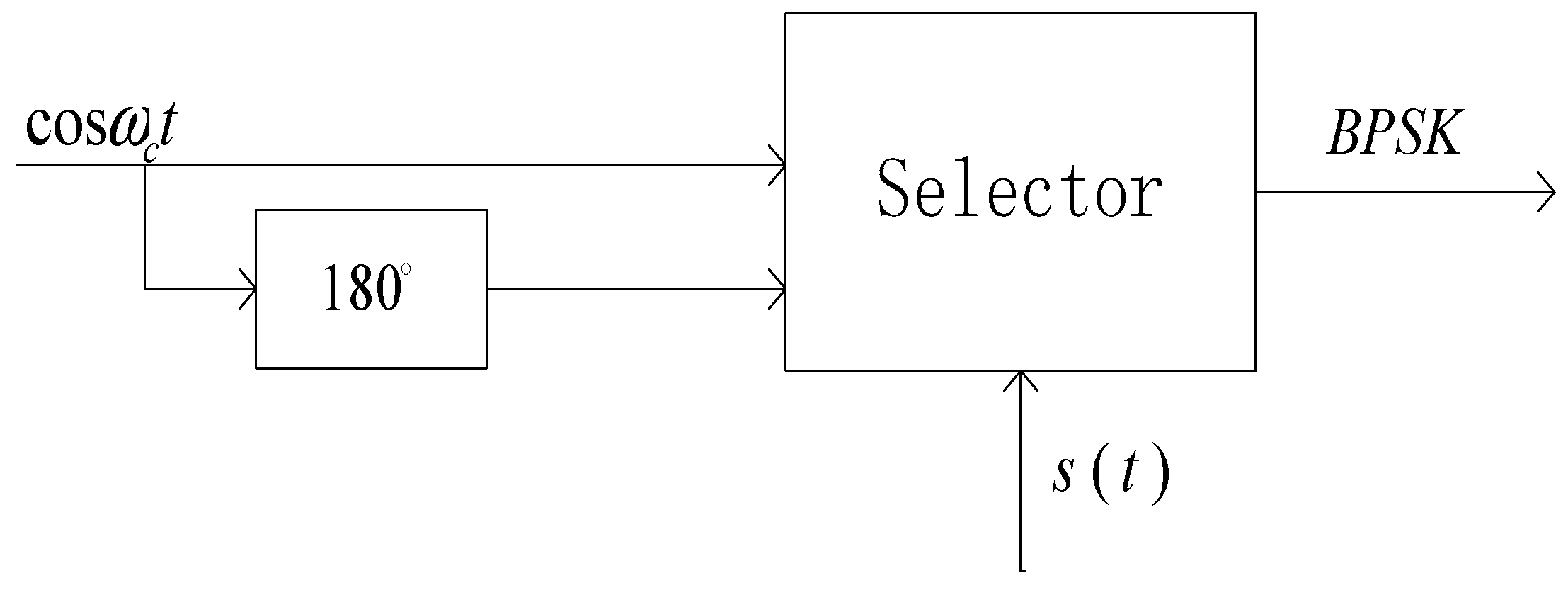
In this paper, as the selection method to generate the BPSK signal we used the baseband signal to control a switching circuit to select the input signal. The input signal of the switching circuit is two co-frequency carriers whose phase difference is
π.
Figure 2 shows the block diagram of our BPSK modulation module:
Figure 2.
Block diagram of Binary Phase Shift Keying (BPSK) modulation.
Figure 2.
Block diagram of Binary Phase Shift Keying (BPSK) modulation.
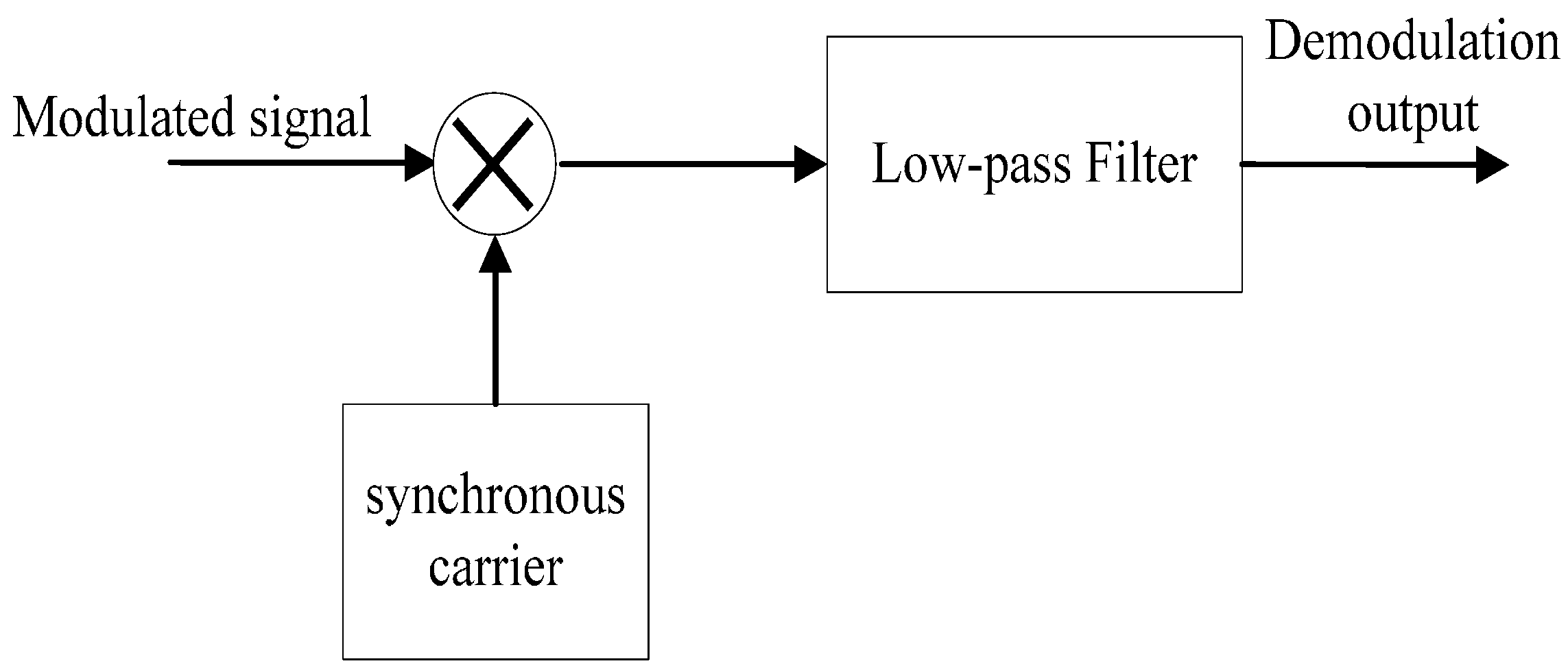
Coherent demodulation and incoherent demodulation are two common demodulation methods. Coherent demodulation has great advantages with regard to threshold detection, output signal to noise ratio, error rate and others, and is the method used in this paper. The block diagram of the BPSK demodulation module is shown in
Figure 3.
Figure 3.
Block diagram of BPSK demodulation.
Figure 3.
Block diagram of BPSK demodulation.
2.3. Carrier Synchronization
The Costas loop synchronization method is used in the carrier synchronization module [
14]. Coatas loop synchronization belongs to the direct methods [
15]. Compared to the pilot carrier method, direct method can extract the carrier from the signals without a pilot signal. Direct methods can achieve carrier synchronization using the modulated signal as an input. Direct methods not only save resources but are also very useful in cases of limited spectrum resources [
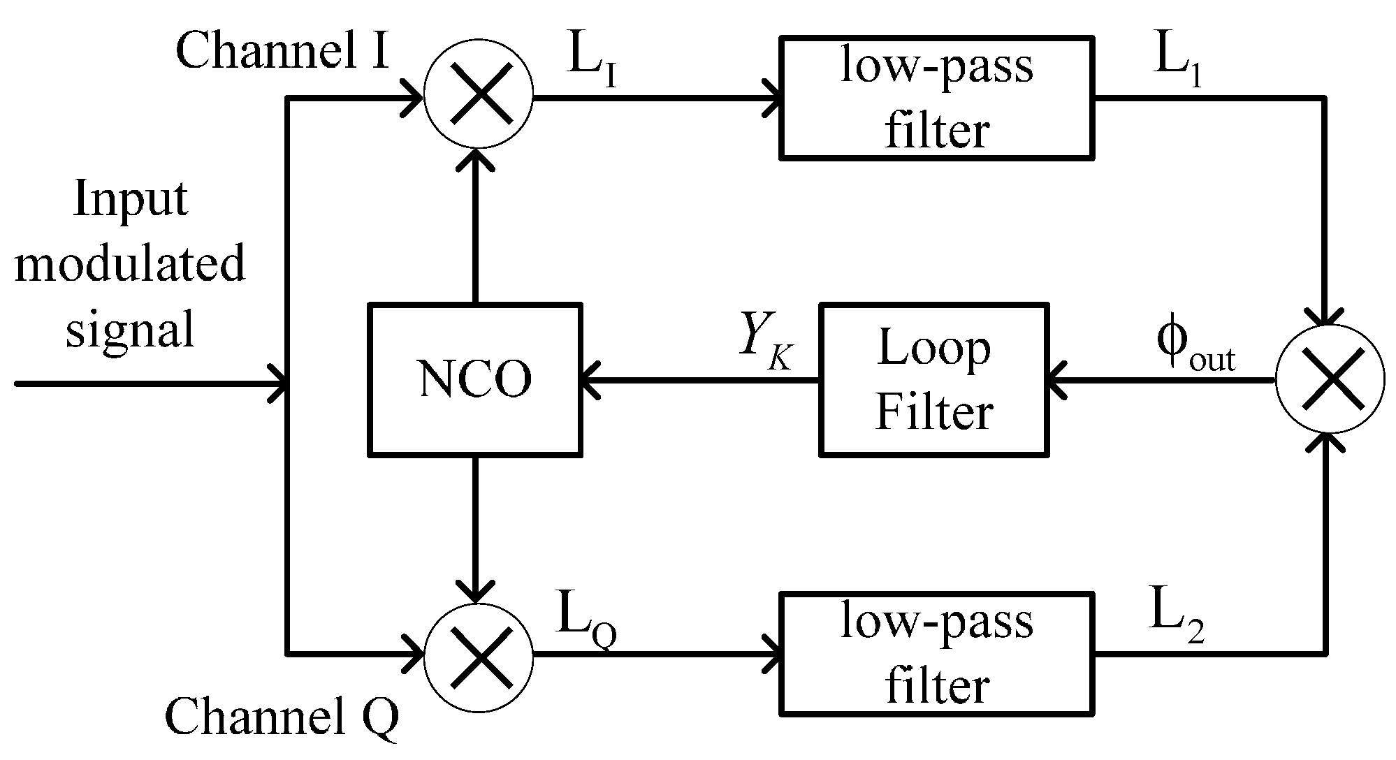
16]. The block diagram of the Costas loop is shown in
Figure 4. The process of the Costas loop can be expressed mathematically as follows:
Figure 4.
Block diagram of the Costas loop.
Figure 4.
Block diagram of the Costas loop.
Let us define the input signal of the Costas loop as
m (
t) cos
ϕt, where
m (
t) denotes the baseband signal, and φ denotes the angular frequency of the carrier of the transmitter. Hence, the signals of the orthorhombic channel I and channel Q can be expressed as Equations (3) and (4), respectively:
The phase difference between the local carrier signal and the input modulated signal is φ. Hence, we obtain Equations (5) and (6).
Equations (7) and (8) are obtained after
LI (
t) and
LQ (
t) go through the low-pass filter:
We then multiply
L1 (
t) by
L2 (
t) to find the error signal, which is expressed by Equation (9):
From the above equations, we see that the local NCO control signal will control the frequency and phase of NCO until the carrier loop is in synchronization [
17]. The carrier signal can then be extracted by tracking the frequency and phase of the transmitter.
3. Code Synchronization Algorithm Based on the Segment Correlation
First, the overall design scheme and block diagram of the code synchronization module are described in this section. Then code acquisition is described in detail, while existing problems of traditional series code acquisition methods are pointed out and corrected, and a novel series code acquisition method based on the segment correlation is implemented. Finally, the code tracking module is described.
3.1. Overall Design of the Code Synchronization Module
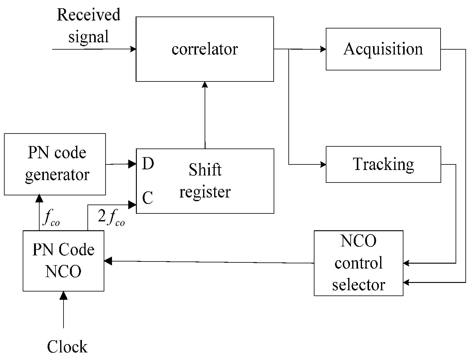
The overall block diagram of the code synchronization module in the digital transceiver is shown in
Figure 5. The workflow of the code synchronization process can be summarized as follows:
- (1)
A correlation operation between the received signal and the carrier signal is applied by the correlator.
- (2)
Then, the computed value is analyzed by the code acquisition module. The phase difference between the carrier signal generated by the local NCO and the carrier signal of the received signal will meet the design requirement after it passes through the code acquisition module.
- (3)
Tracking operation and adjustment will be performed. The phase difference between the local carrier signal and the carrier of the received signal is further decreased during the tracking process by adjusting the clock of the local code generator step by step [
18].
Figure 5.
Block diagram of the code synchronization module.
Figure 5.
Block diagram of the code synchronization module.
The code acquisition module and the code tracking module are the two main components of the code synchronization module. The main work of our paper is to propose a novel code acquisition algorithm.
3.2. Design of the Code Acquisition Module
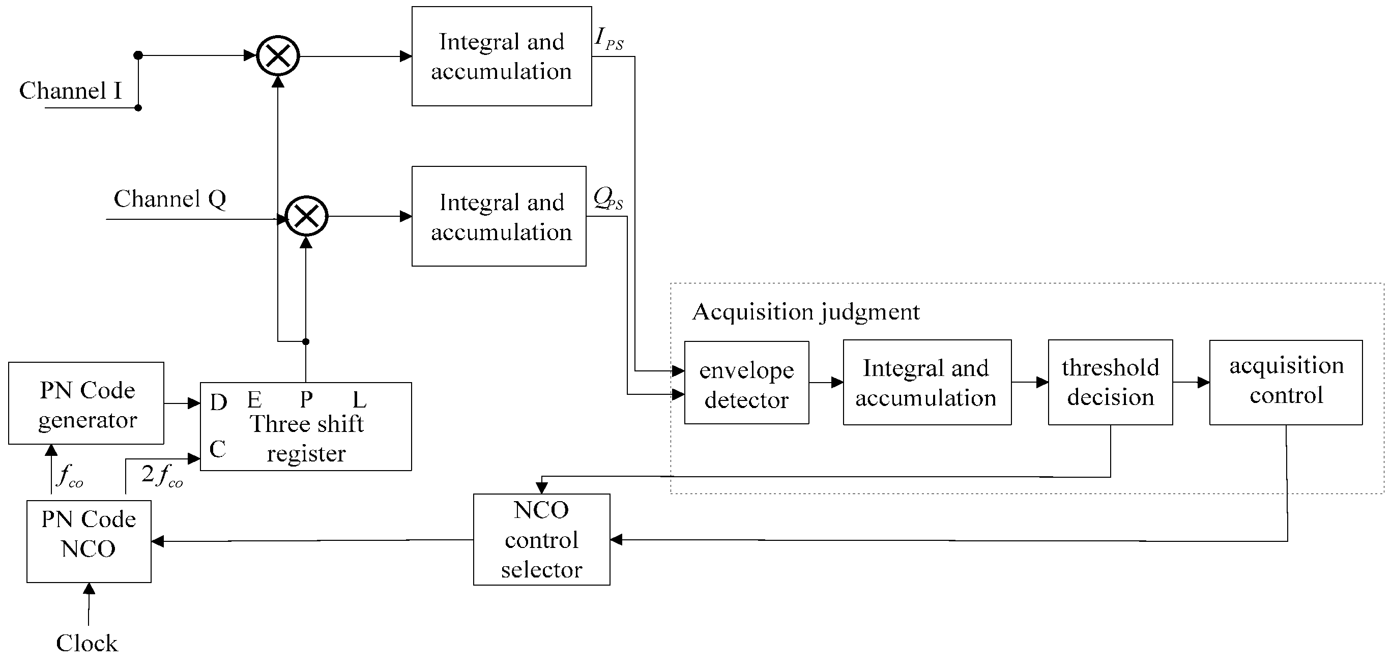
The block diagram of the acquisition loop of the receiver is shown in
Figure 6. The acquisition judgment circuit is the core component of the acquisition loop. The serial acquisition method is used in the acquisition judgment module. The serial acquisition method is well used in situations where the cycle of the carrier signal is short. However, some problems occur when the cycle of the carrier signal is too long. Specific analyses of various such scenarios are described as follows:
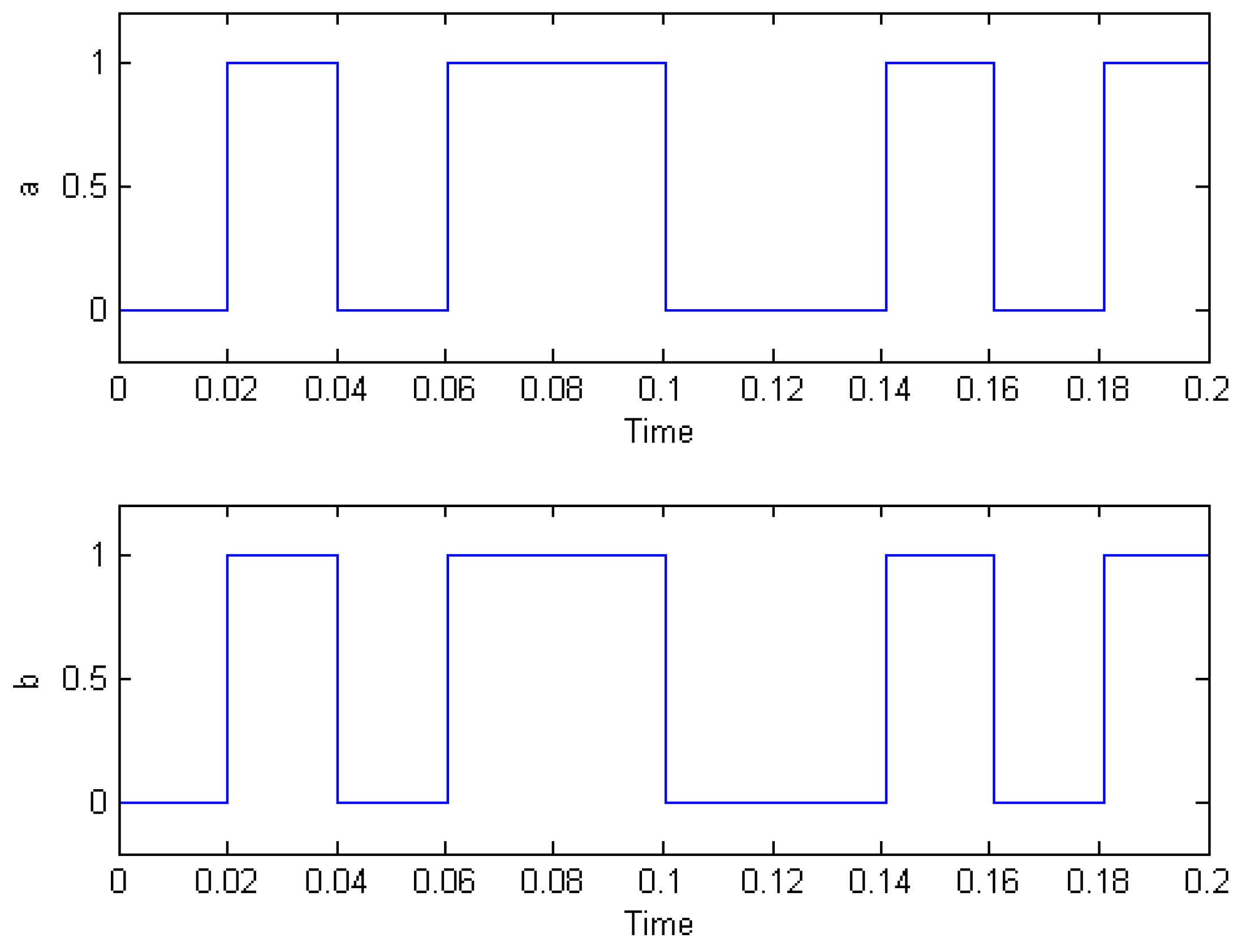
Situation 1: the carrier signal is not inverted after BPSK demodulation. In our case, the word “inverted” means that positive carrier signals before BPSK demodulation turn into negative carrier signals after BPSK demodulation. The signal waveform of such a situation is shown in
Figure 7. After the correlation accumulation operation, the output signal is positive peak-to-peak. Acquisition judgment methods can succeed in such cases,
i.e. carrier signals can be correctly restored after BPSK demodulation.
Figure 6.
The block diagram of the acquisition loop of the receiver.
Figure 6.
The block diagram of the acquisition loop of the receiver.
Figure 7.
Carrier signal example indicative of the first situation.
Figure 7.
Carrier signal example indicative of the first situation.
Figure 8.
Carrier signal example indicative of the second situation.
Figure 8.
Carrier signal example indicative of the second situation.
Figure 9.
Carrier Signal of the third situation.
Figure 9.
Carrier Signal of the third situation.
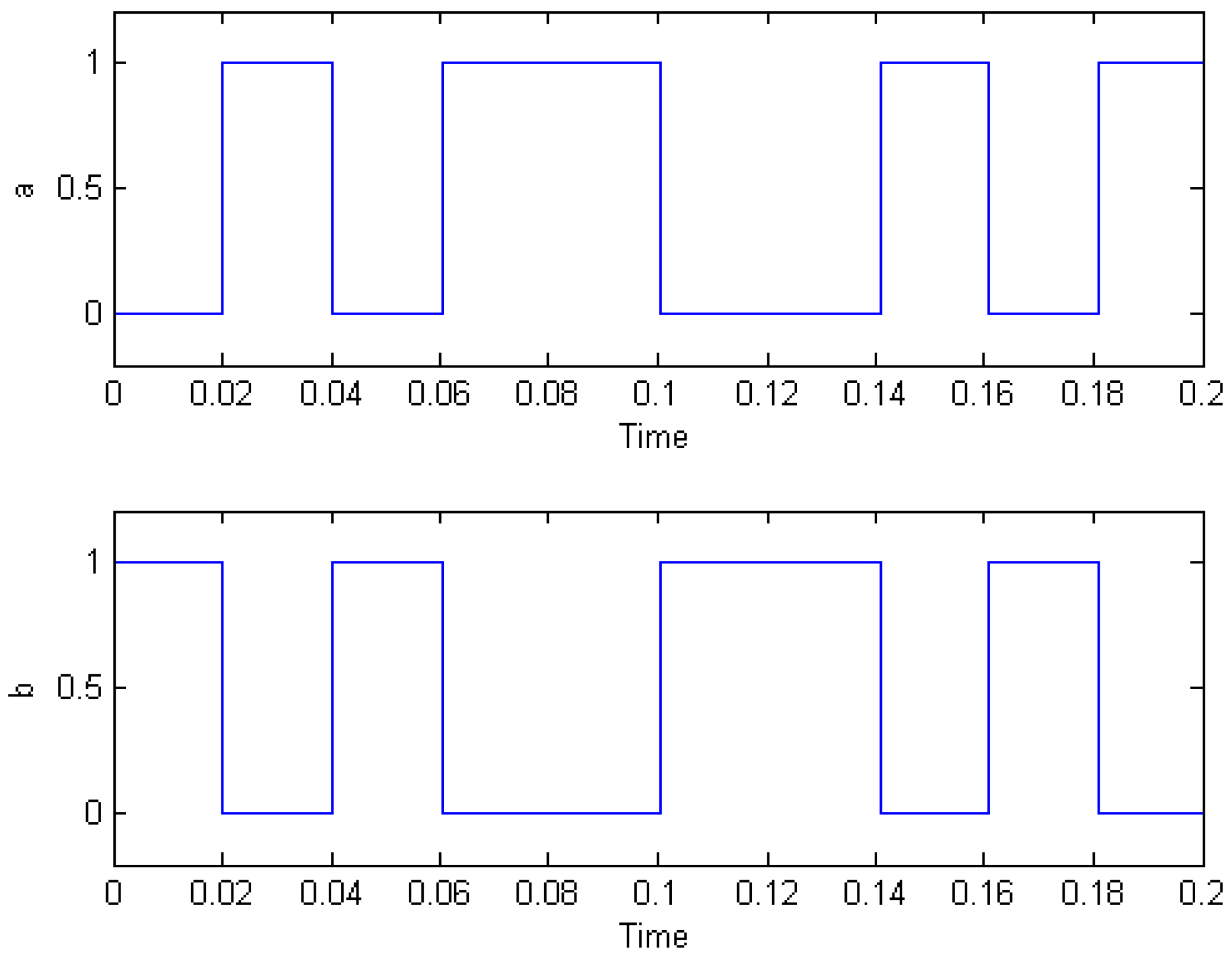
Situation 2: the carrier signal is inverted after BPSK demodulation, while the data acquisition time of the correlative accumulation is reasonable. A sample signal waveform of such a situation is shown in
Figure 8. After the correlation accumulation operation, the output signal is negative peak-to-peak. Acquisition judgments also can succeed in such situations.
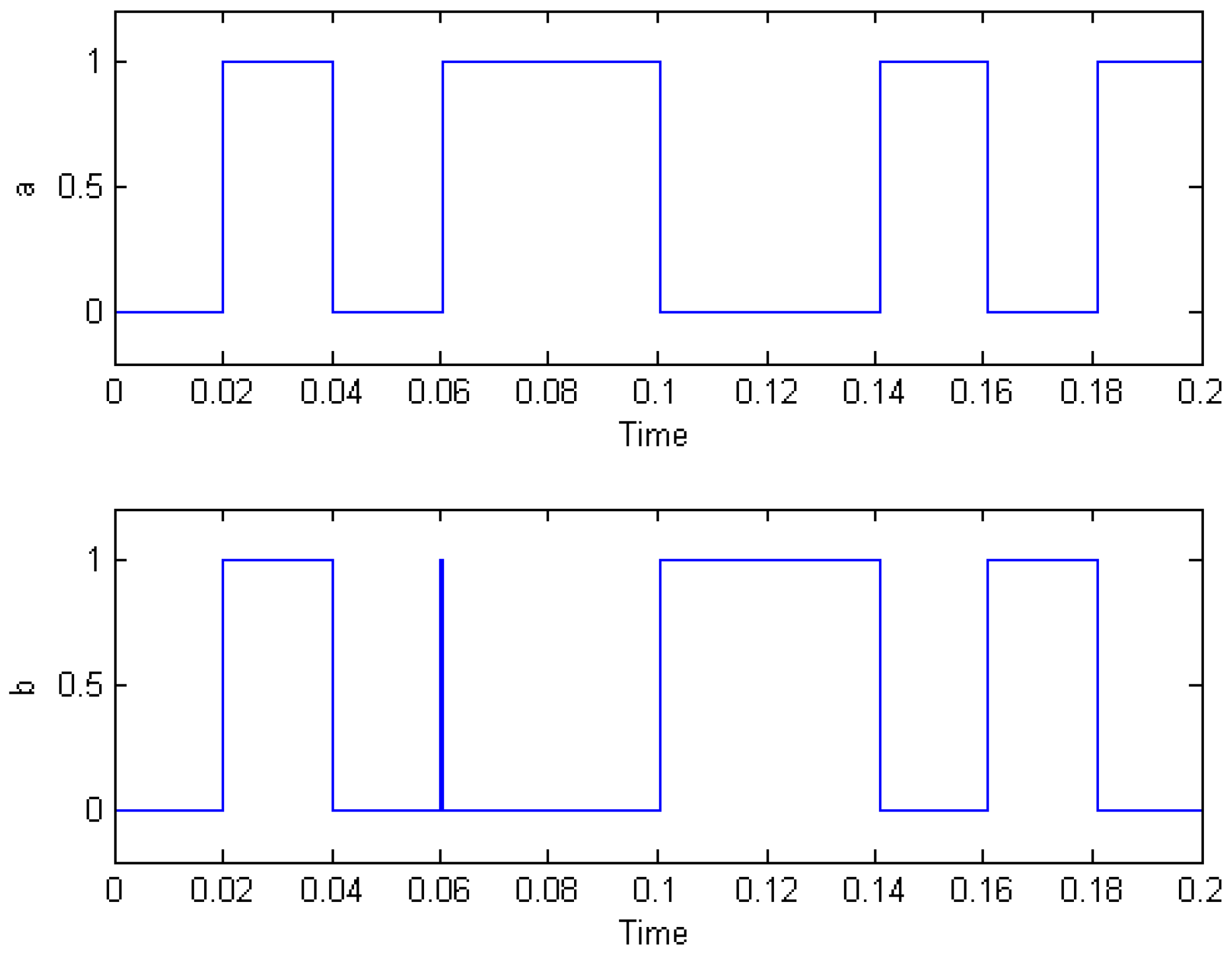
Situation 3: the carrier signal is inverted after BPSK demodulation, but the data acquisition time of the correlative accumulation is not reasonable. This situation is shown in
Figure 9. In this situation, although the signal is acquired, the value after accumulation is far less than the threshold value which we have set and erroneous judgment occurs.
Hence, to avoid unsuccessful acquisitions, a novel serial acquisition algorithm based on segment correlation is proposed.
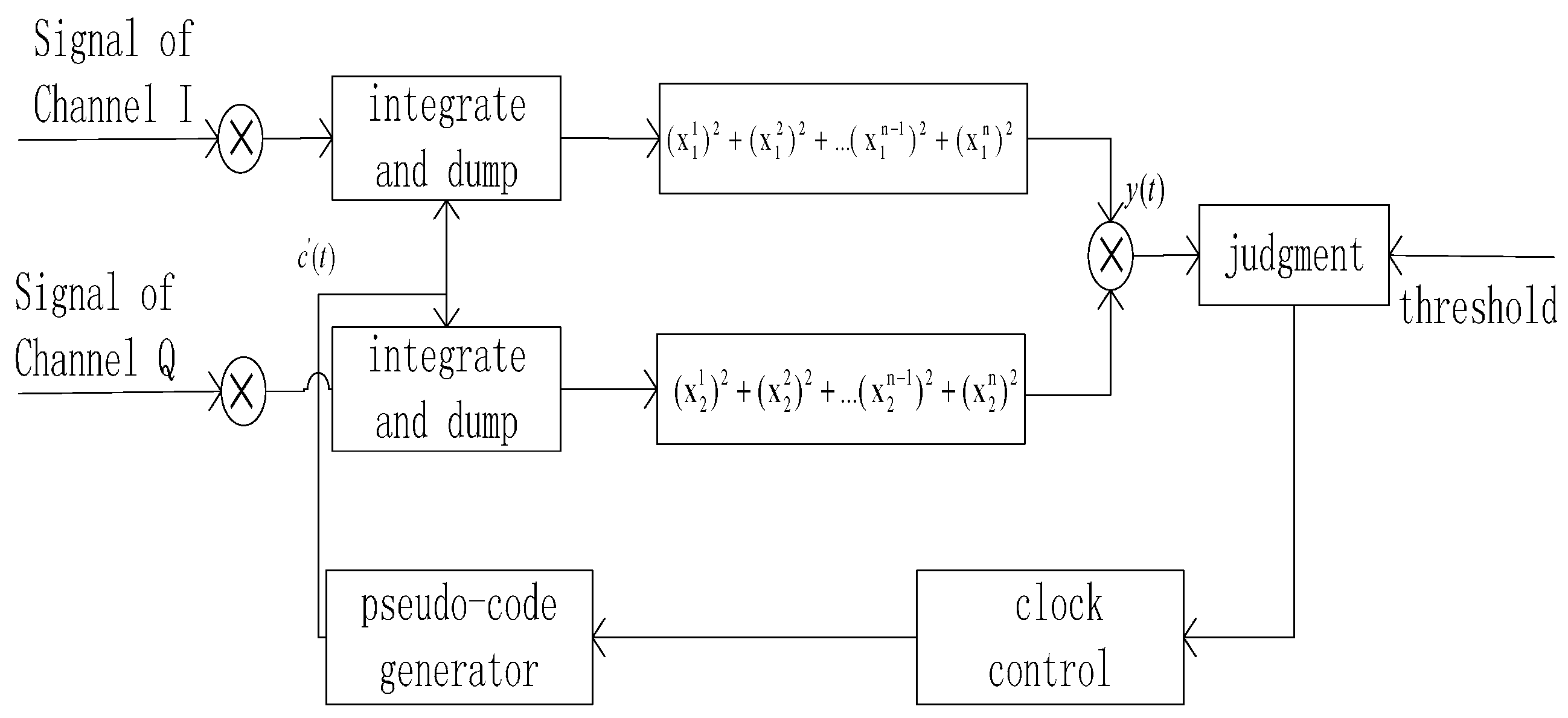
Unlike traditional code acquisition algorithms, our proposed acquisition algorithm is based on correlation that is performed after partitioning each acquisition time interval into smaller segments. Then, a correlation operation is performed between acquisition data for each such segment. After the correlation operation, the absolute values of the obtained correlation operation results of segment are summed. The accumulated value is used as the final code acquisition value of each acquisition time interval. The block diagram of the proposed serial acquisition algorithm is shown in
Figure 10. In the proposed serial acquisition algorithm, the absolute value of the results obtained after the correlation operation are the peak-to-peak values in each time segment. Peak-to-peak values will be acquired by adding the peak-to-peak values in each segment of the acquisition time interval. In this manner, erroneous judgments are avoided and, hence, the capturing efficiency is improved.
Figure 10.
Block diagram of the proposed serial acquisition algorithm.
Figure 10.
Block diagram of the proposed serial acquisition algorithm.
3.3. Code Tracking
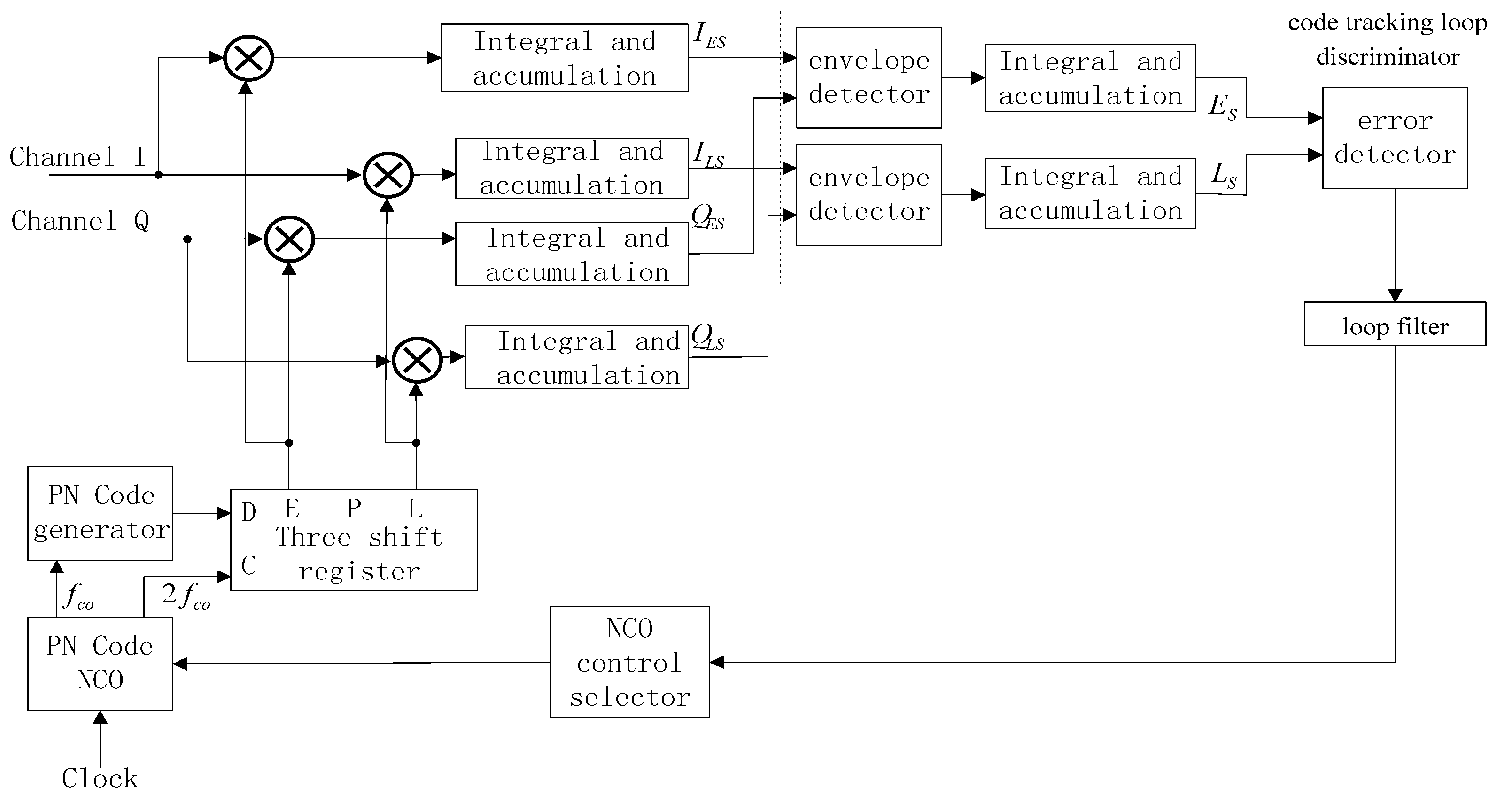
The block diagram of code tracking loop module used in this paper, which is based on a delay-locked loop, is shown in
Figure 11. Its main components are the code tracking loop discriminator and loop filter.
The algorithm of the discriminator can be expressed through Equation 10:
where,
and
.
Figure 11.
Block diagram of code tracking loop module.
Figure 11.
Block diagram of code tracking loop module.
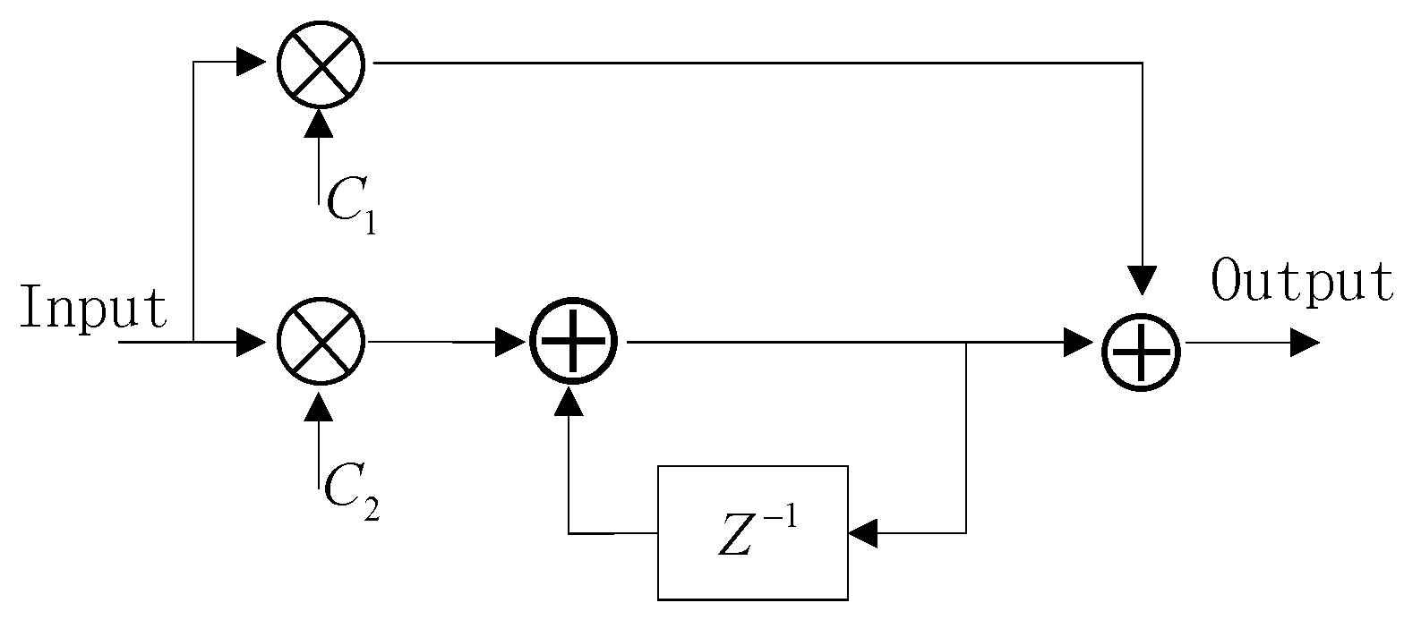
The loop filter plays an important role in the code tracking loop. Compared with a first-order or a third-order loop filter, a second-order loop filter has many advantages, such as: the frequency deviation is constant; the zero-frequency gain is infinite; its stability is very good it is also easy to implement. This paper adopts a second-order loop filter solution, the frequency domain model of which is shown in
Figure 12.
z−1 denotes the unit delay of the integrator.
Figure 12.
The frequency domain model of the second-order digital loop filter.
Figure 12.
The frequency domain model of the second-order digital loop filter.
4. Simulation
In this section, the simulations of the M-sequence, the BPSK modulation, the NCO module, the low-pass filter, the carrier synchronization, and the code synchronization modules of the DSSS transceiver, based on the proposed code synchronization algorithm, are presented, in order to demonstrate the role of each of the different modules and prove the advantages of our approach.
4.1. M-Sequence Module
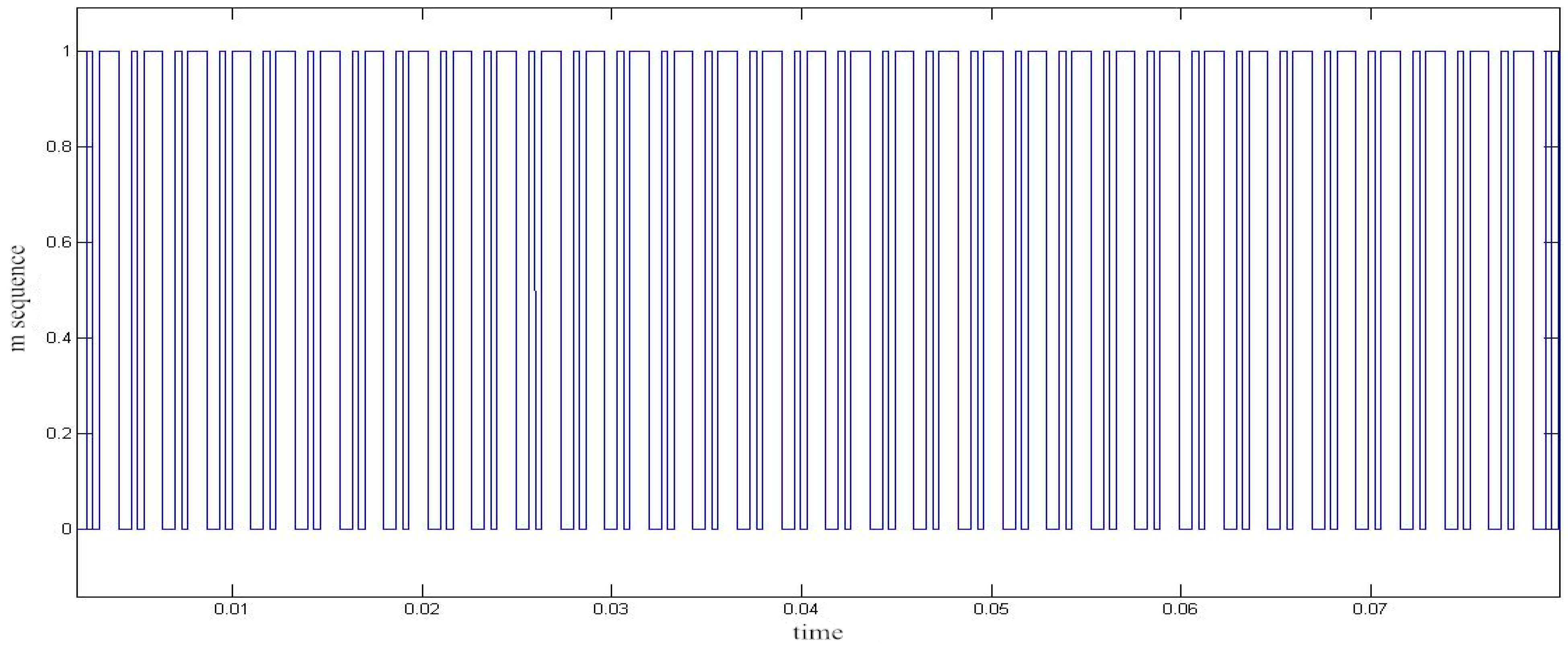
An M-sequence is first generated by a shift register. The Matlab-generated simulation result of the M-sequence module is shown in
Figure 13.
Figure 13.
The simulation result of the M-sequence module.
Figure 13.
The simulation result of the M-sequence module.
4.2. BPSK Modulation
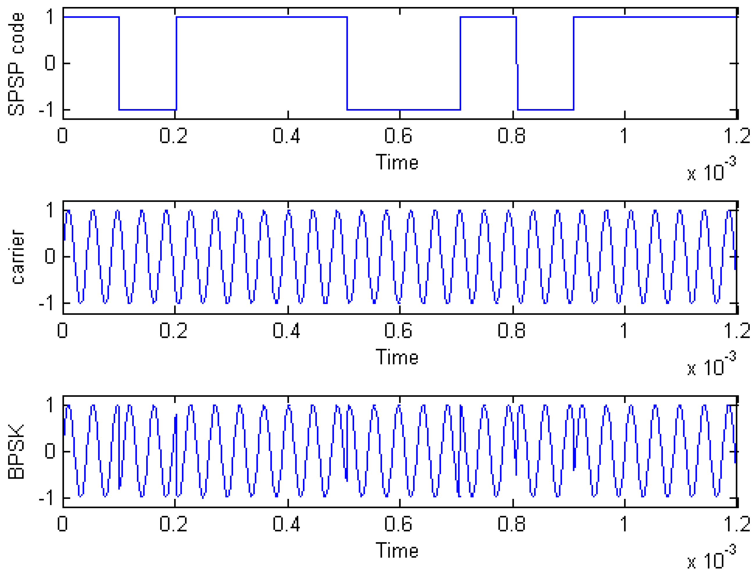
We then multiply a baseband signal by the M-sequence to get SPSP. The simulation result, as obtained using Matlab, is shown in
Figure 14.
The SPSP sequence will be obtained after the baseband signal has been spread. BPSK modulation is then performed by passing the SPSP sequence through a modulator. The simulation result of the BPSK modulation is shown in
Figure 15.
Figure 14.
Simulation result of Spread Spectrum (SPSP).
Figure 14.
Simulation result of Spread Spectrum (SPSP).
Figure 15.
The simulation result of BPSK modulation.
Figure 15.
The simulation result of BPSK modulation.
Figure 16.
Simulation result of demodulated waveform.
Figure 16.
Simulation result of demodulated waveform.
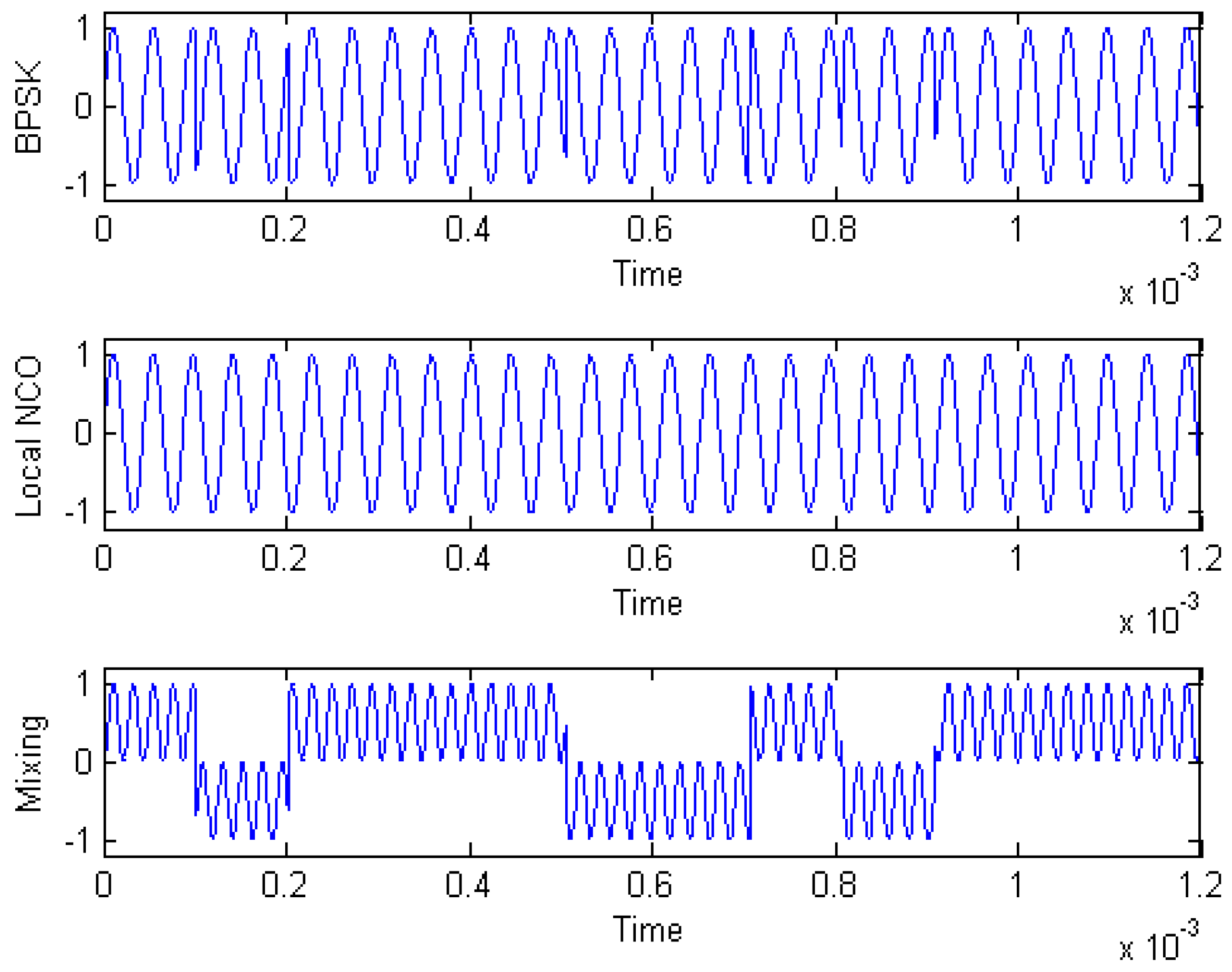
After spreading the spectrum and modulating the baseband signal, we transmit it and demodulate the waveform to verify whether we can recover the original SPSP waveform correctly. The demodulated waveform is shown in
Figure 16, from which we see that the demodulated waveform is as same as our initial one shown in
Figure 14.
4.3. NCO Module
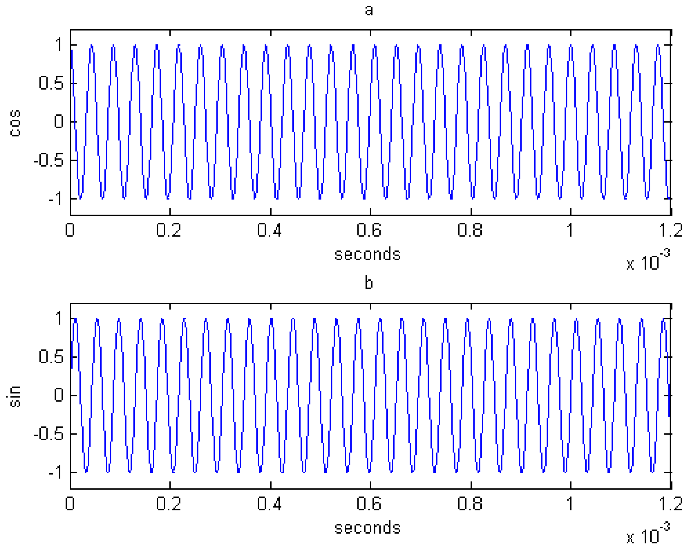
The purpose of the NCO module is to generate two mutually orthogonal signals. The technological basis of NCO is Direct Digital Synthesizer (DDS) technology [
19,
20,
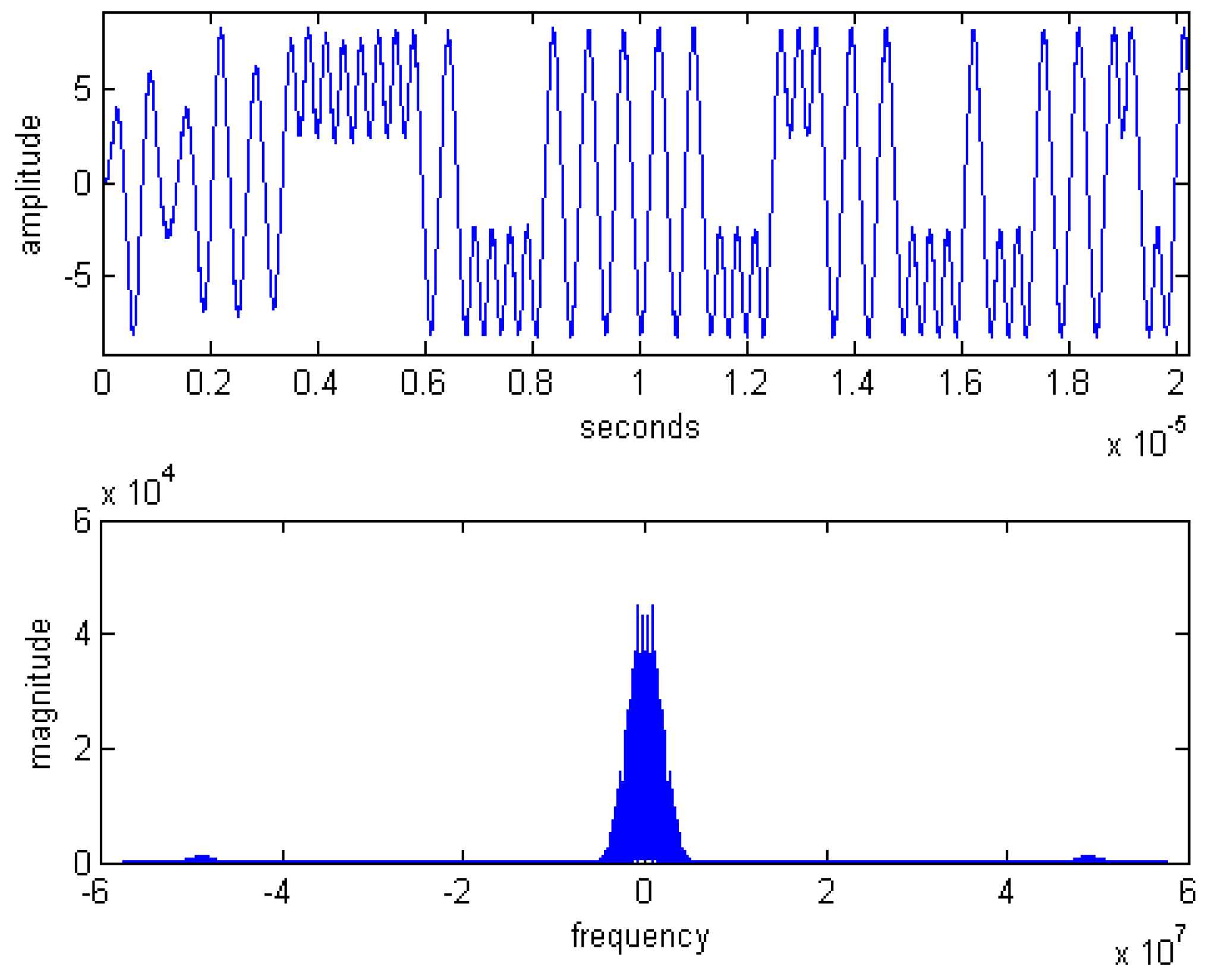
21]. The simulation result of the NCO module output is shown in
Figure 17.
Figure 17.
Simulation result of NCO.
Figure 17.
Simulation result of NCO.
4.4. Low-Pass Filter
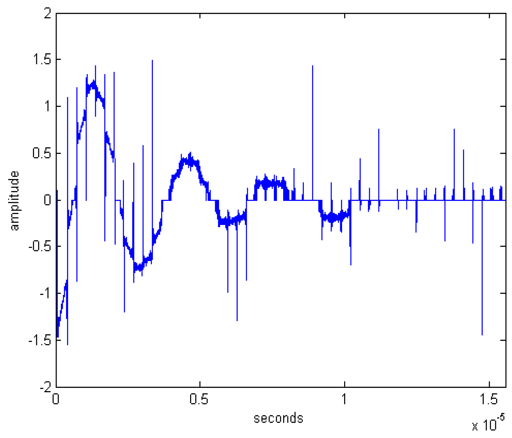
From
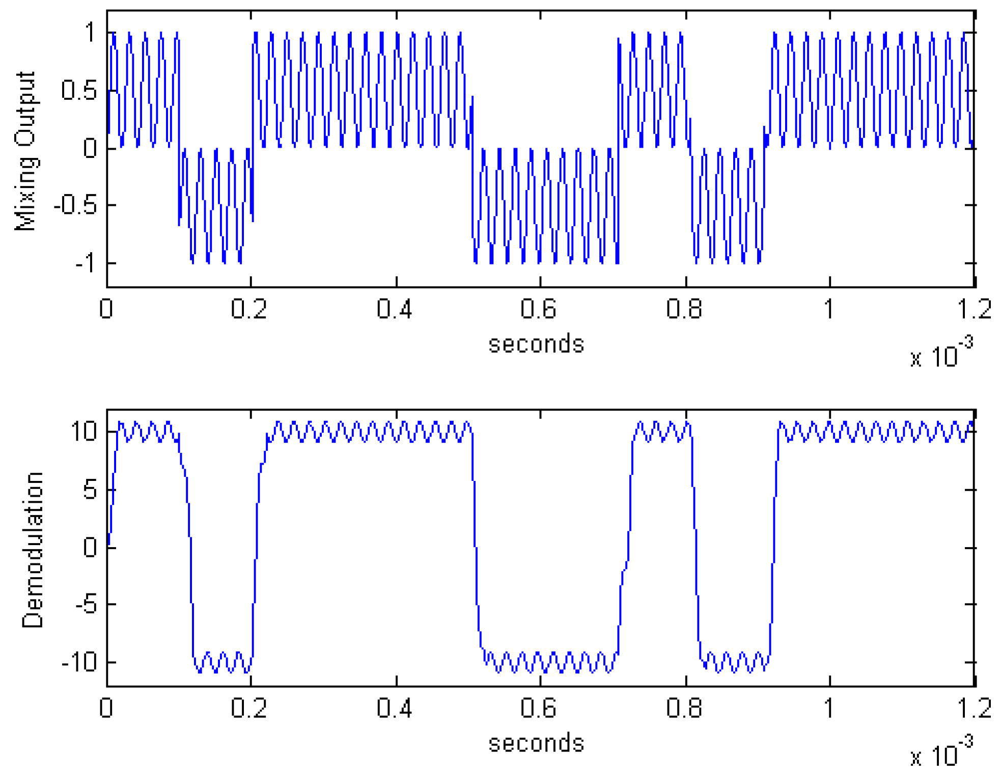
Figure 17, we can see that there are many harmonic components, which do not meet our design requirements. The signals that we want to obtain are zero medium frequency signals. Hence, we need to process the mixed signal effectively, which implies using a low-pass filter. The low-pass filter in this paper is implemented through an integration and accumulation manner. The main function of the low-pass filter is to filter high frequency components. The simulation result of the low-pass filter for the mixing output of
Figure 16 is shown in
Figure 18.
Figure 18.
Simulation result of low-pass filter.
Figure 18.
Simulation result of low-pass filter.
4.5. Carrier Synchronization
The carrier synchronization module used in our system is based on the Costas loop. In this module, the carrier loop phase detector constitutes an important component, as it is used to compare phases [
22]. This paper uses CORDIC algorithm to implement an arc tangent phase detector [
23,
24]. The simulation result of the phase detector is shown in
Figure 19, from which we can see that at the beginning of loop, a phase difference exists, but the output value of the phase detector will tend towards 0 as the carrier approaches synchronization.
Figure 19.
Simulation result of phase detector.
Figure 19.
Simulation result of phase detector.
The simulation result of the carrier loop is shown in
Figure 20. In this figure, we can see that high frequency components have been filtered and that the baseband signal will be obtained after the received signal is demodulated.
Figure 20.
Simulation result of carrier loop.
Figure 20.
Simulation result of carrier loop.
4.6. Code Acquisition
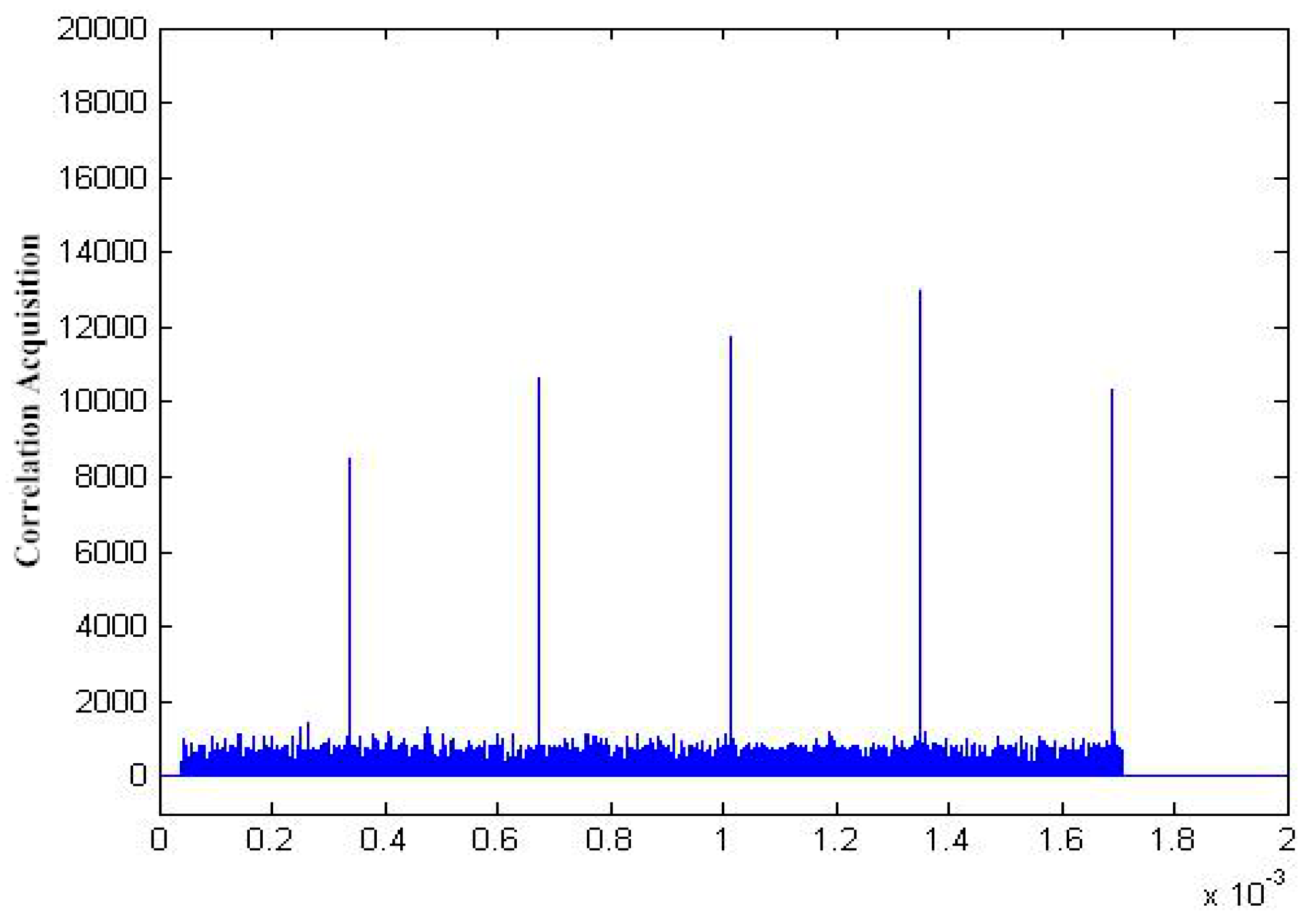
The purpose of the code acquisition simulation is to verify the theoretical feasibility of code acquisition loop. In this simulation, two M-sequences whose phases are different are first generated. These two M-sequences have same cycle. Following the circular method, we slide one M-sequence as a correlative operation is conducted among the points in one fixed cycle during slide process. Then, we sum the values which are the result of the correlative operation. Given the autocorrelation properties of M-sequences, peak values will appear when the phase difference of these two M-sequences meets the code acquisition requirement; otherwise, near-zero values will appear. The simulation result of code acquisition is shown in
Figure 21, which shows peak values when the phase difference between two M-sequences meets the code acquisition requirement. Otherwise, the output values remain at very low levels.
Figure 21.
Simulation result of code acquisition.
Figure 21.
Simulation result of code acquisition.
4.7. Code Tracking
The code acquisition loop provides rough synchronization while the code tracking module gives us subtle synchronization. Code tracking cannot change the timer of the code generator significantly, but does so step by step according to the effect of the phase detector and the loop filter to achieve the end goal [
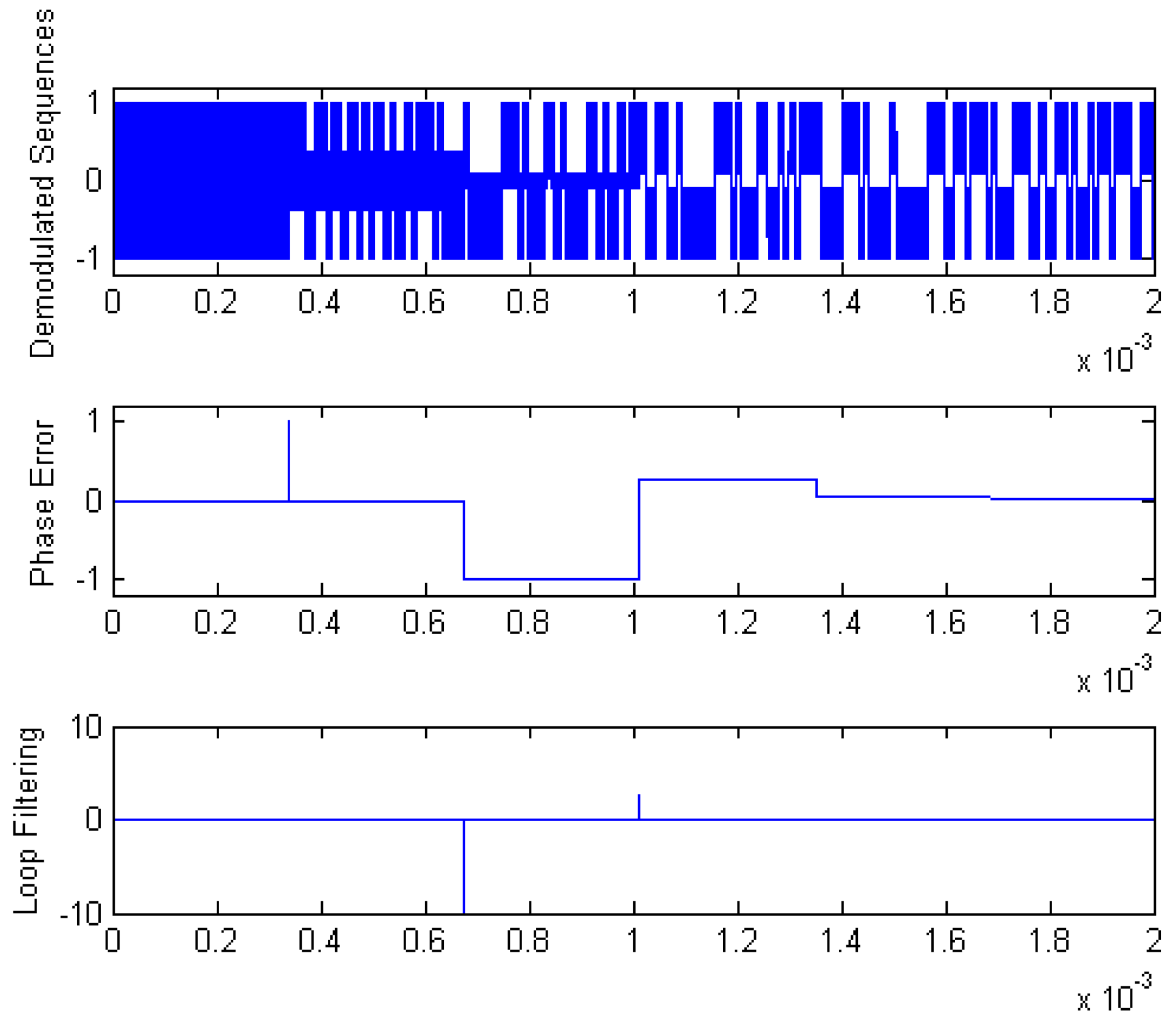
25]. The simulation result of the code tracking module is shown in
Figure 22.
From
Figure 22, we can see that the phase difference decreases with successive loop iterations and slowly converges to zero, which illustrates that the phase difference between two sequences are decreasing step-wise. The output of the loop filter changes with the output of phase difference. Besides, we can see that the output of loop filter is comparatively high when the phase difference is comparative big, which leads to the significant adjustment of the overall loop. Accordingly, the output of the loop filter is comparatively small when the phase difference small, and is equal to zero when there is no phase difference.
Figure 22.
Simulation result of code tracking.
Figure 22.
Simulation result of code tracking.
4.8. Code Synchronization
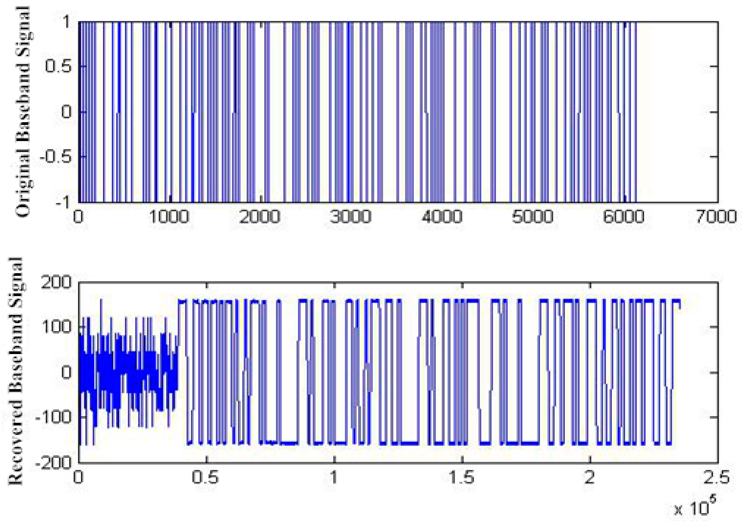
The simulation of overall code synchronization combines code acquisition and code tracking, demodulation of the modulated baseband signal through code synchronization, and restoration of the baseband signal. The simulation result of overall code synchronization is shown in
Figure 23, which shows that the demodulated baseband signal is chaotic when the signal is not synchronized and correctly restored when the signal is synchronized. Hence, we see that the DSSS receiver restores the signals transmitted by the transmitter accurately with regard to both time and frequency, based on our proposed serial code acquisition.
Figure 23.
Simulation of code synchronization.
Figure 23.
Simulation of code synchronization.
5. FPGA Implementation
The PCB design and manufacturing of the hardware platform of the proposed DSSS software transceiver are described in this section. The specific FPGA implementation of the carrier synchronization module, the code acquisition module, the code tracking module are also presented here, along with the implementation of the transmitter and receiver. The full software-based DSSS transceiver design was thus hardware tested on this platform, and its correctness and feasibility were verified through the demonstration of a communications’ channel between two PCs.
5.1. PCB Design and Manufacture of the DSSS Transceiver System
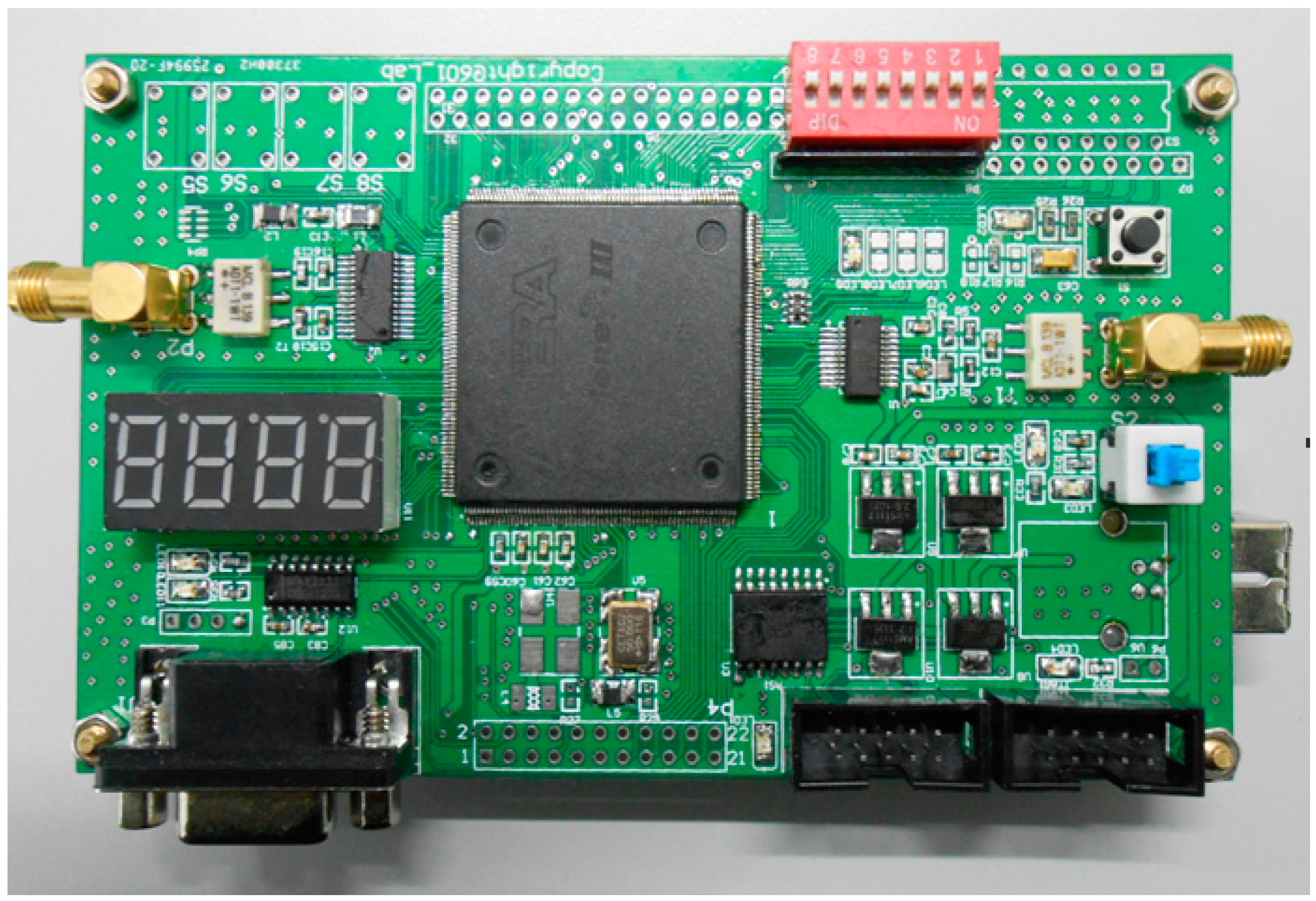
Altium Designer software was used to design PCB in this paper. The main circuits of the DSSS transceiver consist of the following: FPGA core, clock, power, reset, A/D and D/A. A schematic was designed based on these circuits, and then converted to a PCB diagram. Our PCB design uses a double-layer structure and can meet high speed requirements. In addition, it was designed for the maximal suppression of electromagnetic compatibility and crosstalk. Finally, the designed PCB board is welded. The Physical map of the hardware platform is shown in
Figure 24.
Figure 24.
The Physical map of the hardware platform.
Figure 24.
The Physical map of the hardware platform.
5.2. FPGA Implementation of the Carrier Synchronization Module
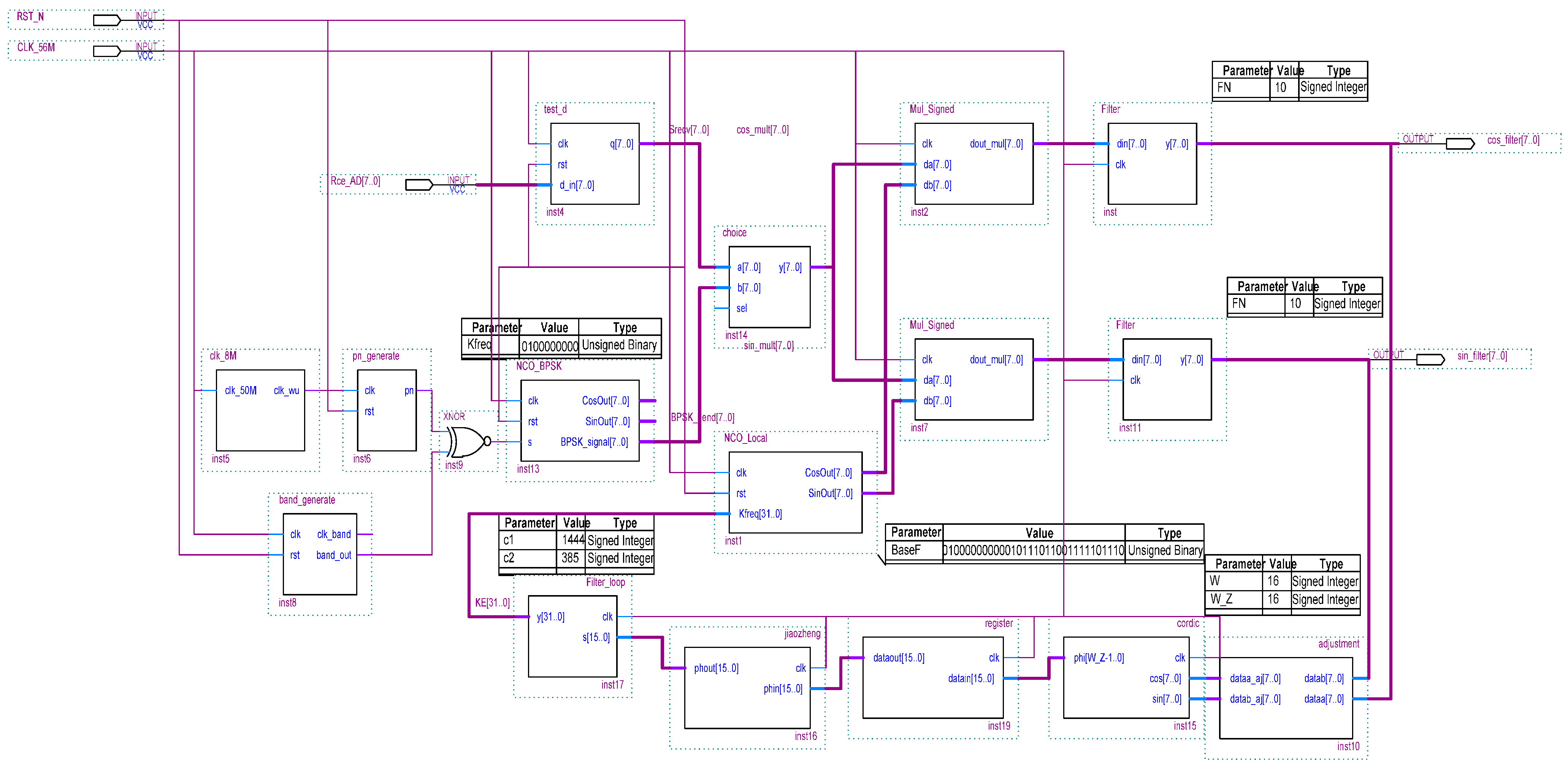
The filter, module, phase discrimination, integral accumulation and NCO modules are the main modules of the carrier loop in our FPGA implementation. The overall FPGA framework of the carrier synchronization module is shown in
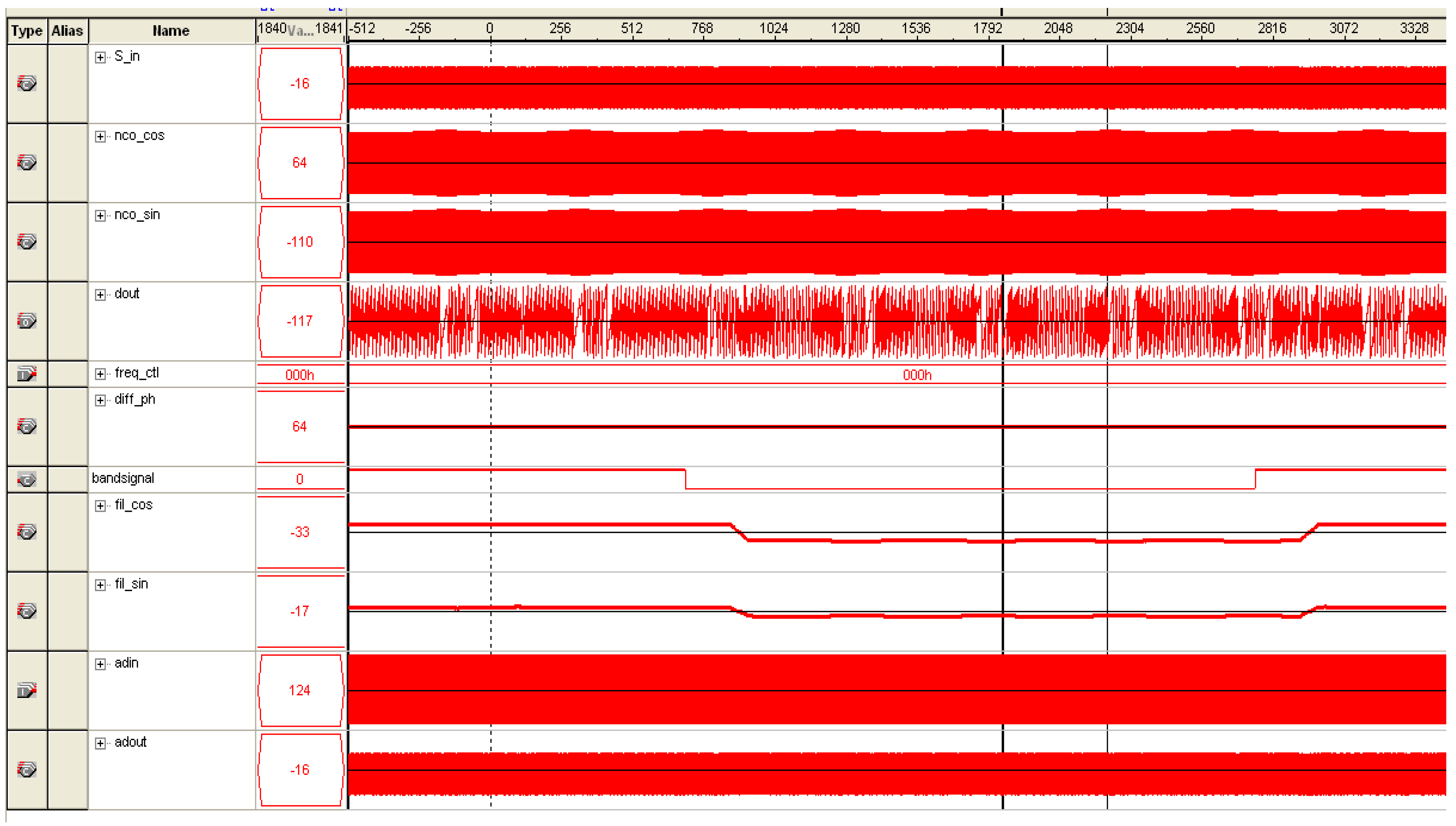
Figure 25. After integrating and adjusting the above modules, we used the logic analyzer of Quartus II for debugging. The signal waveform obtained from the logic analyzer is shown in
Figure 26. From fil_cos and fil_sin in
Figure 26, we see that the baseband signal has been restored, which shows that the FPGA implementation of the carrier synchronization module was for the most part successful.
Figure 25.
The overall FPGA framework of the carrier synchronization module.
Figure 25.
The overall FPGA framework of the carrier synchronization module.
Figure 26.
The waveform of carrier loop synchronization.
Figure 26.
The waveform of carrier loop synchronization.
5.3. FPGA Implementation of the Code Acquisition Module
The FPGA implementation of the code acquisition module is shown in
Figure 27. The module consists of the correlator, operation and judgment modules. The yihuo_mult module in
Figure 27 is the correlator module. The main function of correlator module is to multiply local PN code by received signal. The integer_capture module in
Figure 27 is the operation module. The functions of the operation module are summarized as follows:
- (1)
Segmental integration of the output values of the correlator module.
- (2)
Acquisition of the absolute values of the segmental integrated values.
- (3)
Summation of all the absolute values in one cycle.
- (4)
Threshold judgment of the final added values to judge whether the k and the s signal have been acquired.
Judge module in
Figure 27 is the judgment module. The main function of the judgment module is to judge whether the code acquisition is successful given the values of the k and s signals. G_out = 1 when the code acquisition is successful, in which case the code tracking loop can be initialized.
Figure 27.
The top-level design of the code acquisition module.
Figure 27.
The top-level design of the code acquisition module.
After creating the FPGA code of the code acquisition module, a timing simulation of the programmed FPGA circuit was conducted. The simulation result is shown in
Figure 28. The m_out signal in
Figure 28 is the local PN sequence. m_out3 is the simulative received PN code sequences. k is the flag of unsuccessful acquisition. s is the flag of successful acquisition. When m_out and m_out3 are show that acquisition has been unsuccessful, the output of k is a high level signal while the output of s is a low level signal after one computing cycle. When m_out and m_out3 are acquired in phase, the output of k is a low level signal while the output of s is a high level signal after one computing cycle. These results confirm the proper function of our FPGA design for the code acquisition module.
Figure 28.
Timing simulation of the code acquisition module.
Figure 28.
Timing simulation of the code acquisition module.
After the timing simulation, the code acquisition module was debugged with the use of SignalTap II. The debugging result is shown in
Figure 29. m2 is the local PN code signal generated by the receiver. cos_out is the received PN code signal. G_out16 is the successful flag of code acquisition. From
Figure 29, we can see that the output of G_out16 is at the high level when the phase difference between the local PN code signal and the received PN code signal is less than the minimum chip width.
Figure 29.
The waveform of the code acquisition module.
Figure 29.
The waveform of the code acquisition module.
From the figure, we also see that the proposed improved code acquisition loop system implements the function of the code acquisition module successfully.
5.4. FPGA Implementation of the Code Tracking Module
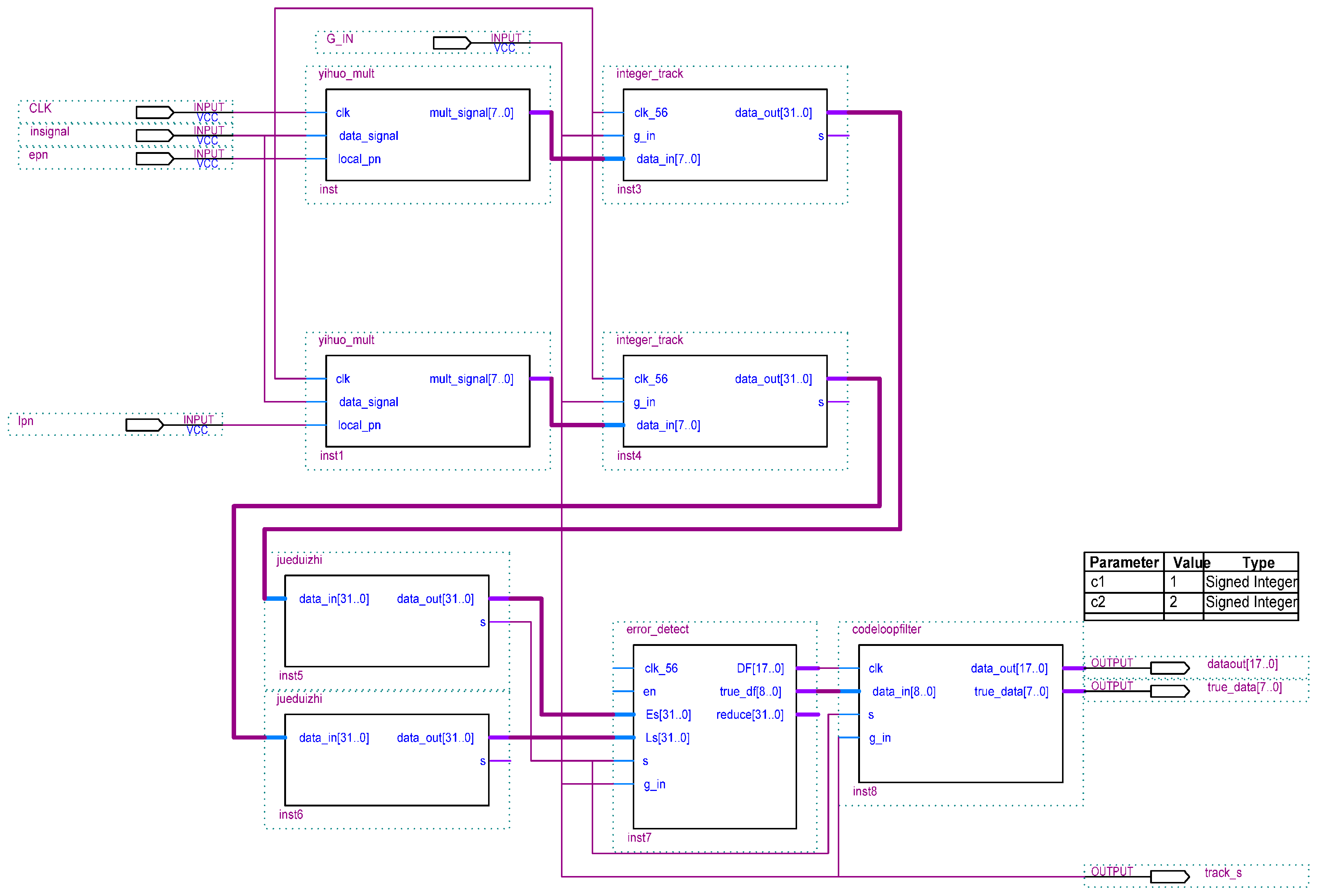
The FPGA module of the code tracking loop is shown in
Figure 30. The main code tracking loop contains the module for the absolute value operation, along with the correlator, integrator, error detector and the loop filter modules. yihuo_mult in
Figure 30 is the correlator module, integer_track is the integrator module, jueduizhi is the operation module for obtaining the absolute values, while error_detect is the error detection module. The main function of the error detector module is to calculate the corresponding phase difference according to the correlation cumulative sum of the anticipated code and lag code between received code and local PN code. In addition, codeloopfilter in
Figure 30 is the loop filter module. The function of this module is to control and adjust the clock of the local PN code generator according to the output error value of the error detection module.
Figure 30.
The top-level design of the code tracking module.
Figure 30.
The top-level design of the code tracking module.
After Verilog coding, a timing simulation of the code tracking module was conducted, the results of which are shown in
Figure 31. m1 and m2 are two PN code signals which have different phase. DF is the output value of the loop filter. Code tracking is successful when the error of the phase difference between the two signal channels is very small. At that moment, the output value of the loop filter is zero.
The result of the system debugging of the code tracking module is shown in
Figure 32. filter_out is the synchronized version of the received signal. cos_out signal is the adjusted filter_out signal, while m2 is the local PN code signal. filter_loop signal is the output value of the loop filter. From
Figure 32, we can see that the output of the loop filter is zero when the local PN code signal tracks the received PN code signal, which verifies the design of the code tracking module.
In summary, the code synchronization system meets the requirements of the digital transceiver.
Figure 31.
Timing simulation result of the code tracking module.
Figure 31.
Timing simulation result of the code tracking module.
Figure 32.
The waveform of the code tracking module.
Figure 32.
The waveform of the code tracking module.
5.5. FPGA Implementation of Transmitter
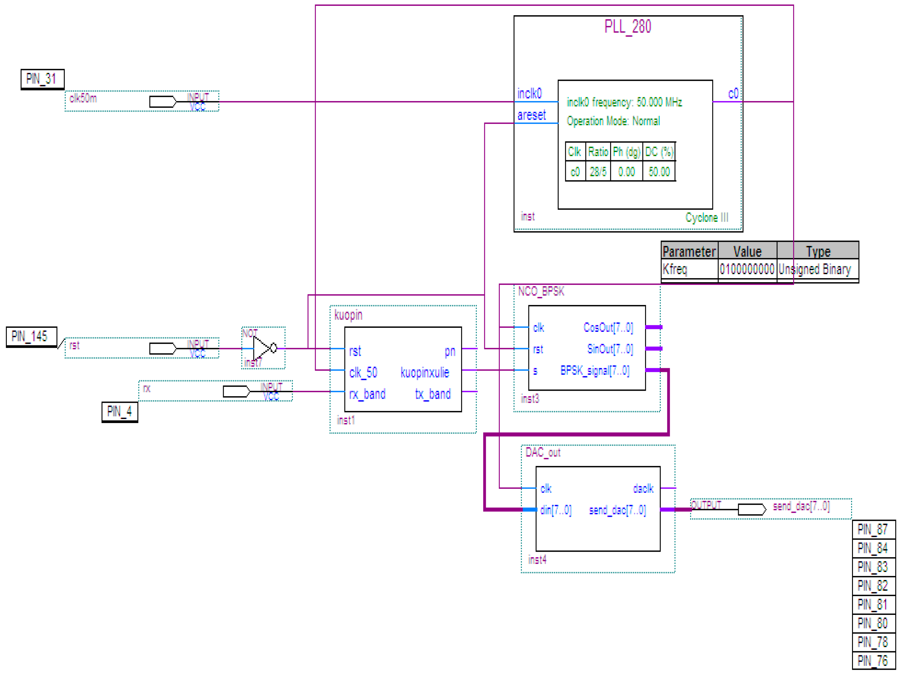
The top-level FPGA design of the DSSS transmitter is shown in
Figure 33. It mainly contains four modules, which are PLL 280, kuopin, NCO BPSK and DAC out. PLL 280 is the SPSP module and is implemented by the SPSP function of Quartus II. The main function of PLL 280 is to generate a systematic clock according to the real system’s requirements. kuopin is the BPSK SPSP module. The main function of kuopin is to make the baseband signal correlate with the local PN code, and then obtain the necessary SPSP code. NCO BPSK is the modulation module, the main function of which is to complete BPSK demodulation. DAC out is the driver module of D/A. The main function of DAC out is to send the modulated digital signal to the D/A converter.
Figure 33.
The top-level design of the Direct Sequence Spread Spectrum (DSSS) transmitter.
Figure 33.
The top-level design of the Direct Sequence Spread Spectrum (DSSS) transmitter.
5.6. FPGA Implementation of Receiver
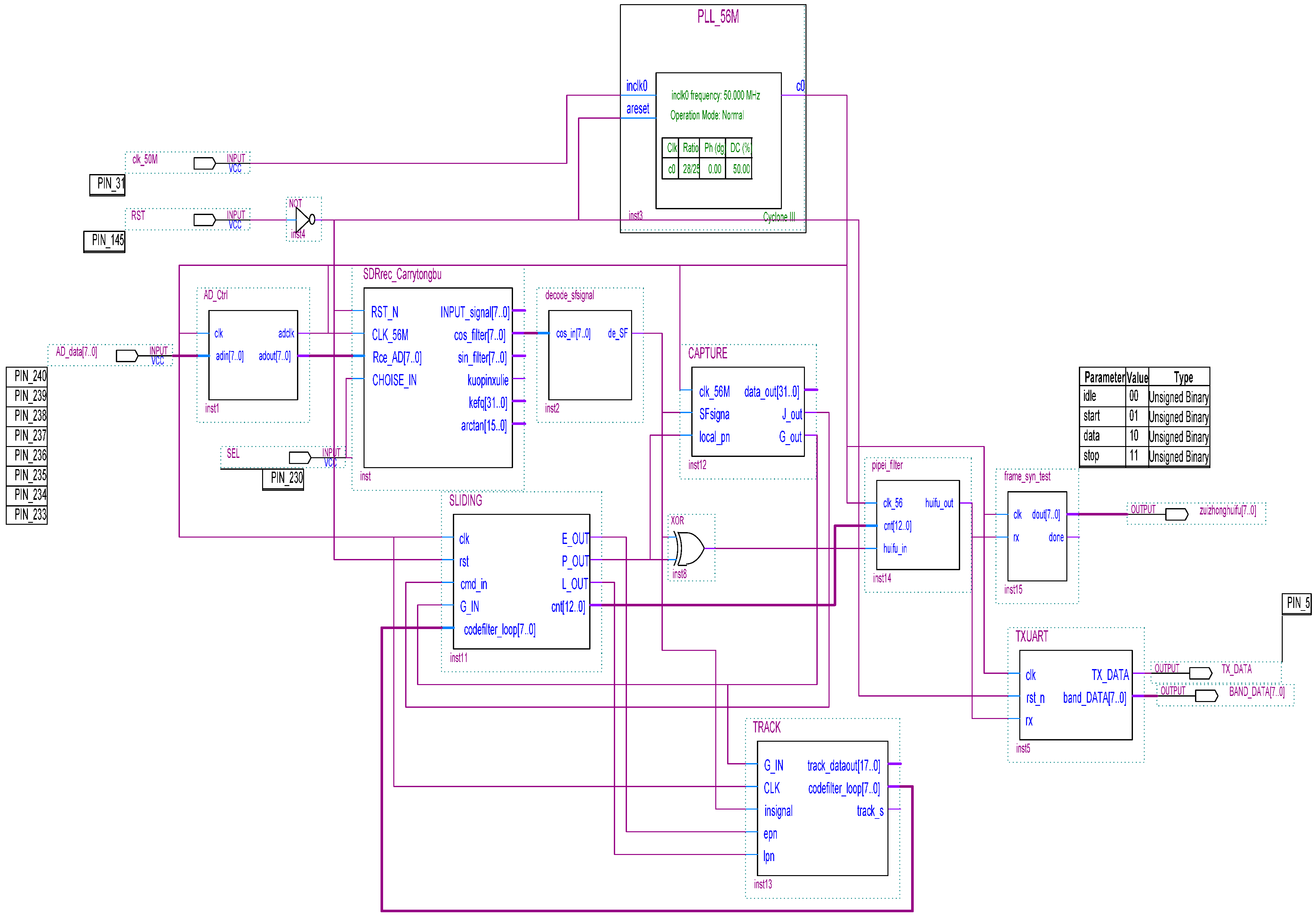
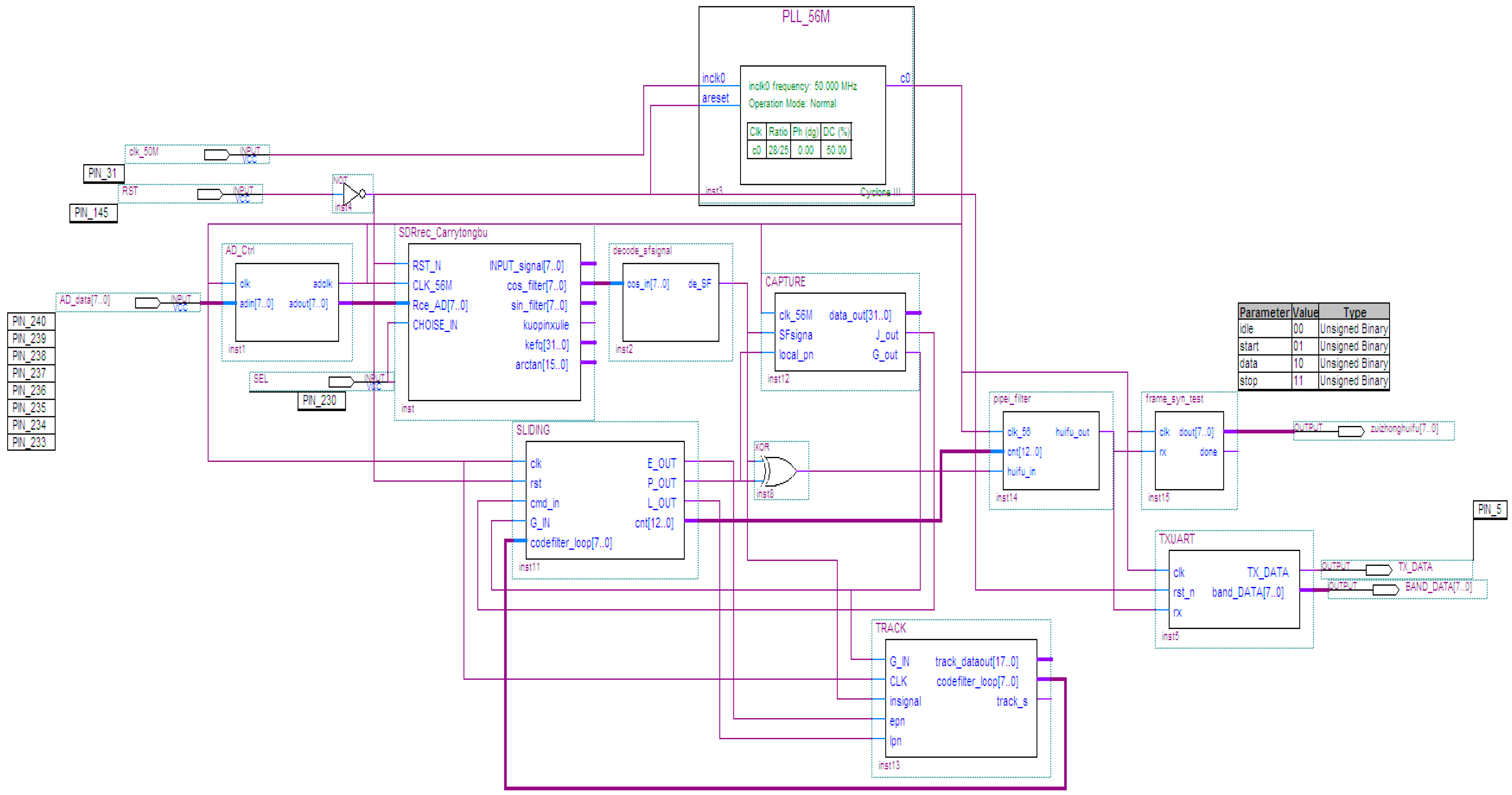
The receiver system is to implement the carrier synchronization loop and the code synchronization loop. The FPGA top-level design of the DSSS receiver is shown in
Figure 34. From this figure, we can see that FPGA receiver contains AD Ctrl, SDRrec Carrytongbu, Capture, Track and Txuart.
Figure 34.
The top-level design of DSSS receiver.
Figure 34.
The top-level design of DSSS receiver.
AD Ctrl is the driver module of the A/D chip. The main function of AD Ctrl is to control the A/D chip, transform the received analog signal into a digital signal, and then load the digital signal to the FPGA. SDRrec Carrytongbu is the carrier synchronization module. Its main function is to load the programmed carrier codes to the FPGA platform. CAPTURE and TRACK are the code acquisition module and code tracking module, respectively. The function of CAPTURE and TRACK are to load the programmed code synchronization module to the FPGA platform. TXUART is the serial port driver module and its function is to transmit the restored original baseband signal to the PC through the serial port. The transmitted information can then be analyzed using PC software.
5.7. Overall Experiment and Demonstration of DSSS Transceiver
First, the DSSS transmitter and receiver are linked by coaxial-cable. Then, the DSSS transmitter and receiver are each linked with a PC using a serial port line. Using Com Wizard, the PC supplies information to the digital transmitter; this information is transmitted to the digital receiver after SPSP and modulation. Then, the signal captured by the digital receiver is restored through demodulation, carrier synchronization and code synchronization. The restored signal is transmitted to the PC, which is linked with the digital receiver. Hence, we can verify whether the original information is restored from receiver PC. The test setup of the DSSS transceiver is shown in
Figure 35, from which we see that the software transceiver is working normally. The signal transmitted form digital transmitter was correctly restored by the digital receiver. The above tests are sufficient to demonstrate the correctness of the designed DSSS software transceiver and the reliability of the proposed code synchronization algorithm.
Figure 35.
The test setup of the DSSS transceiver.
Figure 35.
The test setup of the DSSS transceiver.
6. Conclusions
In this paper, a serial code acquisition method based on segment correlation is proposed. The proposed code synchronization algorithm can deal with misjudgment caused by the unreasonable data acquisition time effectively. An overall communication system based on the proposed code synchronization algorithm is presented. The M-sequence, BPSK modulation and demodulation, NCO, low-pass filter, carrier synchronization and code synchronization modules were simulated using Matlab. Simulation results show the feasibility of the DSSS transceiver based on the proposed code synchronization algorithm. Each module was then coded and debugged using Verilog. Then, the relevant code was loaded on a FPGA system to verify the overall function of the DSSS transceiver. Finally, a PCB board was designed to verify the overall design.
Acknowledgments
The work is supported by Qing Lan Project and the National Natural Science Foundation of China under Grant 61572172 and 61401147 and Natural Science Foundation of Jiangsu Province of China, No.BK20131137 and No.BK20140248.
Author Contributions
Aohan Li proposed the algorithm and prepared the manuscript. Ziheng Yang was in charge of the overall research. Renji Qi and Feng Zhou were in charge of the implementation of the algorithm. Guangjie Han was in charge of drafted and approved the manuscript.
Conflicts of Interest
The authors declare no conflict of interest.
References
- Zhou, X.; Li, J.; Gou, Y. Software radio technology in spread spectrum communications. In Proceedings of the International Conference on Communication Technology Proceedings, Beijing, China, 21–25 August 2000; pp. 1117–1120.
- Lin, J.; Wang, H.; Fang, W.; Liu, Y. The research status survey of software radio. Comput. Meas. Control 2011, 19, 2332–2334. [Google Scholar]
- Jiang, L. Software Radio System Research of PCI Bus. Master’s Thesis, Nanjing University of Aeronautics and Astronautics, Nanjing, China, 2009. [Google Scholar]
- Ma, J. Research and Implementation of GMSK Modulation and Demodulation in Software Radio. Master’s Thesis, Dalian Maritime University, Dalian, China, 2010. [Google Scholar]
- Ma, L. Research on Pseudo-Code Synchronization Technology of DSSS. Master’s Thesis, Central South Unicersity, Changsha, China, 2010. [Google Scholar]
- Vali, R.; Berber, S.; Nguang, S.K. Accurate derivation of chaos-based acquisition performance in a fading channel. IEEE Trans. Wirel. Commun. 2012, 11, 722–731. [Google Scholar] [CrossRef]
- Kaddoum, G.; Roviras, D.; Chargé, P.; Fournier-Prunaret, D. Robust synchronization for asynchronous multi-user chaos-based DS-CDMA. Signal Process. 2009, 89, 807–818. [Google Scholar] [CrossRef]
- Kaddoum, G.; Gagnon, G.; Gagnon, F. Spread spectrum communication system with sequence synchronization unit using chaotic symbolic dynamics modulation. Int. J. Bifurc. Chaos 2013, 23, 365–374. [Google Scholar] [CrossRef]
- Li, W.; Li, J.; Chen, Y. Implementation of coding and modulation of an mary orthogonal spread spectrum system. J. Xidian Univ. 2000, 27, 524–527. [Google Scholar]
- He, H.; Yan, L.; Zhao, C. Design of a Spread Spectrum Communication System Based on DSP. In Proceedings of the International Conference on Cyber Technology in Automation Control and Intelligent Systems, Yunnan, China, 20–23 March 2011; pp. 13–26.
- Gunnam, K. New optimizations for carrier synchronization in single carrier system. In Proceedings of the IEEE International Conference on Acoustics speech and Signal Processing, Philadelphia, PA, USA, 19–23 March 2005; pp. 661–664.
- Stephen, G.W. Digital Modulation and Coding; Publishing House of Electronics Industry: Beijing, China, 1998; pp. 197–202. [Google Scholar]
- Bai, Y. Research and FPGA implementation of SDR digital receiver carrier synchronization system. Master’s Thesis, Heilongjiang University, Harbin, China, 2012. [Google Scholar]
- Yuan, Q.; Chen, H.; Xu, D. Research on carrier recover algorithm in digital receiver. J. Harbin Eng. Univ. 2002, 23, 57–61. [Google Scholar]
- Feigin, J. Practical costas loop design. RF Signal Process. 2002, 6, 20–36. [Google Scholar]
- Stephen, R. An optimum phase reference detector for fully modulated phase shift keyed signals. IEEE Trans. Aerosp. Electron. Syst. 1969, 5, 627–631. [Google Scholar]
- Tien, M.N. The behavior of costas loop in the presence of space telemetry signals. IEEE Trans. Commun. 1992, 40, 101–107. [Google Scholar]
- Jeong, Y.G.; Kim, J.S.; Kim, M.J. Implementation of code tracking loop for PCS system. In Proceedings of the IEEE Asia Pacific Conference on Circuits and Systems, Kuala Lumpur, Malaysia, 6–9 December 1996; pp. 49–52.
- Yang, Y.S.; Lee, S.H.; Yoon, S.S.; Park, H.R. Design and performance analysis of a nonconherent code tracking loop with variable loop bandwidth. In Proceedings of the IEEE International Symposium on Personal Indoor and Mobile Radio Communications, Beijing, China, 7–10 September 2003; pp. 1380–1384.
- Huang, X.; Cai, Z.; Hu, S. Design and implementation based on the digital function signal generator of DDS and FPGA. J. East China Univ. Sci. Technol. 2009, 32, 390–393. [Google Scholar]
- Jiang, C.; Tong, Z. A new signal processing modem based on software radio. J. Electron. 2003, 14, 20–24. [Google Scholar]
- Mileant, A.; Hinedi, S. Lock detection in costas loops. IEEE Trans. Commun. 1992, 40, 480–483. [Google Scholar] [CrossRef]
- Lin, Y. A self-normalizing symbol synchronization lock detector for QPSK and BPSK. IEEE Trans. Wirel. Commun. 2006, 5, 347–353. [Google Scholar] [CrossRef]
- Lv, X. Design of Wireless Communication System. Master’s Thesis, Changchun University of Science and Technology, Changchun, China, 2004. [Google Scholar]
- Zheng, D.; Sun, Y.; Yang, Z. Design and FPGA implementation of SPSP synchronization system based on sliding correlation method. J. Heilongjiang Univ. Eng. 2006, 5, 347–353. (In Chinese) [Google Scholar]
© 2015 by the authors; licensee MDPI, Basel, Switzerland. This article is an open access article distributed under the terms and conditions of the Creative Commons Attribution license (http://creativecommons.org/licenses/by/4.0/).

