
Thermally Stable Solution Processed Vanadium Oxide as a Hole Extraction Layer in Organic Solar Cells


Abstract
:1. Introduction
2. Results and Discussion
2.1. PFDT2BT-8 Structure
2.2. s-V2Ox as a Hole Extraction Layer
2.3. Optical Properties
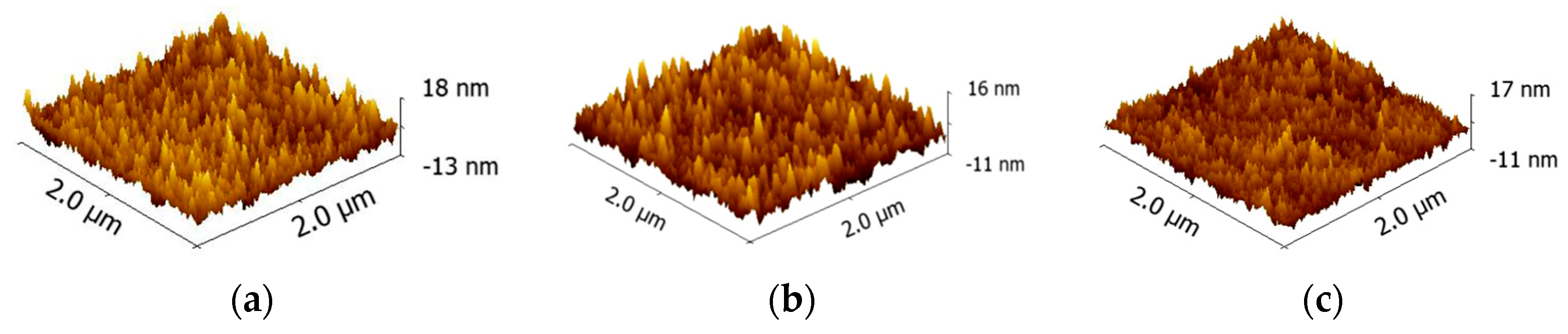
2.4. Atomic Force Microscopy
2.5. X-ray Photoelectron Spectroscopy
2.6. Ultraviolet Photoelectron Spectroscopy
3. Materials and Methods
3.1. Materials
3.2. OPV Device Fabrication
3.3. Current-Density Characterisation
3.4. Atomic Force Microscopy
3.5. Photoelectron Spectroscopy
3.6. Absorption Spectroscopy
4. Conclusions
Acknowledgments
Author Contributions
Conflicts of Interest
References
- Timilsina, G.R.; Kurdgelashvili, L.; Narbel, P.A. Solar energy: Markets, economics and policies. Renew. Sustain. Energy Rev. 2012, 16, 449–465. [Google Scholar] [CrossRef]
- Nielsen, T.D.; Cruickshank, C.; Foged, S.; Thorsen, J.; Krebs, F.C. Business, market and intellectual property analysis of polymer solar cells. Sol. Energy Mater. Sol. Cells 2010, 94, 1553–1571. [Google Scholar] [CrossRef]
- Li, G.; Zhu, R.; Yang, Y. Polymer solar cells. Nat. Photonics 2012, 6, 153–161. [Google Scholar] [CrossRef]
- Shah, A.; Torres, P.; Tscharner, R.; Wyrsch, N.; Keppner, H. Photovoltaic technology: The case for thin-film solar cells. Science 1999, 285, 692–698. [Google Scholar] [CrossRef] [PubMed]
- Guenes, S.; Neugebauer, H.; Sariciftci, N.S. Conjugated polymer-based organic solar cells. Chem. Rev. 2007, 107, 1324–1338. [Google Scholar] [CrossRef] [PubMed]
- Delgado, J.L.; Bouit, P.A.; Filippone, S.; Herranz, M.A.; Martin, N. Organic photovoltaics: A chemical approach. Chem. Commun. 2010, 46, 4853–4865. [Google Scholar] [CrossRef] [PubMed]
- Liu, Y.; Zhao, J.; Li, Z.; Mu, C.; Ma, W.; Hu, H.; Jiang, K.; Lin, H.; Ade, H.; Yan, H. Aggregation and morphology control enables multiple cases of high-efficiency polymer solar cells. Nat. Commun. 2014, 5. [Google Scholar] [CrossRef] [PubMed]
- Steim, R.; Kogler, F.R.; Brabec, C.J. Interface materials for organic solar cells. J. Mater. Chem. 2010, 20, 2499–2512. [Google Scholar] [CrossRef]
- Arias, A.C.; Granstrom, M.; Thomas, D.S.; Petritsch, K.; Friend, R.H. Doped conducting-polymer-semiconducting-polymer interfaces: Their use in organic photovoltaic devices. Phys. Rev. B 1999, 60, 1854–1860. [Google Scholar] [CrossRef]
- Ko, C.J.; Lin, Y.K.; Chen, F.C.; Chu, C.W. Modified buffer layers for polymer photovoltaic devices. Appl. Phys. Lett. 2007, 90. [Google Scholar] [CrossRef]
- Lee, K.; Kim, J.Y.; Park, S.H.; Kim, S.H.; Cho, S.; Heeger, A.J. Air-stable polymer electronic devices. Adv. Mater. 2007, 19. [Google Scholar] [CrossRef]
- Norrman, K.; Madsen, M.V.; Gevorgyan, S.A.; Krebs, F.C. Degradation patterns in water and oxygen of an inverted polymer solar cell. J. Am. Chem. Soc. 2010, 132, 16883–16892. [Google Scholar] [CrossRef] [PubMed]
- Ratcliff, E.L.; Zacher, B.; Armstrong, N.R. Selective inter layers and contacts in organic photovoltaic cells. J. Phys. Chem. Lett. 2011, 2, 1337–1350. [Google Scholar] [CrossRef] [PubMed]
- De Jong, M.P.; van Ijzendoorn, L.J.; de Voigt, M.J.A. Stability of the interface between indium-tin-oxide and poly(3,4-ethylenedioxythiophene)/poly(styrenesulfonate) in polymer light-emitting diodes. Appl. Phys. Lett. 2000, 77, 2255–2257. [Google Scholar] [CrossRef]
- Shrotriya, V.; Li, G.; Yao, Y.; Chu, C.W.; Yang, Y. Transition metal oxides as the buffer layer for polymer photovoltaic cells. Appl. Phys. Lett. 2006, 88. [Google Scholar] [CrossRef]
- Park, J.H.; Lee, T.W.; Chin, B.D.; Wang, D.H.; Park, O.O. Roles of interlayers in efficient organic photovoltaic devices. Macromol. Rapid Commun. 2010, 31, 2095–2108. [Google Scholar] [CrossRef] [PubMed]
- Chen, S.; Manders, J.R.; Tsang, S.W.; So, F. Metal oxides for interface engineering in polymer solar cells. J. Mater. Chem. 2012, 22, 24202–24212. [Google Scholar] [CrossRef]
- Wang, H.Q.; Li, N.; Guldal, N.S.; Brabec, C.J. Nanocrystal V2O5 thin film as hole-extraction layer in normal architecture organic solar cells. Org. Electron. 2012, 13, 3014–3021. [Google Scholar] [CrossRef]
- Chambers, B.A.; MacDonald, B.I.; Ionescu, M.; Deslandes, A.; Quinton, J.S.; Jasieniak, J.J.; Andersson, G.G. Examining the role of ultra-thin atomic layer deposited metal oxide barrier layers on cdte/ito interface stability during the fabrication of solution processed nanocrystalline solar cells. Sol. Energy Mater. Sol. Cells 2014, 125, 164–169. [Google Scholar] [CrossRef]
- Townsend, T.K.; Yoon, W.; Foos, E.E.; Tischler, J.G. Impact of nanocrystal spray deposition on inorganic solar cells. ACS Appl. Mater. Interfaces 2014, 6, 7902–7909. [Google Scholar] [CrossRef] [PubMed]
- Kim, A.; Won, Y.; Woo, K.; Jeong, S.; Moon, J. All-solution-processed indium-free transparent composite electrodes based on Ag nanowire and metal oxide for thin- film solar cells. Adv. Funct. Mater. 2014, 24, 2462–2471. [Google Scholar] [CrossRef]
- Song, S.H.; Aydil, E.S.; Campbell, S.A. Metal-oxide broken-gap tunnel junction for copper indium gallium diselenide tandem solar cells. Sol. Energy Mater. Sol. Cells 2015, 133, 133–142. [Google Scholar] [CrossRef]
- Gwinner, M.C.; di Pietro, R.; Vaynzof, Y.; Greenberg, K.J.; Ho, P.K.H.; Friend, R.H.; Sirringhaus, H. Doping of organic semiconductors using molybdenum trioxide: A quantitative time-dependent electrical and spectroscopic study. Adv. Funct. Mater. 2011, 21, 1432–1441. [Google Scholar] [CrossRef]
- Zilberberg, K.; Trost, S.; Meyer, J.; Kahn, A.; Behrendt, A.; Luetzenkirchen-Hecht, D.; Frahm, R.; Riedl, T. Inverted organic solar cells with sol-gel processed high work-function vanadium oxide hole-extraction layers. Adv. Funct. Mater. 2011, 21, 4776–4783. [Google Scholar] [CrossRef]
- Zilberberg, K.; Trost, S.; Schmidt, H.; Riedl, T. Solution processed vanadium pentoxide as charge extraction layer for organic solar cells. Adv. Energy Mater. 2011, 1, 377–381. [Google Scholar] [CrossRef]
- Tan, Z.A.; Zhang, W.Q.; Cui, C.H.; Ding, Y.Q.; Qian, D.P.; Xu, Q.; Li, L.J.; Li, S.S.; Li, Y.F. Solution-processed vanadium oxide as a hole collection layer on an ito electrode for high-performance polymer solar cells. Phys. Chem. Chem. Phys. 2012, 14, 14589–14595. [Google Scholar] [CrossRef] [PubMed]
- Xie, F.X.; Choy, W.C.H.; Wang, C.D.; Li, X.C.; Zhang, S.Q.; Hou, J.H. Low-temperature solution-processed hydrogen molybdenum and vanadium bronzes for an efficient hole-transport layer in organic electronics. Adv. Mater. 2013, 25, 2051–2055. [Google Scholar] [CrossRef] [PubMed]
- Jin, S.; Jung, B.J.; Song, C.K.; Kwak, J. Room-temperature and solution-processed vanadium oxide buffer layer for efficient charge injection in bottom-contact organic field-effect transistors. Curr. Appl. Phys. 2014, 14, 1809–1812. [Google Scholar] [CrossRef]
- Oksuzoglu, R.M.; Bilgic, P.; Yildirim, M.; Deniz, O. Influence of post-annealing on electrical, structural and optical properties of vanadium oxide thin films. Opt. Laser Technol. 2013, 48, 102–109. [Google Scholar] [CrossRef]
- Sahana, M.B.; Sudakar, C.; Thapa, C.; Lawes, G.; Naik, V.M.; Baird, R.J.; Auner, G.W.; Naik, R.; Padmanabhan, K.R. Electrochemical propertiesof V2O5 thin films deposited by spin coating. Mater. Sci. Eng. B 2007, 143, 42–50. [Google Scholar] [CrossRef]
- Haber, J.; Witko, M.; Tokarz, R. Vanadium pentoxide.1. Structures and properties. Appl. Catal. A Gen. 1997, 157, 3–22. [Google Scholar] [CrossRef]
- Watters, D.C.; Yi, H.; Pearson, A.J.; Kingsley, J.; Iraqi, A.; Lidzey, D. Fluorene-based co-polymer with high hole mobility and device performance in bulk heterojunction organic solar cells. Macromol. Rapid Commun. 2013, 34, 1157–1162. [Google Scholar] [CrossRef] [PubMed]
- Lu, L.; Xu, T.; Chen, W.; Landry, E.S.; Yui, L. Ternary blend polymer solar cells with enhanced power conversion efficiency. Nat. Photonics 2014, 8, 716–722. [Google Scholar] [CrossRef]
- Zilberberg, K.; Meyer, J.; Riedl, T. Solution processed metal-oxides for organic electronic devices. J. Mater. Chem. C 2013, 1, 4796–4815. [Google Scholar] [CrossRef]
- Wagenpfahl, A.; Rauh, D.; Binder, M.; Deibel, C.; Dyakonov, V. S-shaped current-voltage characteristics of organic solar devices. Phys. Rev. B 2010, 82, 115306. [Google Scholar] [CrossRef]
- Kim, J.; Kim, H.; Kim, G.; Back, H.; Lee, K. Soluble transition metal oxide/polymeric acid composites for efficient hole-transport layers in polymer solar cells. ACS Appl. Mater. Interfaces 2014, 6, 951–957. [Google Scholar] [CrossRef] [PubMed]
- Talledo, A.; Granqvist, C.G. Electrochromic vanadium-pentoxide-based films—Structural, electrochemical, and optical-properties. J. Appl. Phys. 1995, 77, 4655–4666. [Google Scholar] [CrossRef]
- Bullot, J.; Cordier, P.; Gallais, O.; Gauthier, M.; Babonneau, F. Thin-layers deposited from V2O5 gels 2. An optical-absorption study. J. Non Cryst. Solids 1984, 68, 135–146. [Google Scholar] [CrossRef]
- Meyer, J.; Zilberberg, K.; Riedl, T.; Kahn, A. Electronic structure of vanadium pentoxide: An efficient hole injector for organic electronic materials. J. Appl. Phys. 2011, 110, 033710–033715. [Google Scholar] [CrossRef]
- Hancox, I.; Rochford, L.A.; Clare, D.; Walker, M.; Mudd, J.J.; Sullivan, P.; Schumann, S.; McConville, C.F.; Jones, T.S. Optimization of a high work function solution processed vanadium oxide hole-extracting layer for small molecule and polymer organic photovoltaic cells. J. Phys. Chem. C 2013, 117, 49–57. [Google Scholar] [CrossRef]
- Negreira, A.S.; Aboud, S.; Wilcox, J. Surface reactivity of V2O5(001): Effects of vacancies, protonation, hydroxylation, and chlorination. Phys. Rev. B 2011, 83. [Google Scholar] [CrossRef]
- Silversmit, G.; Depla, D.; Poelman, H.; Marin, G.B.; de Gryse, R. Determination of the V2p XPS binding energies for different vanadium oxidation states (V5+ to V0+). J. Electron Spectrosc. Relat. Phenom. 2004, 135, 167–175. [Google Scholar] [CrossRef]
- Sawatzky, G.A.; Post, D. X-ray photoelectron and auger-spectroscopy study of some vanadium-oxides. Phys. Rev. B 1979, 20, 1546–1555. [Google Scholar] [CrossRef]
- Demeter, M.; Neumann, M.; Reichelt, W. Mixed-valence vanadium oxides studied by XPS. Surf. Sci. 2000, 454–456, 41–44. [Google Scholar] [CrossRef]
- Coulston, G.W.; Thompson, E.A.; Herron, N. Characterization of vpo catalysts by X-ray photoelectron spectroscopy. J. Catal. 1996, 163, 122–129. [Google Scholar] [CrossRef]
- Suchorski, Y.; Rihko-Struckmann, L.; Klose, F.; Ye, Y.; Alandjiyska, M.; Sundmacher, K.; Weiss, H. Evolution of oxidation states in vanadium-based catalysts under conventional XPS conditions. Appl. Surf. Sci. 2005, 249, 231–237. [Google Scholar] [CrossRef]
- Hermann, K.; Witko, M.; Druzinic, R.; Tokarz, R. Hydrogen assisted oxygen desorption from the V2O5(010) surface. Top. Catal. 2000, 11, 67–75. [Google Scholar] [CrossRef]
- Toledano, D.S.; Henrich, V.E.; Metcalf, P. Surface reduction of Cr-V2O3 by Co. J. Vacuum Sci. Technol. A 2000, 18, 1906–1914. [Google Scholar] [CrossRef]
- Ganduglia-Pirovano, M.V.; Sauer, J. Stability of reduced V2O5(001) surfaces. Phys. Rev. B 2004, 70. [Google Scholar] [CrossRef]
- Yuan, N.Y.; Li, J.H.; Lin, C.L. Valence reduction process from sol-gel V2O5 to VO2 thin films. Appl. Surf. Sci. 2002, 191, 176–180. [Google Scholar]
- Surnev, S.; Ramsey, M.G.; Netzer, F.P. Vanadium oxide surface studies. Prog. Surf. Sci. 2003, 73, 117–165. [Google Scholar] [CrossRef]
- Bermudez, V.M.; Williams, R.T.; Long, J.P.; Reed, R.K.; Klein, P.H. Photoemission-study of hydrogen adsorption on vanadium dioxide near the semiconductor-metal phase-transition. Phys. Rev. B 1992, 45, 9266–9271. [Google Scholar] [CrossRef]
- Greiner, M.T.; Helander, M.G.; Tang, W.M.; Wang, Z.B.; Qiu, J.; Lu, Z.H. Universal energy-level alignment of molecules on metal oxides. Nat. Mater. 2012, 11, 76–81. [Google Scholar] [CrossRef] [PubMed]
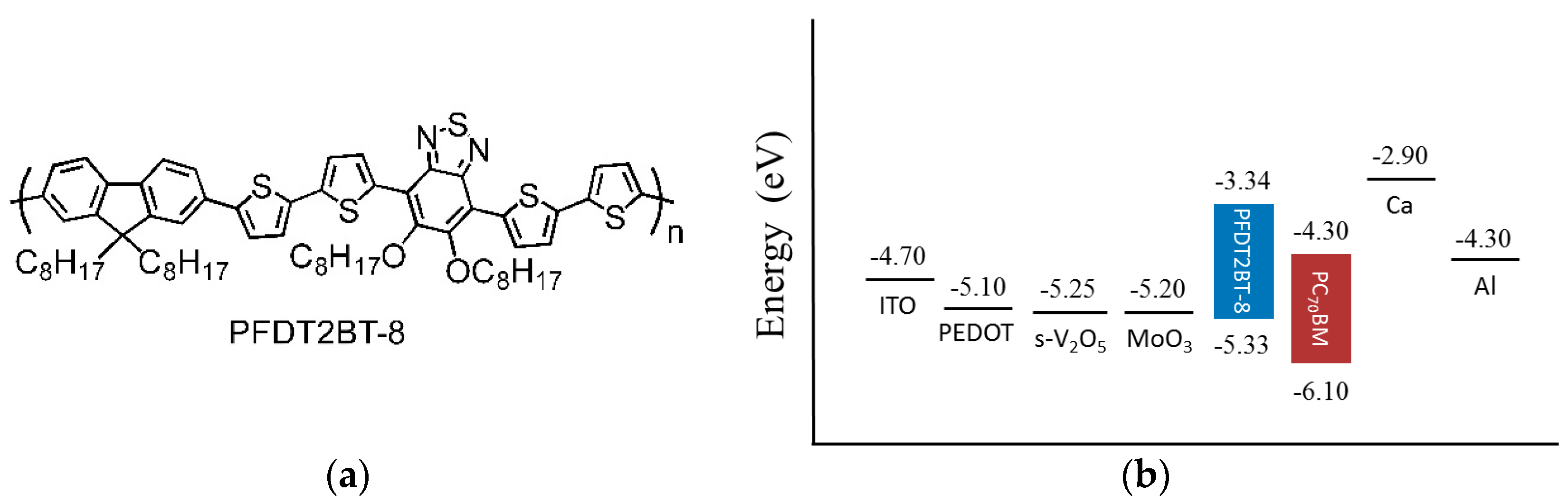
 ) s-V2Ox, and (
  ) MoO3.
) s-V2Ox, and ( ) MoO3.
) MoO3.
) s-V2Ox, and ( ) MoO3.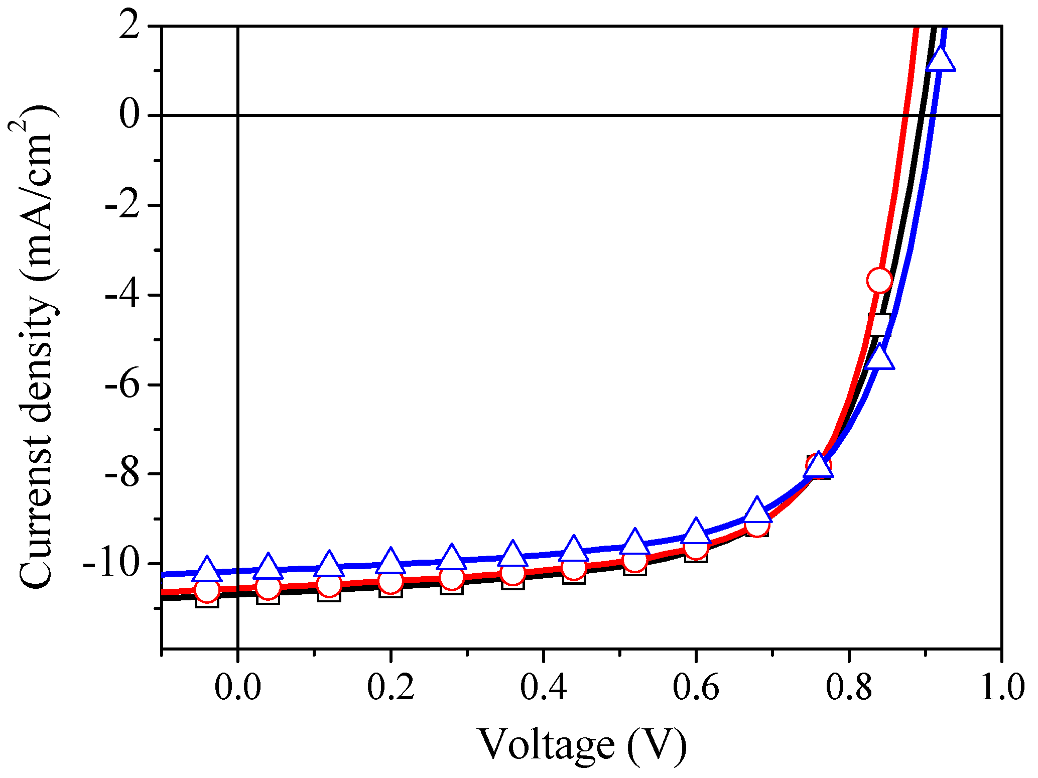 ) 100 °C, ( ) 200 °C, (
  ) 300 °C, and (
  ) 400 °C for 30 min.
) 100 °C, ( ) 200 °C, ( ) 300 °C, and ( ) 400 °C for 30 min.
) 400 °C for 30 min.
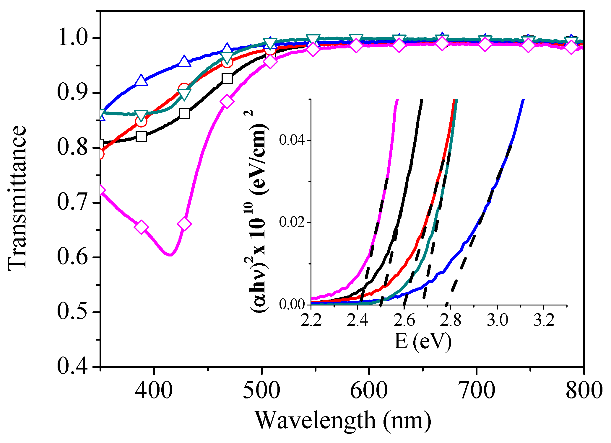
) 100 °C, ( ) 200 °C, ( ) 300 °C, and ( ) 400 °C for 30 min.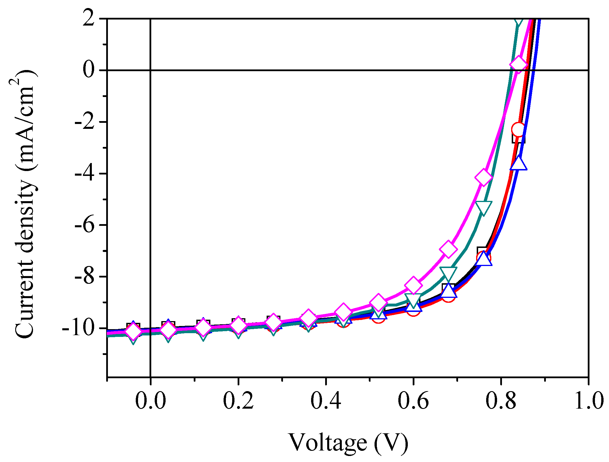 ) 100 °C, ( ) 200 °C, ( ) 300 °C, and ( ) 400 °C. The insert shows the absorption coefficient (αhν)2 as a function of the photon energy.
) 100 °C, ( ) 200 °C, ( ) 300 °C, and ( ) 400 °C. The insert shows the absorption coefficient (αhν)2 as a function of the photon energy.
) 100 °C, ( ) 200 °C, ( ) 300 °C, and ( ) 400 °C. The insert shows the absorption coefficient (αhν)2 as a function of the photon energy.
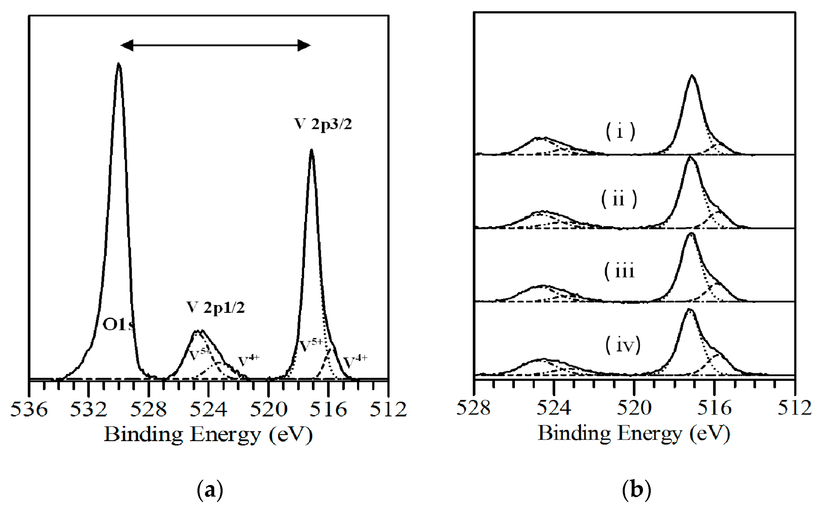 ) 200 °C, ( ) 300 °C, and ( ) 400 °C. (a) shows the secondary electron cut-off region; and (b) shows the expanded region near the Fermi level; the insert shows the density of gap states formed about 1 eV below the Fermi level.
) 200 °C, ( ) 300 °C, and ( ) 400 °C. (a) shows the secondary electron cut-off region; and (b) shows the expanded region near the Fermi level; the insert shows the density of gap states formed about 1 eV below the Fermi level.
) 200 °C, ( ) 300 °C, and ( ) 400 °C. (a) shows the secondary electron cut-off region; and (b) shows the expanded region near the Fermi level; the insert shows the density of gap states formed about 1 eV below the Fermi level.

| Ann. Temp. | Maximum PCE (%) | Average PCE(av) (%) | Voc (V) | Jsc (mA·cm−2) | FF (%) | Rs (Ω·cm2) | Rsh (Ω·cm2) |
|---|---|---|---|---|---|---|---|
| Non | 6.0 | 5.8 ± 0.14 | 0.86 | 10.0 ± 0.22 | 67.1 ± 1.2 | 11.6 ± 0.9 | 1264 ± 91 |
| 100 | 6.0 | 5.9 ± 0.14 | 0.86 | 10.1 ± 0.13 | 68.3 ± 1.7 | 10.5 ± 1.0 | 1282 ± 215 |
| 200 | 6.3 | 5.9 ± 0.26 | 0.87 | 10.2 ± 0.14 | 67.1 ± 2.6 | 10.3 ± 0.7 | 1346 ± 246 |
| 300 | 5.6 | 5.3 ± 0.28 | 0.83 | 9.9 ± 0.41 | 64.3 ± 2.7 | 12.6 ± 1.7 | 1095 ± 238 |
| 400 | 5.2 | 5.0 ± 0.17 | 0.83 | 10.1 ± 0.12 | 59.6 ± 0.9 | 17.6 ± 0.4 | 933 ± 84 |
| Annealing Temperature | V4+ Oxidation State | V5+ Oxidation State | Work Function (eV) | Valence Band (eV) | Eg (eV) |
|---|---|---|---|---|---|
| Unannealing | 15% | 85% | 5.26 | 2.53 | 2.5 |
| 200 °C | 22.5% | 77.5% | 5.22 | 2.53 | 3.78 |
| 300 °C | 27% | 73% | 5.23 | 2.50 | 2.68 |
| 400 °C | 33% | 67% | 5.19 | 2.50 | 2.42 |
© 2016 by the authors; licensee MDPI, Basel, Switzerland. This article is an open access article distributed under the terms and conditions of the Creative Commons by Attribution (CC-BY) license (http://creativecommons.org/licenses/by/4.0/).
Share and Cite
Alsulami, A.; Griffin, J.; Alqurashi, R.; Yi, H.; Iraqi, A.; Lidzey, D.; Buckley, A. Thermally Stable Solution Processed Vanadium Oxide as a Hole Extraction Layer in Organic Solar Cells. Materials 2016, 9, 235. https://doi.org/10.3390/ma9040235
Alsulami A, Griffin J, Alqurashi R, Yi H, Iraqi A, Lidzey D, Buckley A. Thermally Stable Solution Processed Vanadium Oxide as a Hole Extraction Layer in Organic Solar Cells. Materials. 2016; 9(4):235. https://doi.org/10.3390/ma9040235
Chicago/Turabian StyleAlsulami, Abdullah, Jonathan Griffin, Rania Alqurashi, Hunan Yi, Ahmed Iraqi, David Lidzey, and Alastair Buckley. 2016. "Thermally Stable Solution Processed Vanadium Oxide as a Hole Extraction Layer in Organic Solar Cells" Materials 9, no. 4: 235. https://doi.org/10.3390/ma9040235
APA StyleAlsulami, A., Griffin, J., Alqurashi, R., Yi, H., Iraqi, A., Lidzey, D., & Buckley, A. (2016). Thermally Stable Solution Processed Vanadium Oxide as a Hole Extraction Layer in Organic Solar Cells. Materials, 9(4), 235. https://doi.org/10.3390/ma9040235