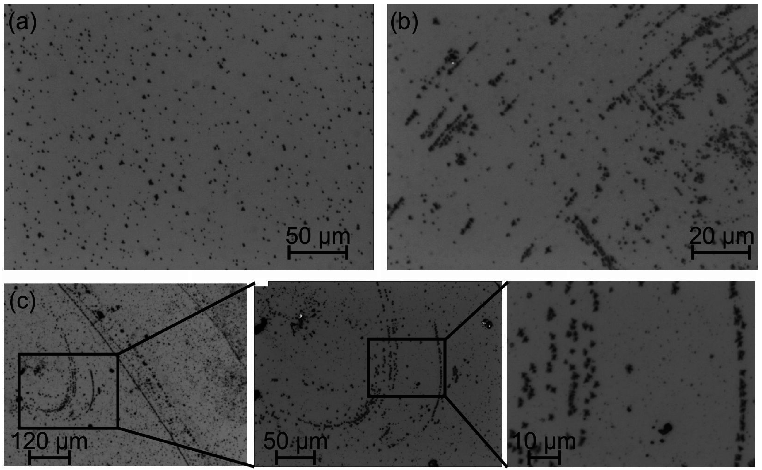
3.1. Substrate Morphology
The light microscope images (
Figure 1) show an overview of the substrate surface of the LGS heated for 48 h. A lot of small features are visible.
Figure 1a demonstrates a region with an isotropic distribution of the features while
Figure 1b shows an accumulation at scratches at the sample surface. The overview image of the 10 + 48 h LGS substrate in
Figure 1c shows neighboring sample regions with homogeneous distribution of the features and with agglomeration at the scratches. The zoomed images clarify that the occurrence of the features follows the path of the scratches. This observation leads to the assumption that the features preferably form at points where there is a damage or inhomogeneity in the single crystal lattice.
Figure 1.
Light microscope image of the 48 h preheated LaGaSiO (LGS) substrate showing (a) a region with homogeneous distribution; and (b) the agglomeration of the features along scratches at the sample surface; (c) Overview image the 10 + 48 h LGS substrate together with zoom images showing agglomeration of the features at scratches.
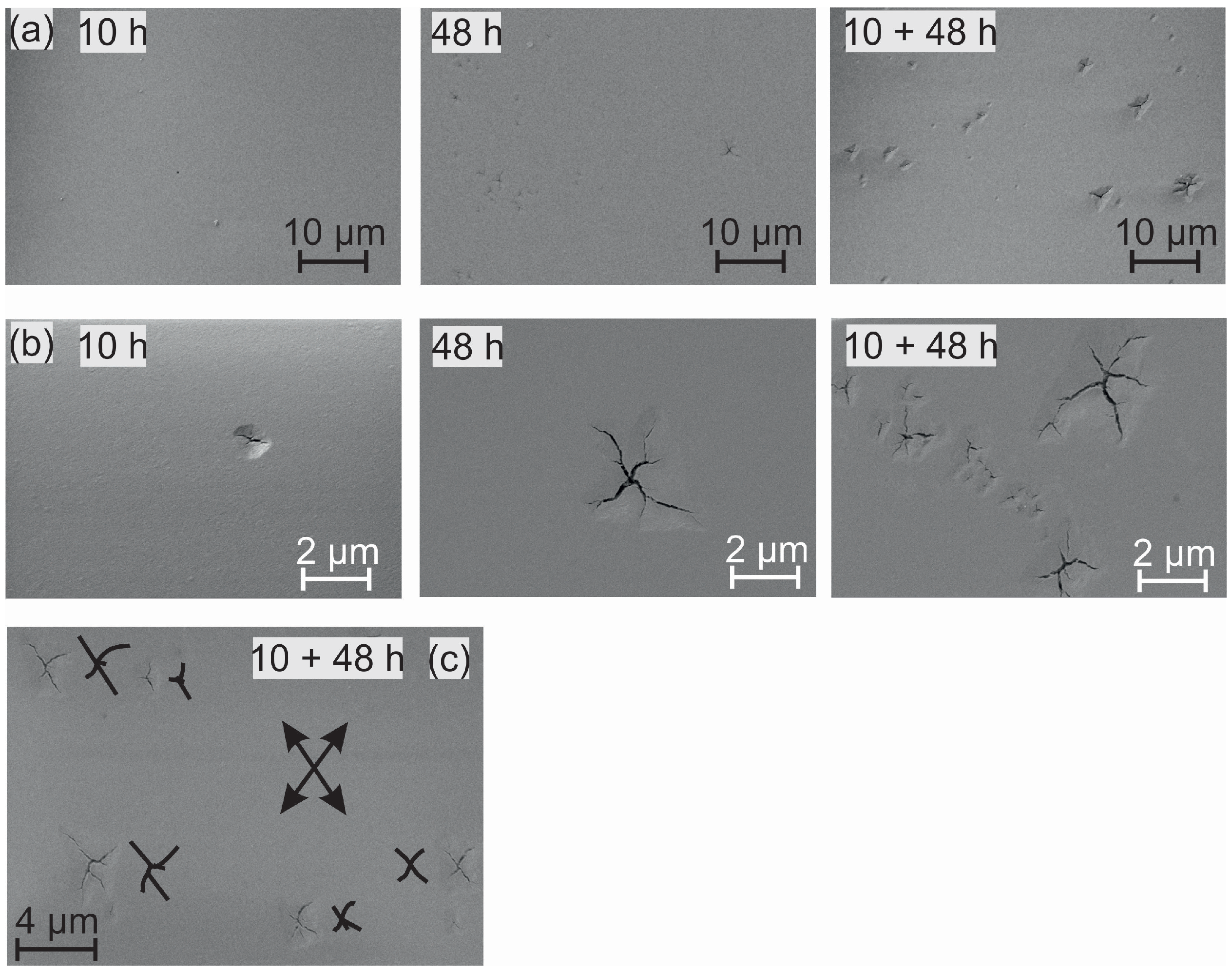
To reveal the nature of the features, investigations with scanning electron microscopy have been performed. Images with two different magnifications are presented in
Figure 2a,b. The high magnification image clarifies that the features are cracks in the surface of the substrate. For the short heating time of 10 h, hardly any changes are found on the surface, only very few small cracks appear. For the longer heated samples, the area density of such cracks strongly increases. As it can be seen in the higher magnification images in
Figure 2b, also the size of these features becomes larger with increasing heating time. Additionally it appears that the alignment of the cracks at the substrate surface is not random. In most of the features, the direction of the cracks in the surface is quite the same, as is indicated by the arrows in
Figure 2c. In this image, for a better visibility the direction of the cracks is outlined by the sketch next to the features. It has to be assumed that there is a correlation with the crystal structure.
LGS crystals were developed about 30 years ago. It is known that these crystals are not completely homogeneous, so differences in composition and properties occur [
11]. Ga and Si may occupy same positions and also oxygen vacancies are present. These variations in composition also lead to differences in the color of the LGS crystals. Kuzmicheva,
et al. showed that in Czochralski-grown LGS crystals the composition may vary both axially and radially [
12]. They also showed the coexistence of two isostrucutral solid solutions [
12]. Capelle,
et al. summarize that the dominant inhomogeneities in LGS are dislocations, growth bands and inclusions and that recently crystals with a reduced density of dislocations and inclusions were prepared [
11]. Wang and Uda investigated the homogeneity of LGS with a bulk-wave-measurement and showed that the sound velocity varies across the wafer. They also conclude that there is a need for an improvement of the crystal growth [
13]. In summary, there exist a lot of inhomogeneities which can support the formation of diffusion channels and the development of such cracks. Moreover, inhomogeneities which are introduced from outside, like small scratches from the sawing of the wafers might additionally promote the formation of the observed features.
Figure 2.
SE-SEM images of the heated substrates at low (a) and high (b) magnification. (c) SE-SEM image of the 10 + 48 h sample. The arrows indicate the two main directions of the cracks in the substrate.
Figure 2.
SE-SEM images of the heated substrates at low (a) and high (b) magnification. (c) SE-SEM image of the 10 + 48 h sample. The arrows indicate the two main directions of the cracks in the substrate.
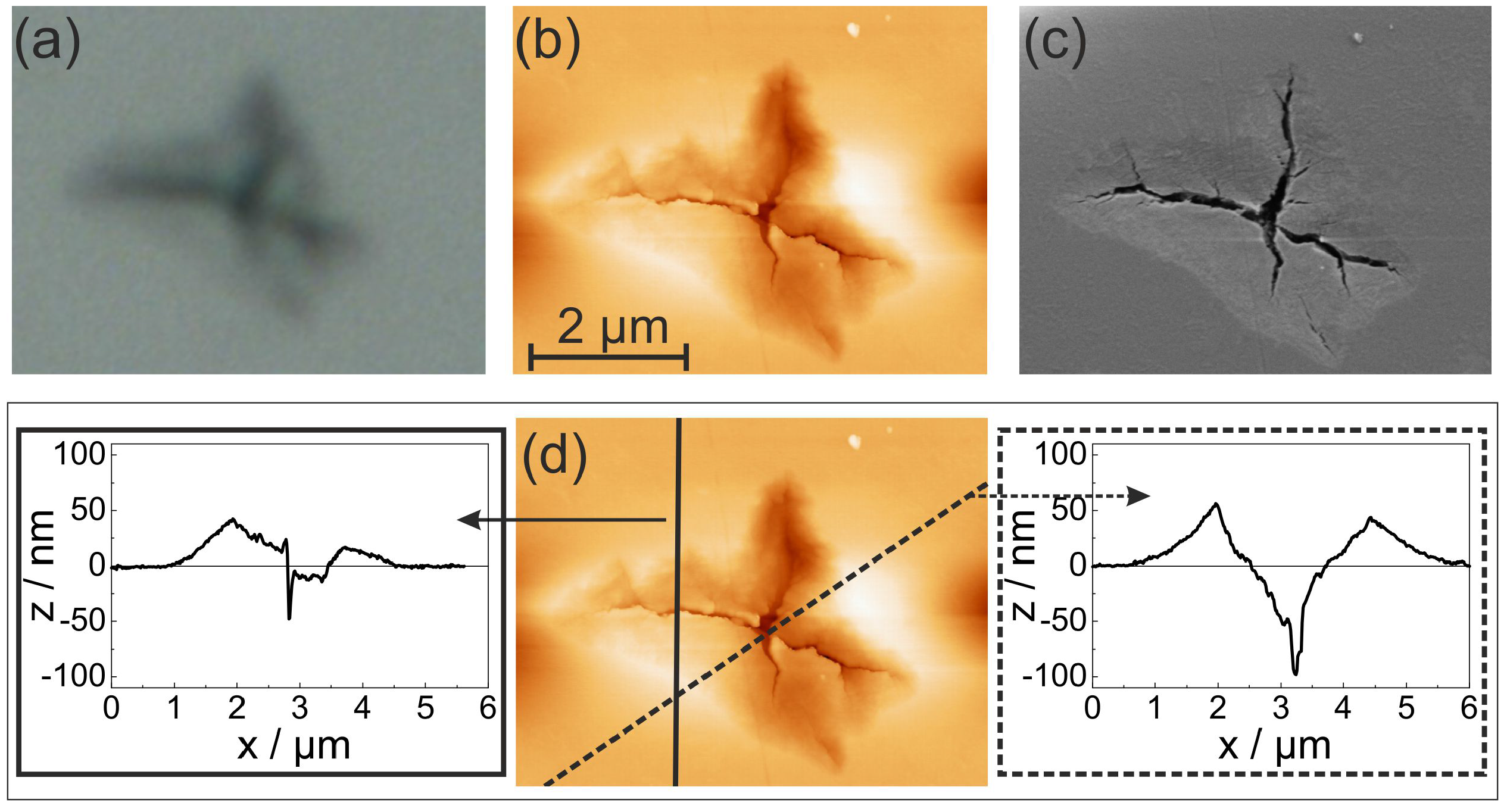
A comparison of light microscopy, atomic force microscopy and scanning electron microscopy of the same sample position (sample: 10 + 48 h) is presented in
Figure 3. The AFM image reveals the complicated surface morphology with elevations and subsidences of the surface around the crack. This can be quantified by line profiles of the AFM image, as presented in
Figure 3d. At the outer region of the structure, the surface is raised up to 60 nm, followed by a slope to the center of the crack. The deepest point measured by AFM of about minus 100 nm is of course limited by the geometry of the AFM tip and doesn’t reproduce the actual depth.
Figure 3.
(a) Light microscope; (b) atomic force microscopy (AFM); and (c) SE-SEM image of the same crack of the 10 + 48 h pretreated LGS substrate; (d) shows the AFM line profiles across the crack.
Figure 3.
(a) Light microscope; (b) atomic force microscopy (AFM); and (c) SE-SEM image of the same crack of the 10 + 48 h pretreated LGS substrate; (d) shows the AFM line profiles across the crack.
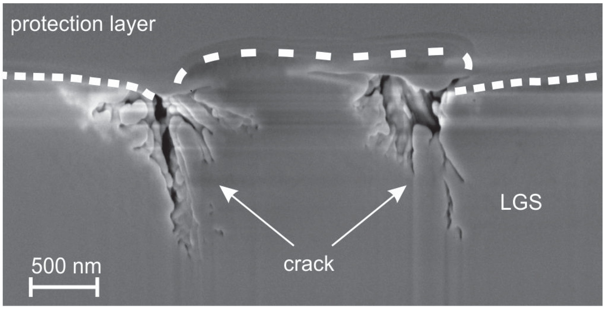
To get more information about the real depth of the cracks, cross sections were analyzed. An SEM in-lens image of such a cross section of a crack is presented in
Figure 4. It shows that these cracks are extended to a huge network of channels below the surface of the substrate. They reach a depth of more than 1 μm. This finding resembles the formation of voids near the LGS substrate surface of a SAW device in uncovered areas between the finger electrodes after a heat treatment at 650
C in light vacuum (0.4 mbar) observed by Bardong,
et al. [
10].
Figure 4.
In-lens SEM image of a crack in the 10 + 48 h heated LGS substrate. The dashed line serves as guide to the eye for the interface between LGS substrate and protection layer which was deposited for the FIB process.
Figure 4.
In-lens SEM image of a crack in the 10 + 48 h heated LGS substrate. The dashed line serves as guide to the eye for the interface between LGS substrate and protection layer which was deposited for the FIB process.
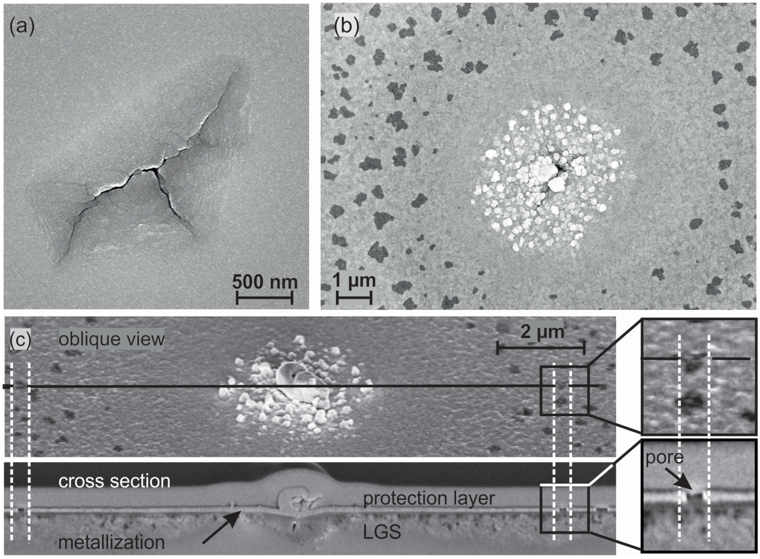
3.2. Influence of LGS Annealing on RuAl Thin Films
As an example, the LGS 10 + 48 h pretreated substrates covered with a 110 nm RuAl metallization will be discussed in this section.
Figure 5a shows an image of such a sample in the as-deposited state of the metallization. A homogeneous smooth film with fine grains has formed and the crack is clearly visible. The morphology of the film strongly changes after annealing at 800
C for 10 h under high vacuum (
Figure 5b, different sample position).
Figure 5.
In-lens SEM image of a RuAl thin film deposited on a pretreated LGS substrate (a) before; and (b) after annealing at 800 C under high vacuum conditions at the position of a crack in the LGS (both images not showing the same sample position); (c) In-lens SEM image of such a feature taken in the FIB device together with an In-lens SEM image of a FIB cut through it.
Clearly visible is the crack in the center of the image, but the metallization is not homogeneous any more. The crack is surrounded by bright structures which seem to be grown out of the film. Around this area, there is a homogeneous ring followed by an area with dark structures.
Figure 5c shows an image of such a feature taken in the FIB device together with a FIB cross section across the center of the crack, the homogeneous ring around it and through the region with the dark spots. In the center, huge structures have grown out of the film. Around the center, the metallization is continuous. In larger distance to the center, it can be seen that at the positions where the FIB cut goes through such a dark structure there is a pore within the metallization. Former investigation of RuAl films directly deposited on untreated LGS substrates and annealed at 800
C proved a complete demixing of the RuAl alloy in an Al
O
layer above the substrate, followed by a nearly pure Ru layer and with a thinner Al
O
layer on top [
14]. Pores were found within the Ru layer, while both Al
O
layers are continuous. The same behaviour is now determined for the film in a distance to the cracks, while near to the cracks there are no pores.
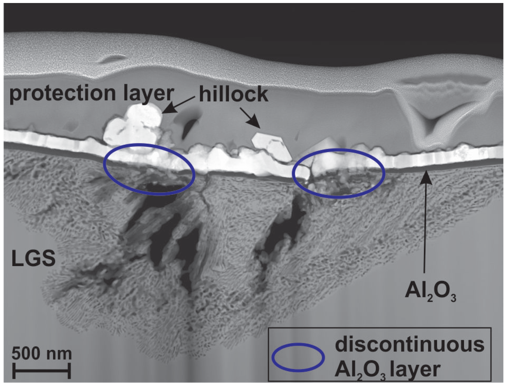
Figure 6 shows the high-angle annular dark field scanning transmission electron microscopy image of a cross section of such a structure. The large cracks are clearly visible. They are surrounded by a huge network of finer channels. At this position, the network has a depth of 1.6 μm and a width of about 4 μm. Above this channel-region, huge hillocks grow out of the metallic film. Although the metallization was deposited with a thickness of about 110 nm, these hillocks are up to 400 nm high.
Figure 6.
High-angle annular dark field scanning transmission electron microscopy (HAADF-STEM) image of the RuAl film on the pretreated LGS substrate (10 + 48 h) after annealing at 800 C for 10 h in high vacuum.
Figure 6.
High-angle annular dark field scanning transmission electron microscopy (HAADF-STEM) image of the RuAl film on the pretreated LGS substrate (10 + 48 h) after annealing at 800 C for 10 h in high vacuum.
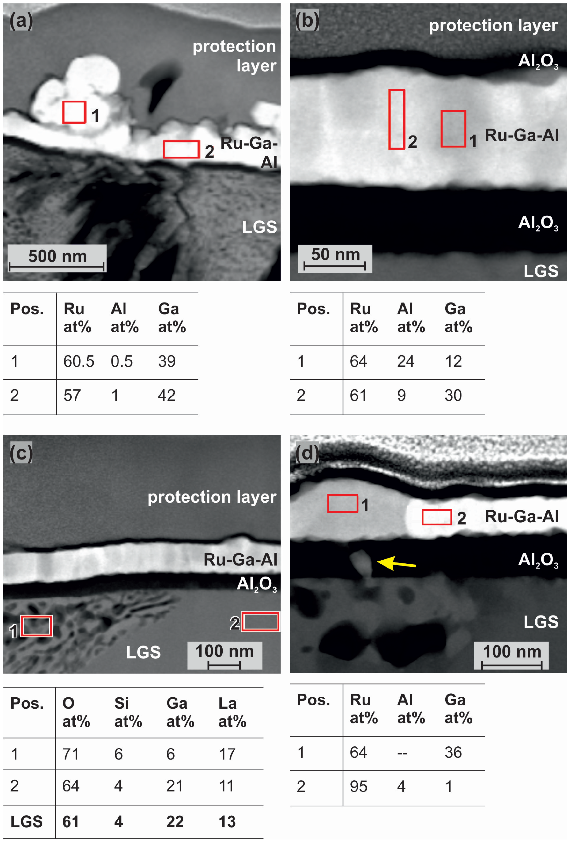
It can be seen that an Al
O
layer has formed between the substrate and the metallic film, which is continuous in larger distance to the cracks (see right region of the image), but which is disturbed and not continuous directly at the position of the cracks. These positions are marked with the blue circles. It is obvious, that the hillocks form exactly at those positions where the Al
O
layer is discontinuous. The EDX measurements show that the hillocks have a composition of about 60
% Ru and 40
% Ga (
Figure 7a). Above the zone of the channel network, the metallic layer also has the composition of 60
% Ru, while the residual 40
% are partly Ga and Al (
Figure 7b). As was shown by Seifert,
et al. for RuAl films deposited on thermally oxidized Si besides Ru rich grains, a Ru
Al
phase was most dominant after annealing at 800
C under high vacuum conditions [
14]. For the films now prepared on the pretreated substrates, we find the composition Ru
Al
Ga
. Although no phase diagram is known for the system Ru-Ga, several Ru-Ga phases have been determined. Among them exists the RuGa phase, which has the same crystal structure like RuAl [
15]. Altogether, this leads to the assumption that if the Al
O
layer on top of the LGS substrate is not continuous, it allows a strong diffusion of Ga from the substrate into the upper metallic film. There, Ga replaces Al within the RuAl phase, which is oxidized by O diffusing out of the substrate and forming the Al
O
layer at the interface to the substrate.
Figure 7.
Energy dispersive X-ray spectroscopy (EDX) measurements of the RuAl film deposited on the pretreated substrate after annealing at 800 C for 10 h. (a) at a position at the center of the crack; and (b) near to the crack; (c) EDX measurement of the LGS substrate in the region of the channels and in an undisturbed region; (d) EDX measurement of the RuAl film at a position where the AlO layer is disturbed. The yellow arrow indicates an inhomogeneity within the AlO layer.
In a larger distance to the cracks, a complete oxidation of the Al atoms and the formation of a nearly pure Ru layer is similarly found for the samples prepared on the pretreated substrates as compared to the untreated ones [
14]. As an example,
Figure 7d illustrates that only where the Al
O
layer is disturbed (see the bright contrast in Al
O
layer on the left hand side marked by the yellow arrow), a large amount of Ga diffuses into the Ru film and forms the RuGa phase. Close beside this point, the Al
O
layer is intact (right hand side), hardly allowing Ga to diffuse into the Ru film, resulting in a chemical composition of the metallic layer of 95
% Ru. The presence of small amounts of Ga in the Ru layer which formed after annealing a RuAl alloy on an untreated LGS substrate (under high vacuum conditions for 10 h at 800
C) was already shown in [
7].
The above described finding that there are no pores in the film near to the cracks but that pores are formed in larger distance to the cracks could be explained in the following way: the diffusion of Ga out of the substrate in the region of the cracks leads to the formation of a Ru-Al-Ga phase, whereas in larger distance to the cracks there is hardly any diffusion of Ga. In former work, the formation of pores was described as a stress relaxation mechanism due to the outwards diffusion of the Al atoms [
14]. Due to the inwards diffusion of Ga these stresses do not occur and no pores are formed—in contrast to the positions where the RuAl layer has demixed and no Ga has diffused into the film. Therefore, the pores are only found in larger distances to the cracks.
The analysis of the substrate composition in the range of the channels and in an undisturbed area shows that the Ga content is strongly decreased in the first case (
Figure 7c). This is consistent with the large Ga content within the metallic film. At farther distance from the cracks, the composition of the LGS corresponds quite well to the stoichiometric value.
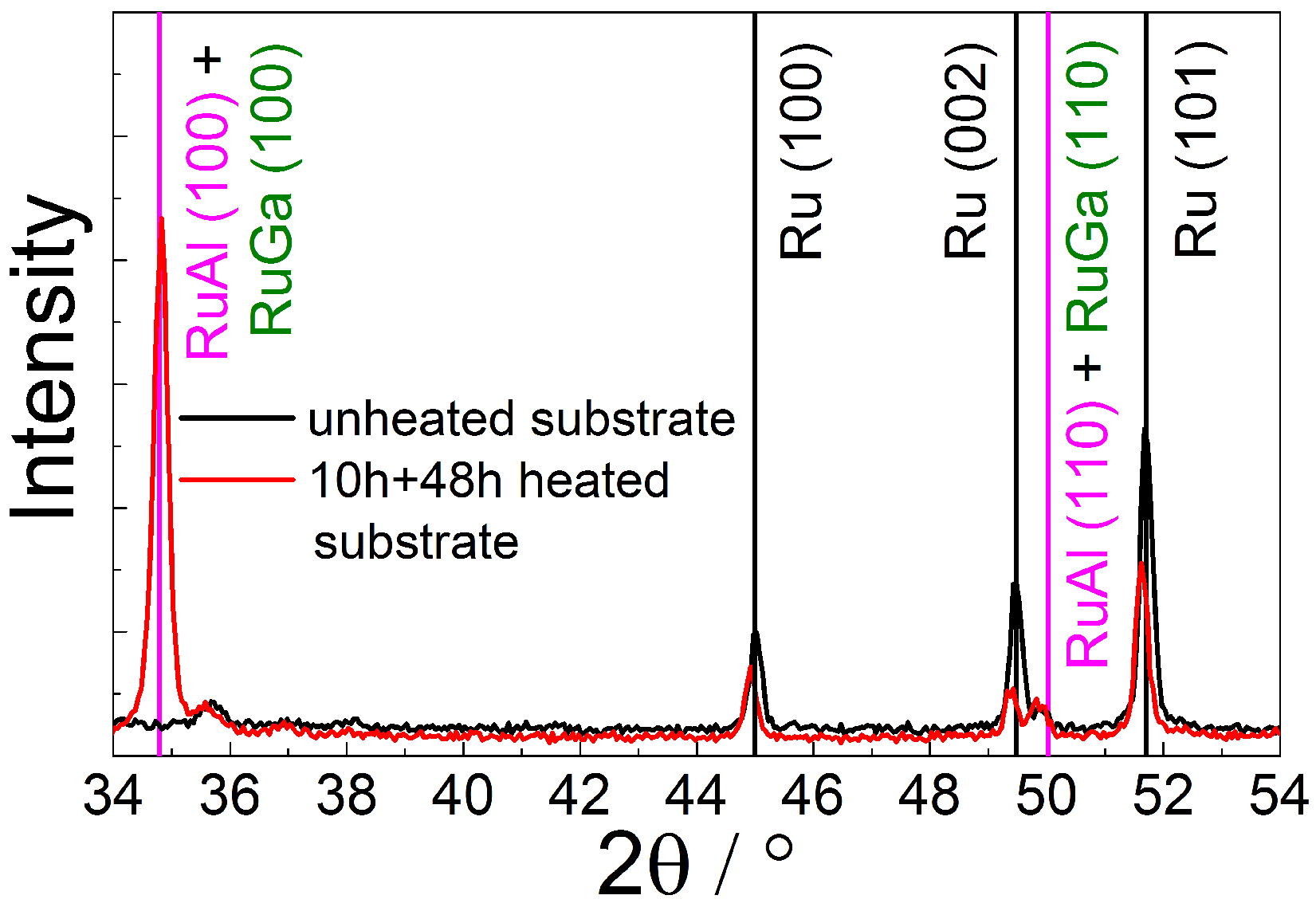
The XRD measurement of the heated RuAl sample on the 10 + 48 h pretreated substrate (
Figure 8) shows a peak at the position of the RuAl (100) reflex in contrast to a RuAl sample deposited on an untreated substrate and annealed at 800
C. In the latter case, the RuAl (100) is not present since all Al is oxidized and only a pure Ru layer has formed [
7]. Therefore, only Ru-reflexes appear in the XRD measurement. In contrast to this, as described above (
Section 3.2), the film on the pretreated substrate shows a chemical composition of Ru
Al
Ga
in the regions with the disturbed substrate and there is no complete demixing in Al
O
and pure Ru. Since RuAl and RuGa possess the same crystal structure, the strong reflex at 34.8
as well as the smaller reflex at 49.9
might be caused by a RuAl, RuGa or Ru-Al-Ga phase.
Figure 8.
X-ray diffraction (XRD) measurement of a RuAl thin film deposited on an unheated (black) and on a 10 + 48 h heated (red) LGS substrate after 10 h annealing at 800 C at high vacuum.
Figure 8.
X-ray diffraction (XRD) measurement of a RuAl thin film deposited on an unheated (black) and on a 10 + 48 h heated (red) LGS substrate after 10 h annealing at 800 C at high vacuum.


