Electrical Properties of CZO Films Prepared by Ultrasonic Spray Pyrolysis


Abstract
:1. Introduction
2. Results and Discussion
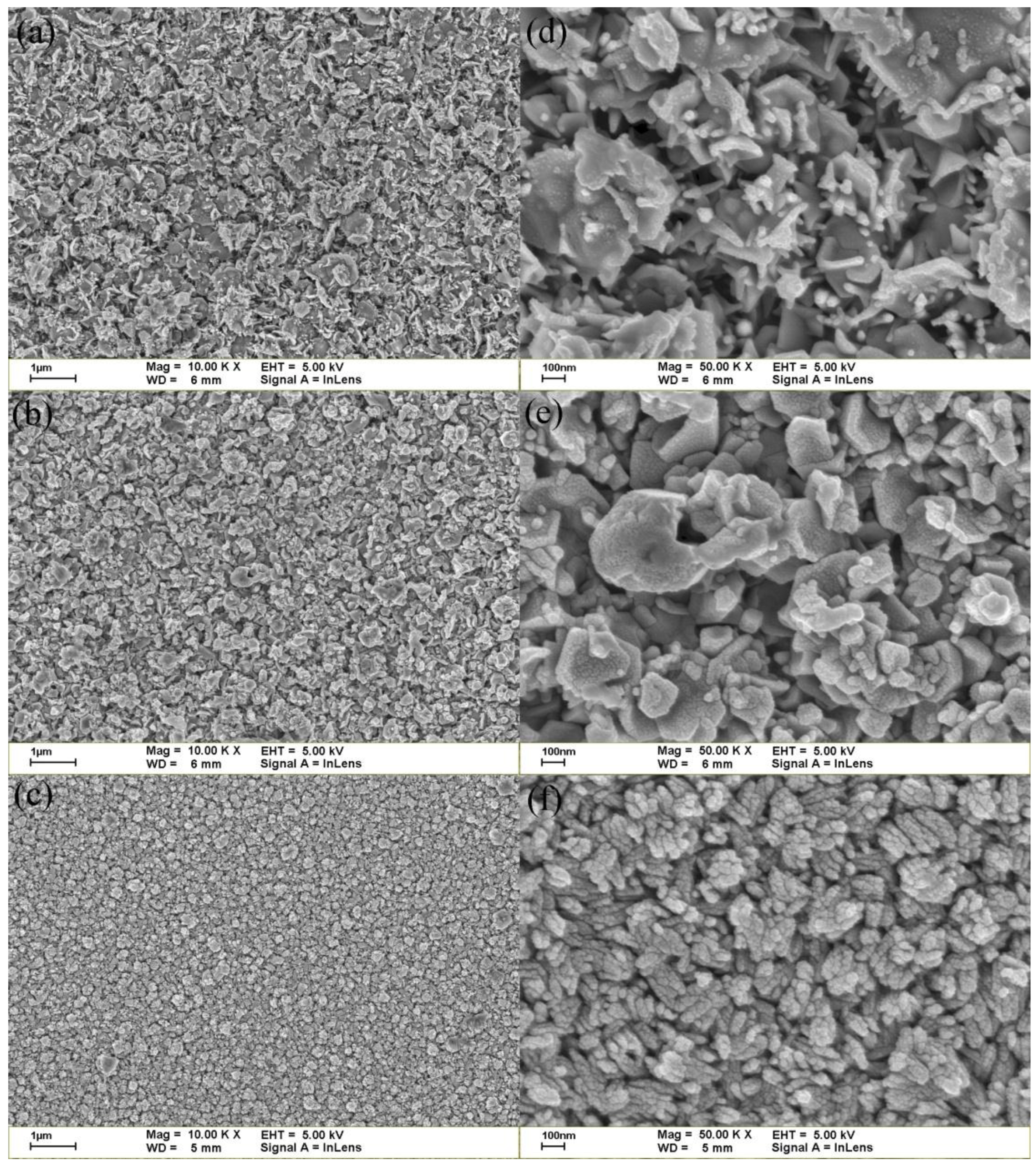
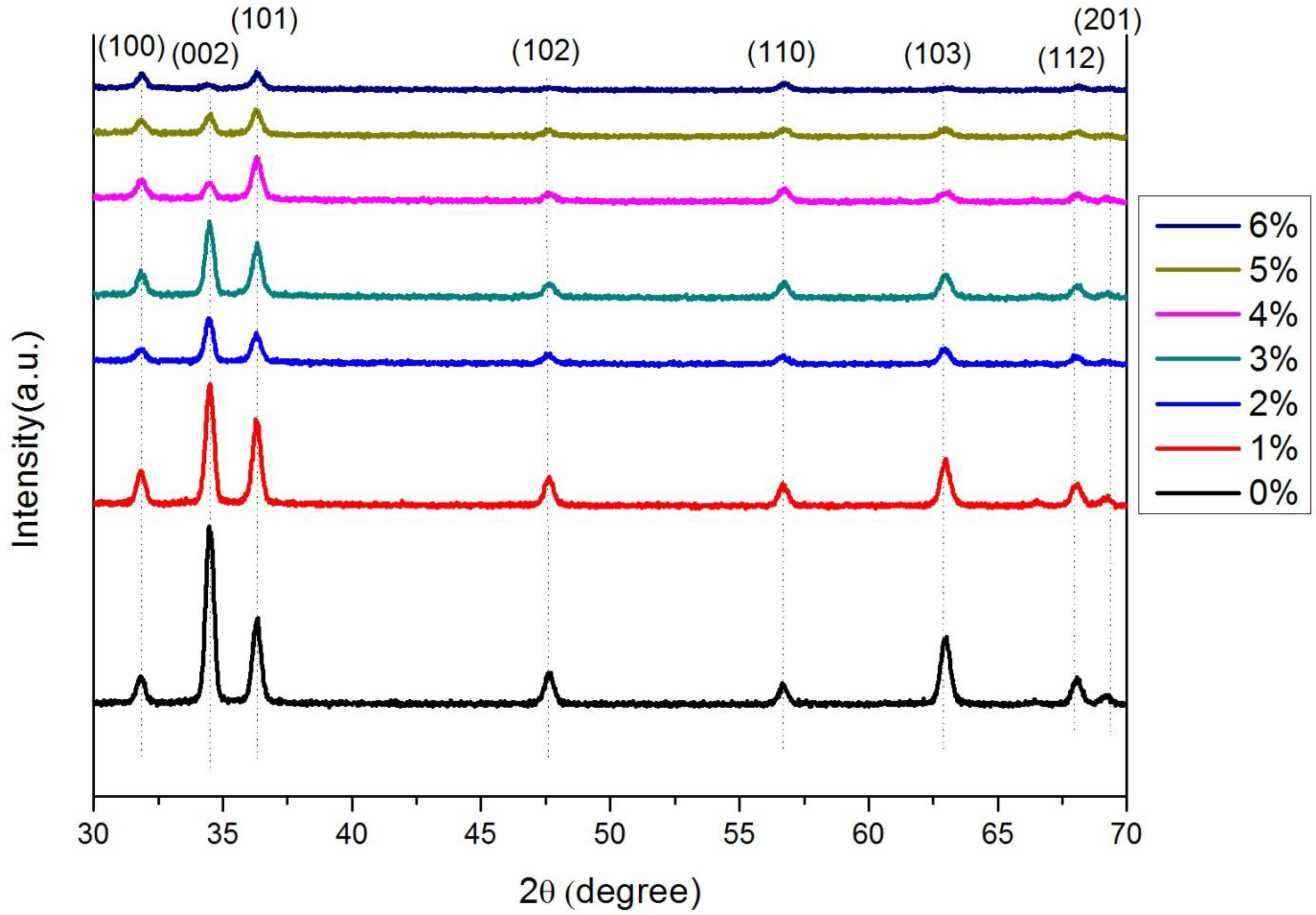
2.1. Morphological and Structural Properties

| Sample | Mobility (cm2/V·s) | Concentration (cm−3) | R0 (Ω·cm) | Conductivity |
|---|---|---|---|---|
| ZnO | 6.96 | 1.347 × 10¹⁷ | 6.66 | n |
| Cu0.03Zn0.97O | 1.06 | 2.599 × 10¹⁷ | 22.76 | n |
| Cu0.04Zn0.96O | 0.79 | 3.016 × 10¹⁸ | 2.619 | n |
| Cu0.05Zn0.95O | 0.692 | 5.517 × 10¹⁸ | 1.634 | p |

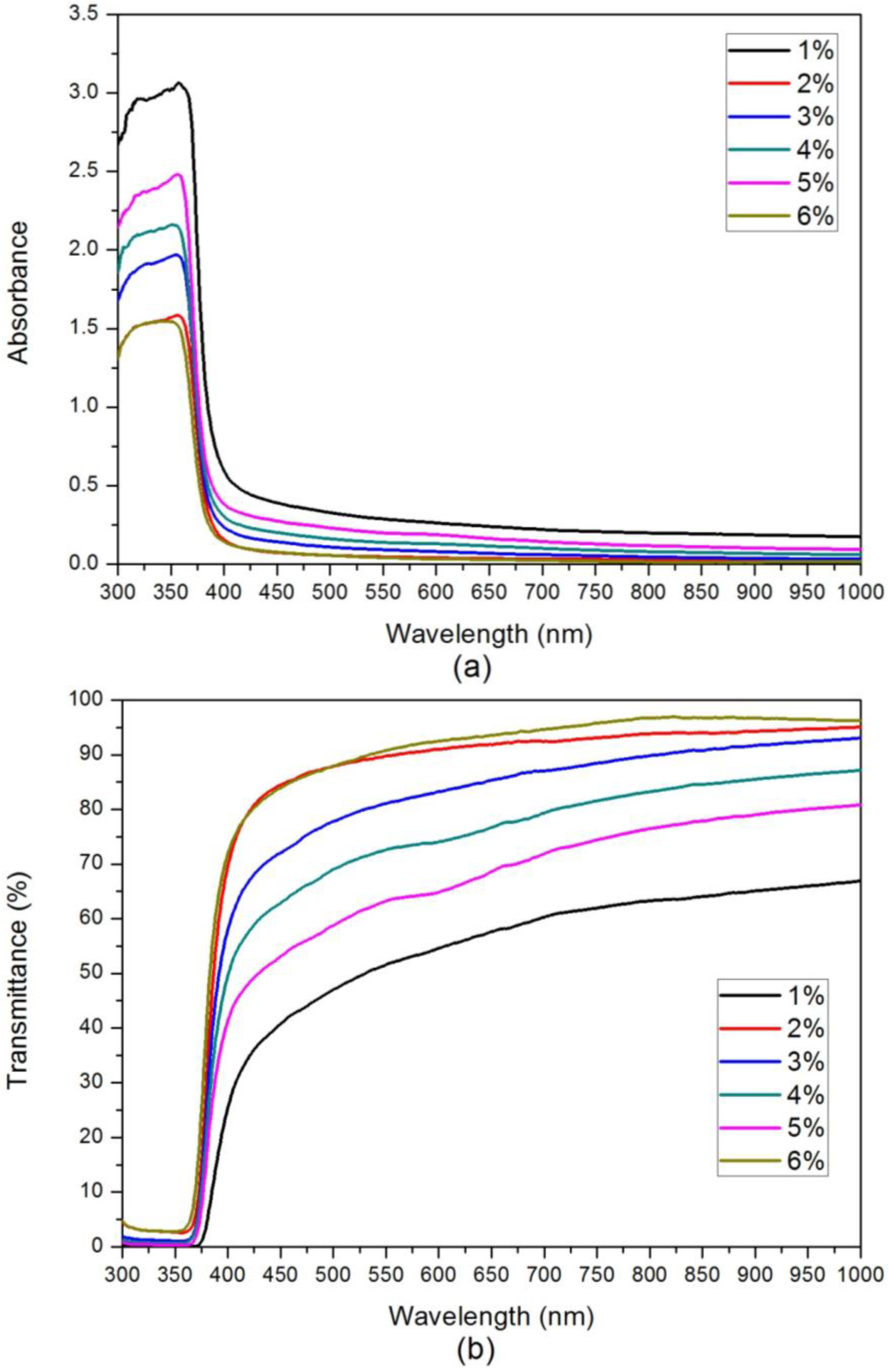
2.2. Transmission and Absorption

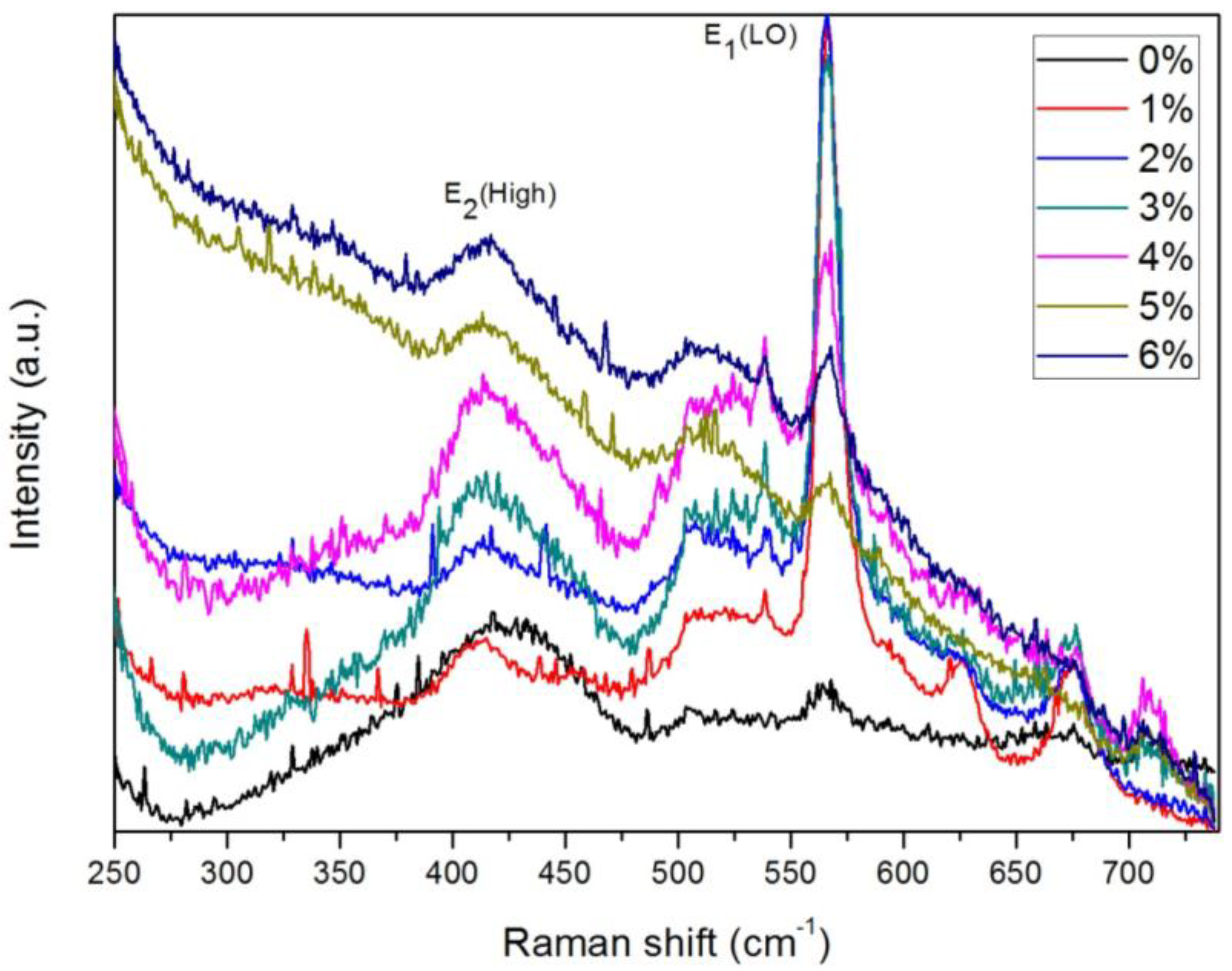
2.3. Raman Analysis

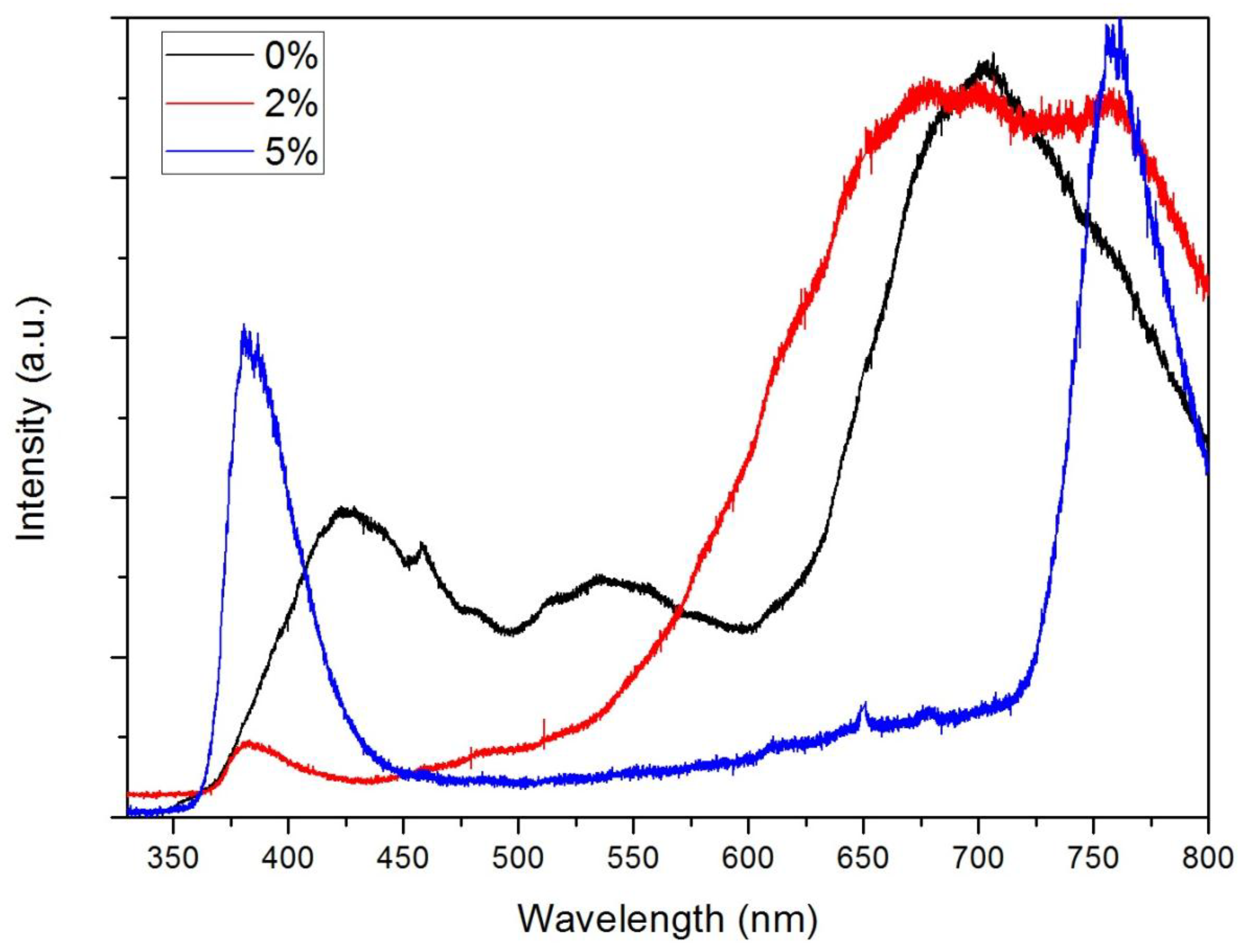
2.4. Photoluminescence
3. Experimental Section
4. Conclusions
Acknowledgments
Author Contributions
Conflicts of Interest
References
- Hsiao, C.S.; Chen, S.Y.; Kuo, W.L.; Lin, C.C.; Cheng, S.Y. Synthesis and optical properties of white-light-emitting alumina/ZnO nanotubes. Nanotechnology 2008, 19, 405608. [Google Scholar] [CrossRef] [PubMed]
- Look, D.C.; Claflin, B.; Alivov, Y.I.; Park, S.J. The future of ZnO light emitters. Phys. Status Solidi (a) 2004, 201, 2203–2212. [Google Scholar] [CrossRef]
- Pauporté, T.; Lincot, D.; Viana, B.; Pellé, F. Toward laser emission of epitaxial nanorod arrays of ZnO grown by electrodeposition. Appl. Phys. Lett. 2006, 89, 233112:1–233112:3. [Google Scholar] [CrossRef]
- Law, M.; Greene, L.E.; Johnson, J.C.; Saykally, R.; Yang, P. Nanowire dye-sensitized solar cells. Nat. Mater. 2005, 4, 455–459. [Google Scholar] [CrossRef] [PubMed]
- Aoumeur, F.Z.; Benkabou, K.H.; Belgoumène, B. Structural and dynamical properties of ZnO in zinc-blende and rocksalt phases. Phys. B Condens. Matter 2003, 337, 292–297. [Google Scholar] [CrossRef]
- Soudi, A.; Khan, E.H.; Dickinson, J.T.; Gu, Y. Observation of unintentionally incorporated nitrogen-related complexes in ZnO and GaN nanowires. Nano Lett. 2009, 9, 1844–1849. [Google Scholar] [CrossRef] [PubMed]
- Morkoç, H.; Strite, S.; Gao, G.B.; Lin, M.E.; Sverdlov, B.; Burns, M. Large-band-gap SiC, III-V nitride, and II-VI ZnSe-based semiconductor device technologies. J. Appl. Phys. 1994, 76, 1363–1398. [Google Scholar] [CrossRef]
- Bagnall, D.M.; Chen, Y.F.; Shen, M.Y.; Zhu, Z.; Goto, T.; Yao, T. Room temperature excitonic stimulated emission from zinc oxide epilayers grown by plasma-assisted MBE. J. Cryst. Growth 1998, 184–185, 605–609. [Google Scholar] [CrossRef]
- Ai, Z.; Wu, H.; Lin, Y.; Zhou, Z.; Wang, S.; Liu, C. Carrier concentration effect of Cu-doped ZnO films for room temperature ferromagnetism. Jpn. J. Appl. Phys. 2012, 51, 103003. [Google Scholar] [CrossRef]
- Aravind, A.; Jayaraj, M.K.; Kumar, M.; Chandra, R. Optical and magnetic properties of copper doped ZnO nanorods prepared by hydrothermal method. J. Mater. Sci. Mater. Electron. 2013, 24, 106–112. [Google Scholar] [CrossRef]
- Zhang, L.Q.; Ye, Z.Z.; Lu, J.G.; Lu, B.; Zhang, Y.Z.; Zhu, L.P.; Zhang, J.; Yang, D.; Wu, K.W.; Huang, J.; et al. Influence of p-type and n-type dopants on the magnetic properties of ZnCuO based diluted magnetic semiconductor thin films. J. Phys. D Appl. Phys. 2010, 43, 015001. [Google Scholar] [CrossRef]
- Chan, Y.-M.; Wu, Y.-T.; Jou, S. Oxide solar cells fabricated using zinc oxide and plasma-oxidized cuprous oxide. Jpn. J. Appl. Phys. 2012, 51, 125502. [Google Scholar] [CrossRef]
- Li, M.-H.; Chen, X.-M.; Xu, J.-P.; Zhang, X.-S.; Wu, Y.-Y.; Li, P.; Niu, X.-P.; Luo, C.-Y.; Li, L. Synthesis and photoluminescent properties of ZnO:Cu/ZnO core/shell nanocrystals. Optoelectron. Lett. 2012, 8, 241–244. [Google Scholar] [CrossRef]
- Xiong, Z.; Chen, L.; Zheng, C. Theoretical studies on p-type conduction in (S,Cu) co-doped ZnO. Adv. Mater. Res. 2011, 306, 269–273. [Google Scholar] [CrossRef]
- Liu, H.; Yang, J.; Hua, Z.; Zhang, Y.; Yang, L.; Xiao, L.; Xie, Z. The structure and magnetic properties of Cu-doped ZnO prepared by sol-gel method. Appl. Surf. Sci. 2010, 256, 4162–4165. [Google Scholar] [CrossRef]
- Sato, K.; Katayama-Yoshida, H. Ab initio study on the magnetism in ZnO-, ZnS-, ZnSe- and ZnTe-based diluted magnetic semiconductors. Phys. Status Solidi B 2002, 229, 673–680. [Google Scholar] [CrossRef]
- Lee, S.; Shon, Y.; Lee, S.-W.; Hwang, S.J.; Lee, H.S.; Kang, T.W.; Kim, D.Y. Improved ferromagnetism of (Zn0.93 Mn0.07) O through rapid thermal annealing. Appl. Phys. Lett. 2006, 88, 212513:1–212513:3. [Google Scholar]
- Janisch, R.; Gopal, P.; Spaldin, N.A. Transition metal-doped TiO2 and ZnO—Present status of the field. J. Phys. Condens. Matter 2005, 17, 657–689. [Google Scholar] [CrossRef]
- Gopal, P.; Spaldin, N.A. Magnetic interactions in transition-metal-doped ZnO: An ab initio study. Phys. Rev. B 2006, 74, 094418. [Google Scholar] [CrossRef]
- Zheng, Y.; Boulliard, J.C.; Demaille, D.; Bernard, Y.; Pétroff, J.F. Study of ZnO crystals and Zn1−xMxO (M=Co, Mn) epilayers grown by pulsed laser deposition on ZnO(001) substrate. J. Cryst. Growth 2005, 274, 156–166. [Google Scholar] [CrossRef]
- Polyakov, A.Y.; Govorkov, A.V.; Smirnov, N.B.; Pashkova, N.V.; Pearton, S.J.; Ip, K.; Frazier, R.M.; Abernathy, C.R.; Norton, D.P.; Zavada, J.M.; et al. Optical and magnetic properties of ZnO bulk crystals implanted with Cr and Fe. Mater. Sci. Semicond. Process. 2004, 7, 77–81. [Google Scholar] [CrossRef]
- Dietl, T.; Ohno, H.; Matsukura, F.; Cibert, J.; Ferrand, D. Zener model description of ferromagnetism in zinc-blende magnetic semiconductors. Science 2000, 287, 1019–1022. [Google Scholar] [CrossRef] [PubMed]
- Kim, C.O.; Kim, S.; Oh, H.T.; Choi, S.-H.; Shon, Y.; Lee, S.; Hwang, H.N.; Hwang, C.-C. Effect of electrical conduction properties on magnetic behaviors of Cu-doped ZnO thin films. Phys. B Condens. Matter 2010, 405, 4678–4681. [Google Scholar] [CrossRef]
- Zheng, J.H.; Song, J.L.; Li, X.J.; Jiang, Q.; Lian, J.S. Experimental and first-principle investigation of Cu-doped ZnO ferromagnetic powders. Cryst. Res. Technol. 2011, 46, 1143–1148. [Google Scholar] [CrossRef]
- Shannon, R.D. Revised effective ionic radii and systematic studies of interatomic distances in halides and chalcogenides. Acta Crystallogr. Sect. A 1976, 32, 751–767. [Google Scholar] [CrossRef]
- Keis, K.; Vayssieres, L.; Rensmo, H.; Lindquist, S.-E.; Hagfeldt, A. Photoelectrochemical properties of Nano- to microstructured ZnO electrodes. J. Electrochem. Soc. 2001, 148, 149–155. [Google Scholar] [CrossRef]
- Jeong, T.S.; Han, M.S.; Youn, C.J.; Park, Y.S. Raman scattering and photoluminescence of As ion-implanted ZnO single crystal. J. Appl. Phys. 2004, 96, 175–179. [Google Scholar] [CrossRef]
- Samanta, K.; Bhattacharya, P.; Katiyar, R.S.; Iwamoto, W.; Pagliuso, P.G.; Rettori, C. Raman scattering studies in dilute magnetic semiconductor Zn1−xCoxO. Phys. Rev. B 2006, 73, 245213. [Google Scholar] [CrossRef]
- Sharma, P.K.; Dutta, R.K.; Pandey, A.C. Doping dependent room-temperature ferromagnetism and structural properties of dilute magnetic semiconductor ZnO:Cu2+ nanorods. J. Magn. Magn. Mater. 2009, 321, 4001–4005. [Google Scholar] [CrossRef]
- Alim, K.A.; Fonoberov, V.A.; Balandin, A.A. Origin of the optical phonon frequency shifts in ZnO quantum dots. Appl. Phys. Lett. 2005, 86, 053103:1–053103:3. [Google Scholar] [CrossRef]
- Pradhan, A.K.; Zhang, K.; Loutts, G.B.; Roy, U.N.; Cui, Y.; Burger, A. Structural and spectroscopic characteristics of ZnO and ZnO:Er3+ nanostructures. J. Phys. Condens. Matter 2004, 16, 7123–7129. [Google Scholar] [CrossRef]
- Cuscó, R.; Alarcón-Lladó, E.; Ibáñez, J.; Artús, L.; Jiménez, J.; Wang, B.; Callahan, M.J. Temperature dependence of Raman scattering in ZnO. Phys. Rev. B 2007, 75, 165202. [Google Scholar] [CrossRef]
- Wang, H.; Wang, H.B.; Yang, F.J.; Chen, Y.; Zhang, C.; Yang, C.P.; Li, Q.; Wong, S.P. Structure and magnetic properties of Zn1−xCoxO single-crystalline nanorods synthesized by a wet chemical method. Nanotechnology 2006, 17. [Google Scholar] [CrossRef] [PubMed]
- Xu, C.X.; Sun, X.W.; Zhang, X.H.; Ke, L.; Chua, S.J. Photoluminescent properties of copper-doped zinc oxide nanowires. Nanotechnology 2004, 15, 856–861. [Google Scholar] [CrossRef]
- Fan, H.J.; Scholz, R.; Kolb, F.M.; Zacharias, M.; Gösele, U.; Heyroth, F.; Eisenschmidt, C.; Hempel, T.; Christen, J. On the growth mechanism and optical properties of ZnO multi-layer nanosheets. Appl. Phys. A 2004, 79, 1895–1900. [Google Scholar] [CrossRef]
- Lupan, O.; Pauporté, T.; Viana, B.; Tiginyanu, I.M.; Ursaki, V.V.; Cortès, R. Epitaxial electrodeposition of ZnO nanowire arrays on p-GaN for efficient UV-light-emitting diode fabrication. ACS Appl. Mater Interfaces 2010, 2, 2083–2090. [Google Scholar] [CrossRef]
- Wang, X.B.; Song, C.; Geng, K.W.; Zeng, F.; Pan, F. Photoluminescence and Raman scattering of Cu-doped ZnO films prepared by magnetron sputtering. Appl. Surf. Sci. 2007, 253, 6905–6909. [Google Scholar] [CrossRef]
© 2014 by the authors; licensee MDPI, Basel, Switzerland. This article is an open access article distributed under the terms and conditions of the Creative Commons Attribution license (http://creativecommons.org/licenses/by/4.0/).
Share and Cite
Chen, L.-C.; Hsieh, C.-A.; Zhang, X. Electrical Properties of CZO Films Prepared by Ultrasonic Spray Pyrolysis. Materials 2014, 7, 7304-7313. https://doi.org/10.3390/ma7117304
Chen L-C, Hsieh C-A, Zhang X. Electrical Properties of CZO Films Prepared by Ultrasonic Spray Pyrolysis. Materials. 2014; 7(11):7304-7313. https://doi.org/10.3390/ma7117304
Chicago/Turabian StyleChen, Lung-Chien, Cheng-An Hsieh, and Xiuyu Zhang. 2014. "Electrical Properties of CZO Films Prepared by Ultrasonic Spray Pyrolysis" Materials 7, no. 11: 7304-7313. https://doi.org/10.3390/ma7117304
APA StyleChen, L.-C., Hsieh, C.-A., & Zhang, X. (2014). Electrical Properties of CZO Films Prepared by Ultrasonic Spray Pyrolysis. Materials, 7(11), 7304-7313. https://doi.org/10.3390/ma7117304