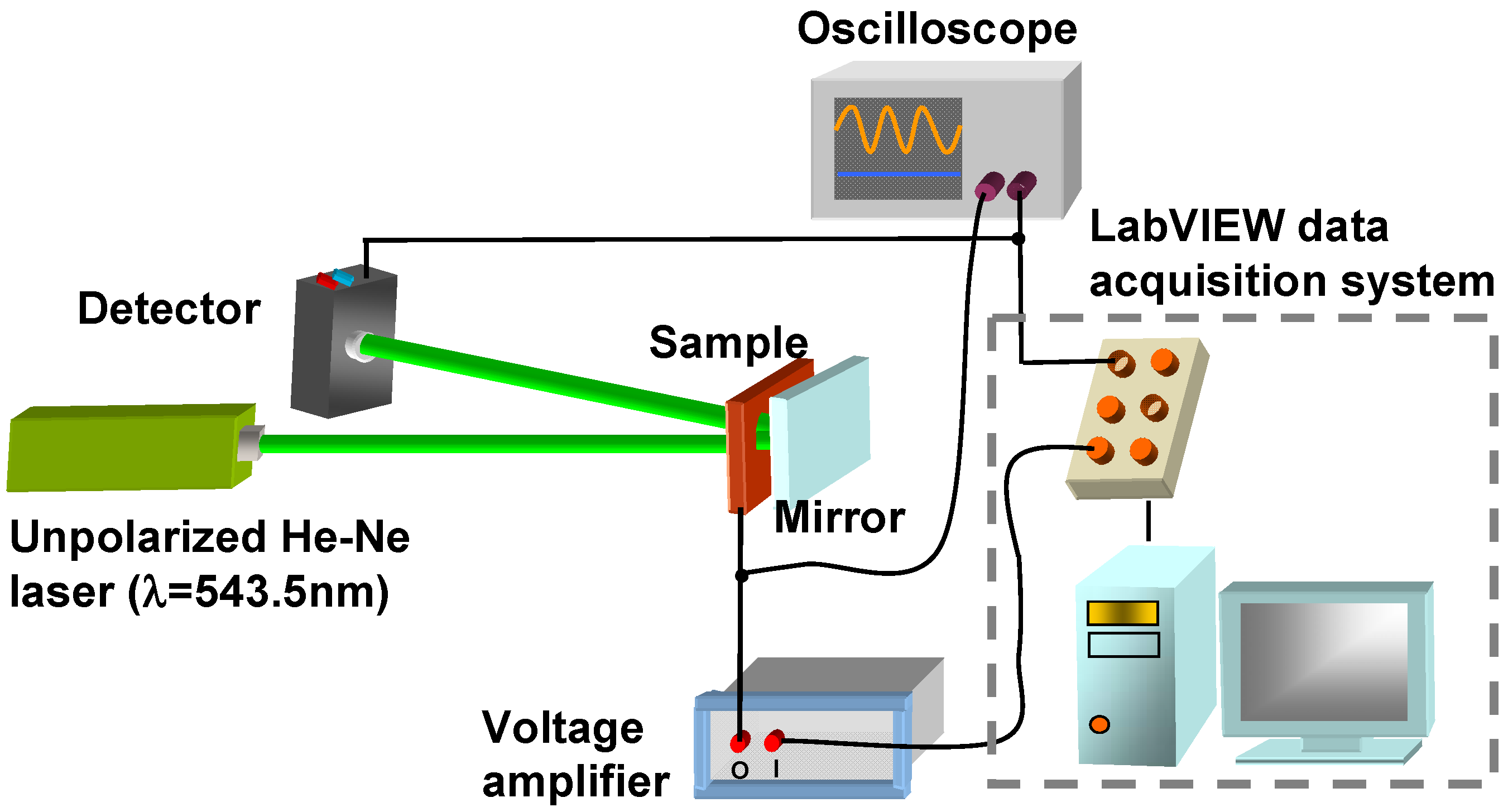
In order to measure the electro-optical properties of dye-doped LC gels, we adopted the typical reflectance measurement setup shown in
Figure 3. We used an unpolarized green He-Ne laser (λ = 543.5 nm, Melles Griot, Model 05-LGR-173) as the incident light source. The light double passes through the cell by putting a dielectric-reflected mirror behind the sample and the corresponding collection angle is around 5°. We measured the reflectance with a large area photodiode detector (New Focus, Model 2031) which was placed ~23 cm behind the sample. The distance between the detector and the sample is larger; the measuring reflectance is smaller because of the scattering effect. The reflectance is normalized to that of a pure LC cell with the same cell gaps. The Labview data acquisition system was used to applied voltages and collect light intensity at the same time. The response time was measured by an oscilloscope. In the following sections four effects are discussed including the effects of the curing temperature, the UV curing intensity, the monomer concentration, and the cell gap.
3.1. Effect of Curing Temperature
We summarize the effect of curing temperature in this section since we have previously discussed this topic [
8,
11].
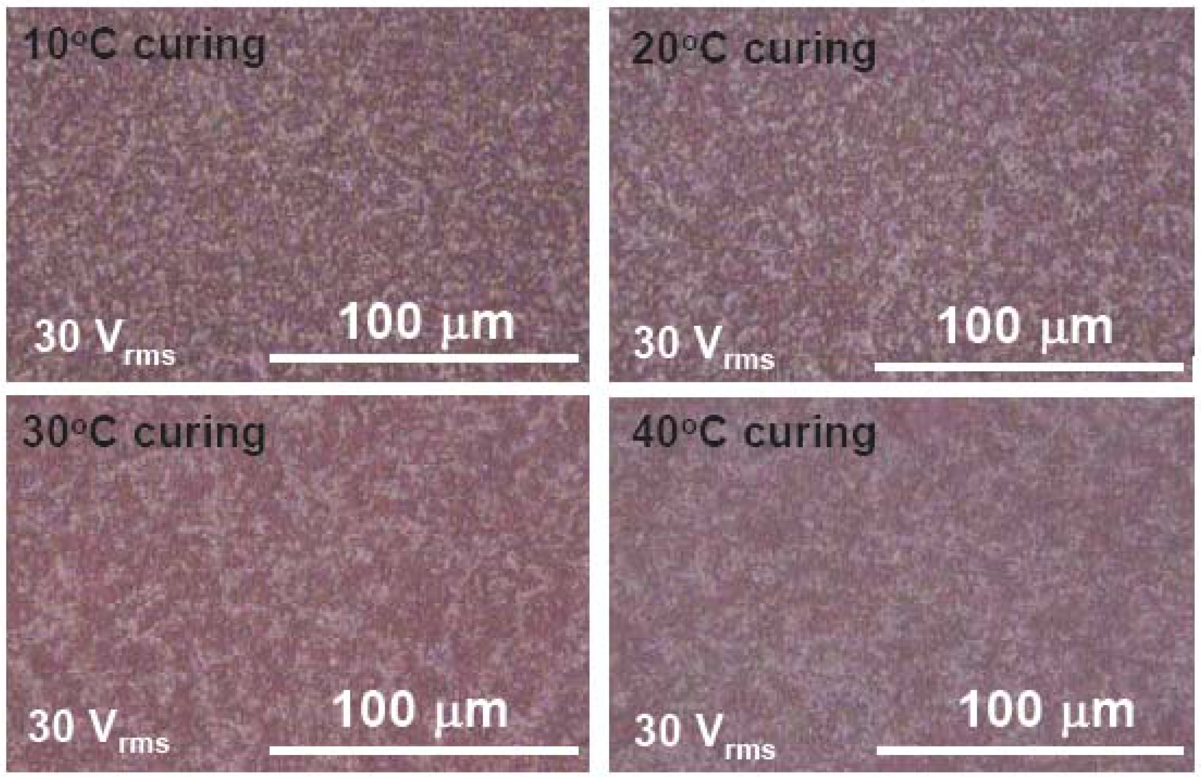
Figure 4 shows the morphologies observed under a microscope at 30 V
rms and different curing temperatures.
Figure 4.
The microscopic images of dye-doped LC gels with various curing temperature. The applied voltage is 30 Vrms.
Figure 4.
The microscopic images of dye-doped LC gels with various curing temperature. The applied voltage is 30 Vrms.
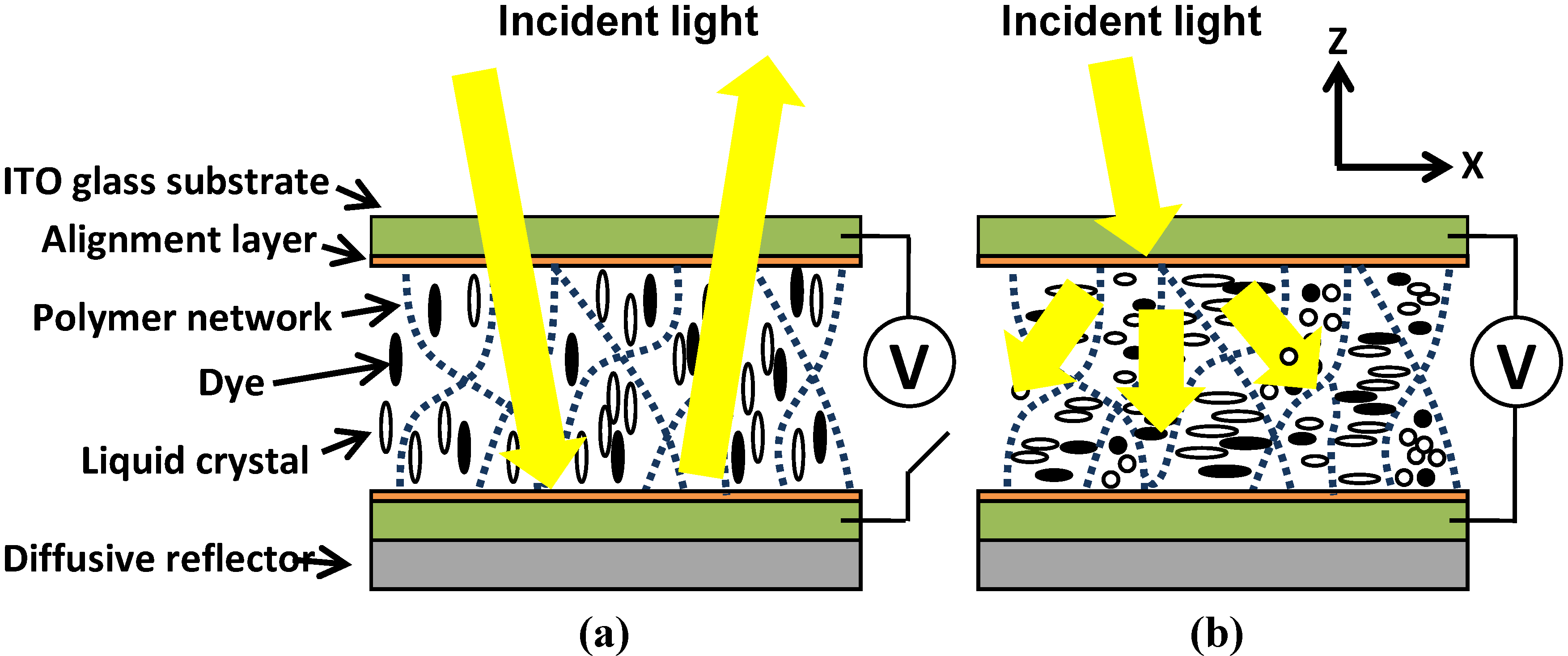
At V = 0, the cell shows a bright state because of the vertically aligned polymer networks, LC and dye molecules. At 30 V
rms, it shows the fine domain textures of the polymer networks, and appears red because of dye molecules, as shown in
Figure 4. The higher curing temperature, the larger the domain size of dye-doped LC gels. The domain size affects the electro-optical properties of dye-doped LC gels. The LC molecules are easily rotated by the applied voltage as a weak anchoring energy; therefore, dye-doped LC gels have a lower threshold voltage and a slower decay time with larger domain sizes. The threshold voltage is the voltage at which the reflectance starts to decrease. The threshold voltage decreases from 5.82 (10 °C) to 3.72 V
rms (40 °C) and decay time increases from 6 ms (10 °C) to 22.7 ms (40 °C). The reflectance at V=0 decreases from 55% (10 °C) to 42% (40 °C) with the increases of the curing temperature. That is because the better vertical alignment of LC directors, dye molecules and polymer networks at smaller domain size. The raising times are all around 0.4 ms at different curing temperature. The contrast ratio, a reflectance ratio of 0 V to 30 V
rms, is ~450:1 at 10 °C, 250:1 at 20 °C, 200:1 at 30 °C, and 300:1 at 40 °C. The contrast ratio decreases at T < 30 °C due to the larger polydomain and then increases as T > 30 °C caused by the dynamic scattering, a fluctuation of liquid crystal directors in polymer domains, which help decreasing the dark state reflectance. The reason why the larger domain has the dynamic scattering is still unclear.
Figure 5.
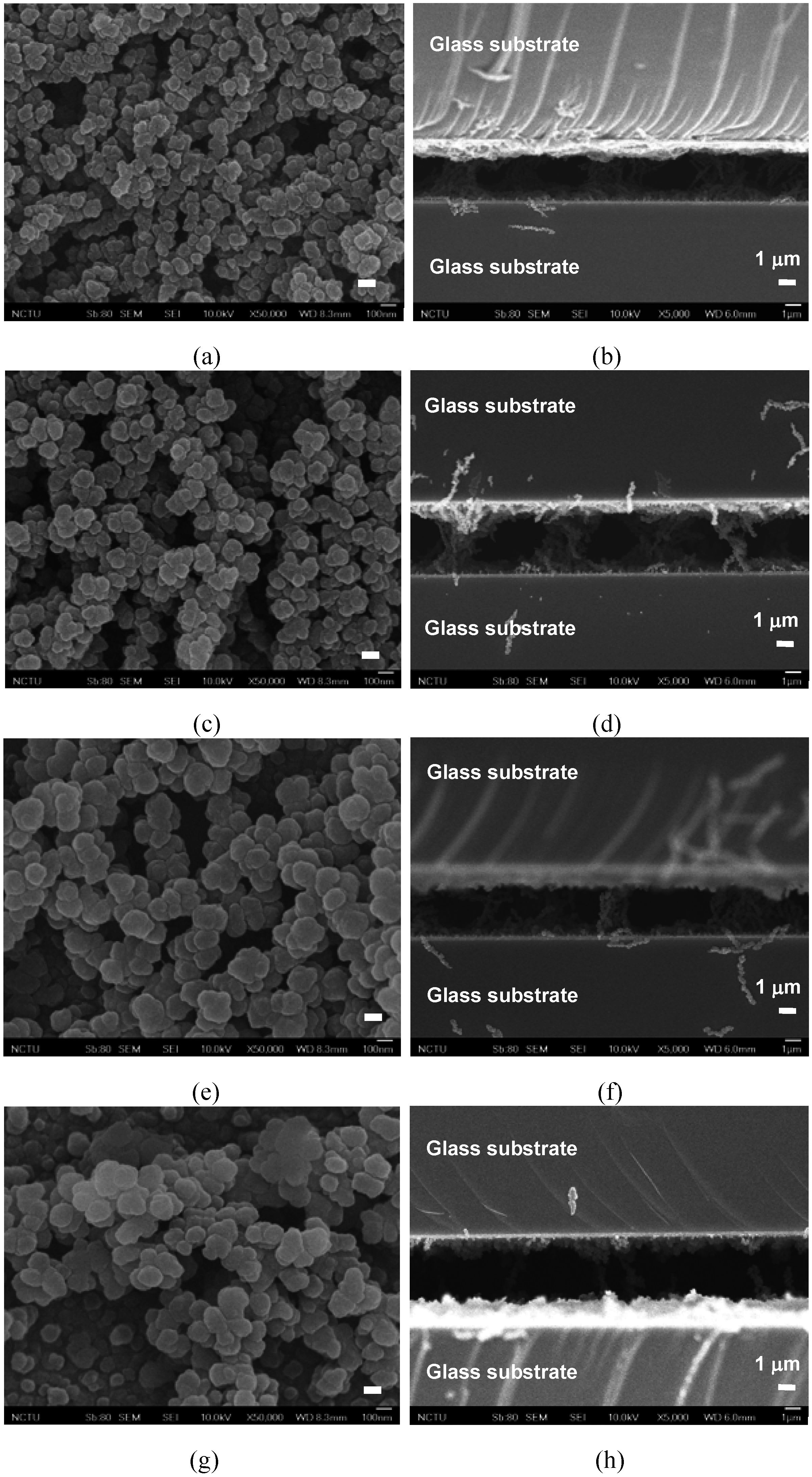
SEM photographs of dye-doped LC gels at curing temperatures 10 °C (a, b), 20 °C (c, d), 30 °C (e, f), and 40 °C (g, h). The LC and dye were extracted. (a), (c), (e) and (g) are the top views of the cells. (b), (d), (f), and (h) are the side views of the cells. The white-indicated bars in (a), (c), (e) and (g) are 100 nm.
Scanning Electron Microscopy (SEM) photographs after removing LC and dye molecules with hexane are shown in
Figure 5(a)-(h).
Figure 5(a),
Figure 5(c),
Figure 5(e) and
Figure 5(g) are the top views of the cells at different curing temperatures (T).
Figure 5(b),
Figure 5(d),
Figure 5(f), and (
Figure 5h) are the side views of the cells at different curing temperatures. In
Figure 5(b),
Figure 5(d),
Figure 5(f), and
Figure 5(h), the polymer networks are perpendicular to the glass substrates. The polymer networks of dye-doped LC gels consist of chain-linked polymer grains. The averaged sizes of polymer grains measured from
Figure 5(a),
Figure 5(c),
Figure 5(e) and
Figure 5(g) are around 68 nm at T = 10 °C, 94 nm at T = 20 °C, 125 nm at T = 30 °C, and 132 nm at T = 40 °C. The averaged domain sizes of polymer networks measured from
Figure 5(b),
Figure 5(d),
Figure 5(f), and
Figure 5(h) are around 3.25 μm at T = 10 °C, 4.62 μm at T = 20 °C, 4.78 μm at T = 30 °C, 6.12 μm at T = 40 °C. Both of the domain sizes and the size of polymer grains increase with curing temperatures. The scattering is mainly because of the domain sizes of polymer networks are near wavelength of incident light while the sizes of polymer grains are smaller than the wavelength.
3.2. Effect of UV Curing Intensity
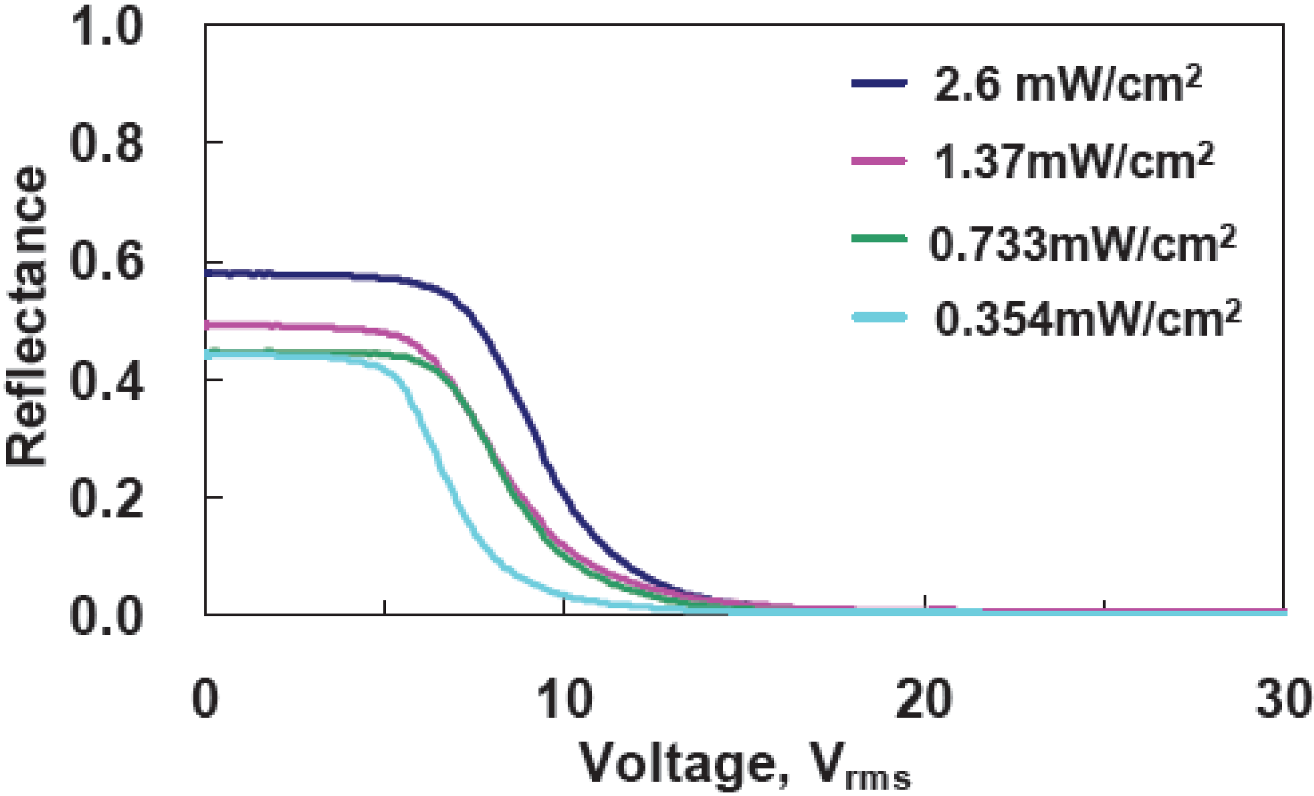
To examine the effect of UV curing intensity (I), we prepared four samples with the same mixtures at the curing temperature 10 °C, but at different UV curing intensities, which were 2.6, 1.37, 0.733, 0.354 mW/cm
2. The cell gaps were 5 μm. The reflectance as a function of a voltage is shown in
Figure 6. With the increases of UV curing intensity, threshold voltage (V
th) increases from 4.82 V
rms (I ~ 0.354 mW/cm
2) to 5.92 V
rms (I~2.6 mW/cm
2 ). The reflectance at V = 0 increases from 44% (I ~ 0.354 mW/cm
2 ) to ~57% ( I~2.6 mW/cm
2). In
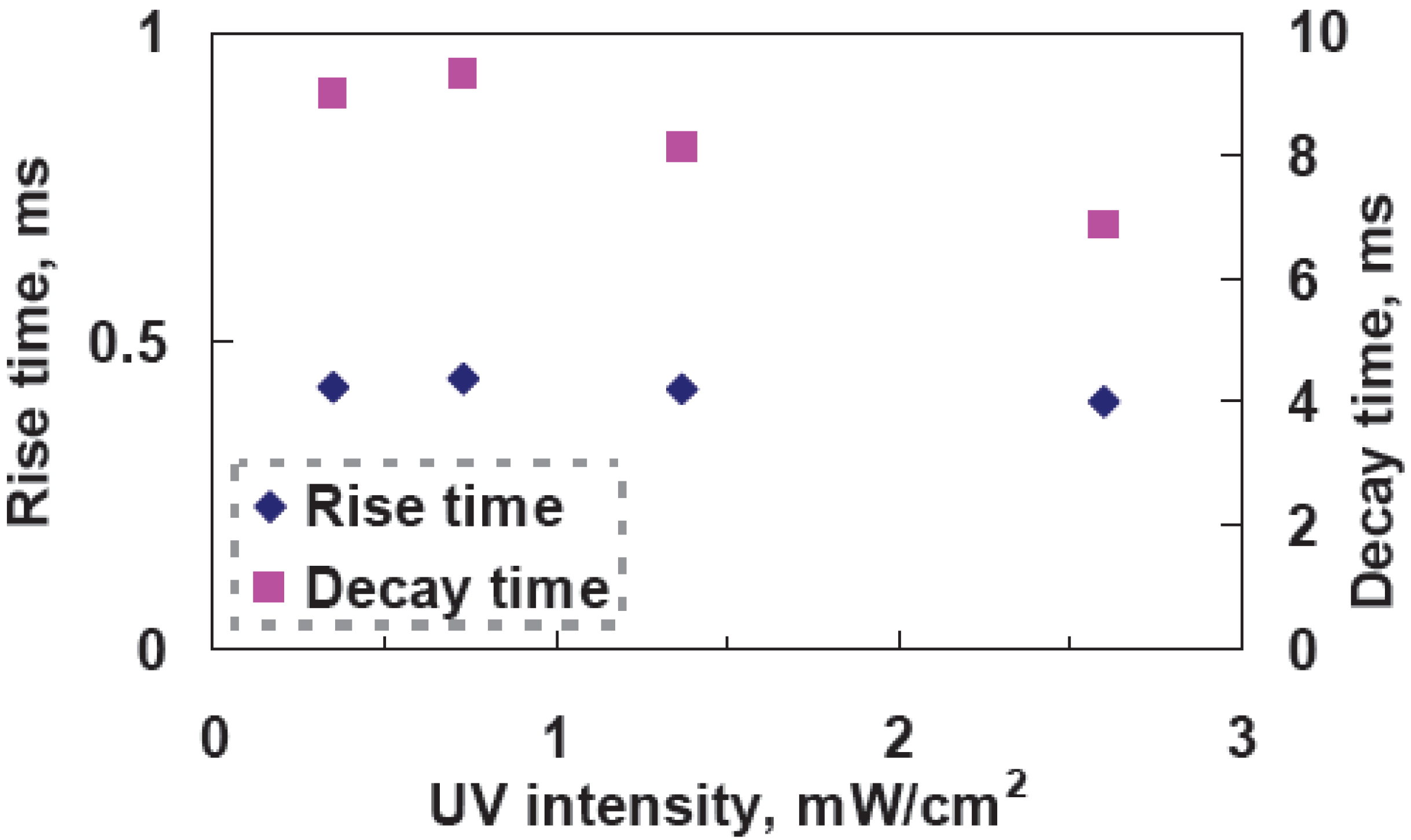
Figure 7, rise time is around 0.4 ms, but decay time decreases from 9 ms (I ~ 0.354 mW/cm
2) to 6.88 ms (I ~ 2.6 mW/cm
2). The larger UV curing intensity results in smaller domain size of polymer networks. That causes the stronger anchoring energy and then enlarges the threshold voltage and boost the response time. The reflectance at V = 0 decreases under higher UV curing intensity owing to better vertically alignment at V = 0.
Figure 6.
Voltage-dependent reflectance at various curing intensities at a curing temperature of 10 °C.
Figure 6.
Voltage-dependent reflectance at various curing intensities at a curing temperature of 10 °C.
Figure 7.
Measured response time as a function of UV curing intensity at a curing temperature of 10 °C.
Figure 7.
Measured response time as a function of UV curing intensity at a curing temperature of 10 °C.
3.4. Cell Gap Effect
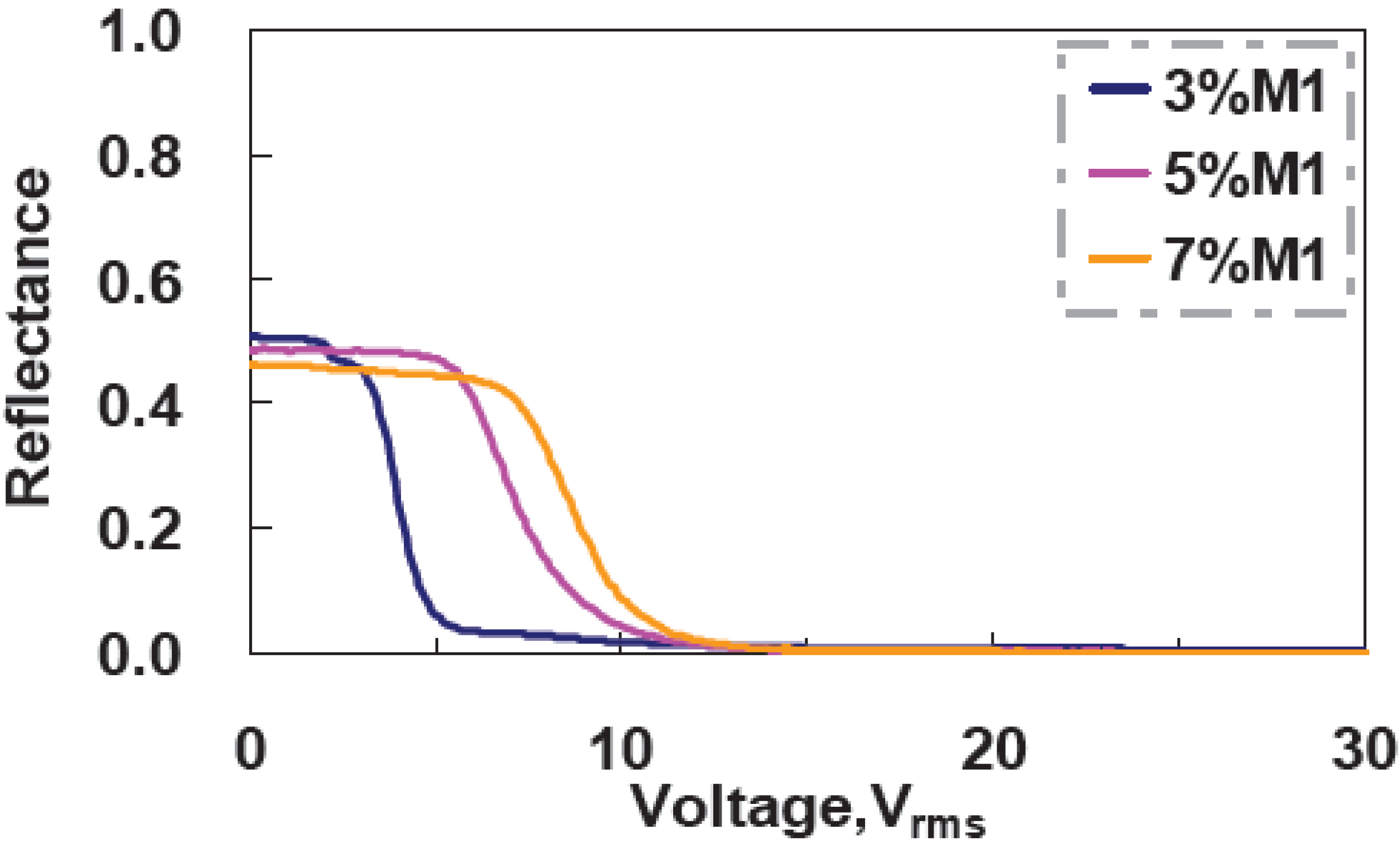
The threshold voltage increases from 2.1 V
rms (at 3 wt% M1) to 6.52 V
rms (at 7 wt% M1) with the monomer concentration due to the denser polymer networks. The reflectance at V = 0 decrease slightly (from 51% at 3 wt% M1 to 46% at 7 wt% M1). That is because denser polymer networks affect the vertical alignment of LC directors and also increase the scattering. CR increases from 222:1 (at 3 wt% M1) to 486:1 (at 7 wt% M1) owning to better scattering of higher monomer concentration at the high driving voltage.
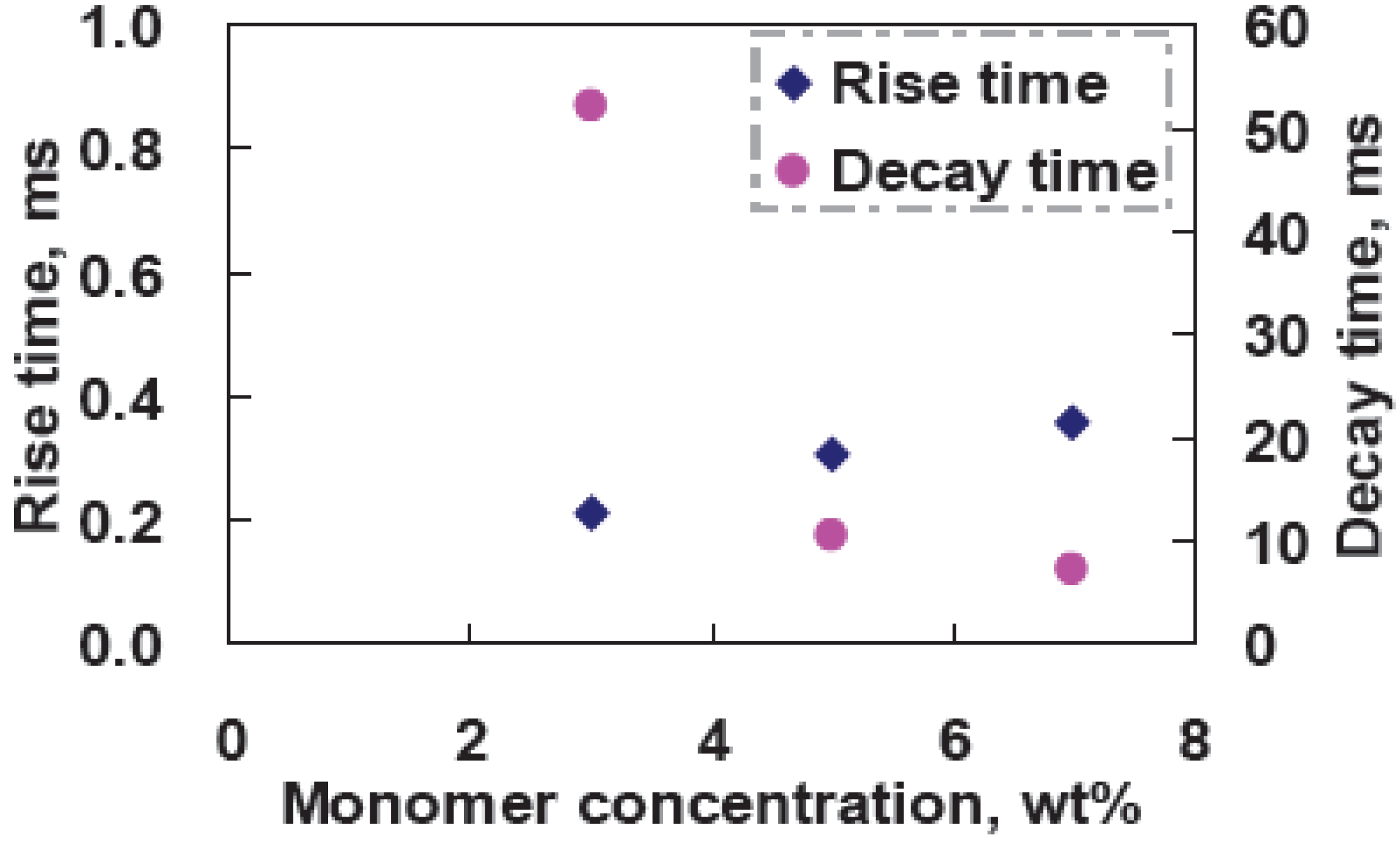
Figure 9 shows the measured response time as a function of UV curing intensity. Rise time is around 0.2 ms-0.4 ms, and decay time increases from 52 ms (at 3 wt% M1) to 7.3 ms (at 7 wt%M1). The higher monomer concentration has higher anchoring energy of polymer networks; therefore, the LC directors are relaxed back faster after turning off the applied voltage [
12].
Figure 9.
Measured response time as a function of monomer concentration.
Figure 9.
Measured response time as a function of monomer concentration.
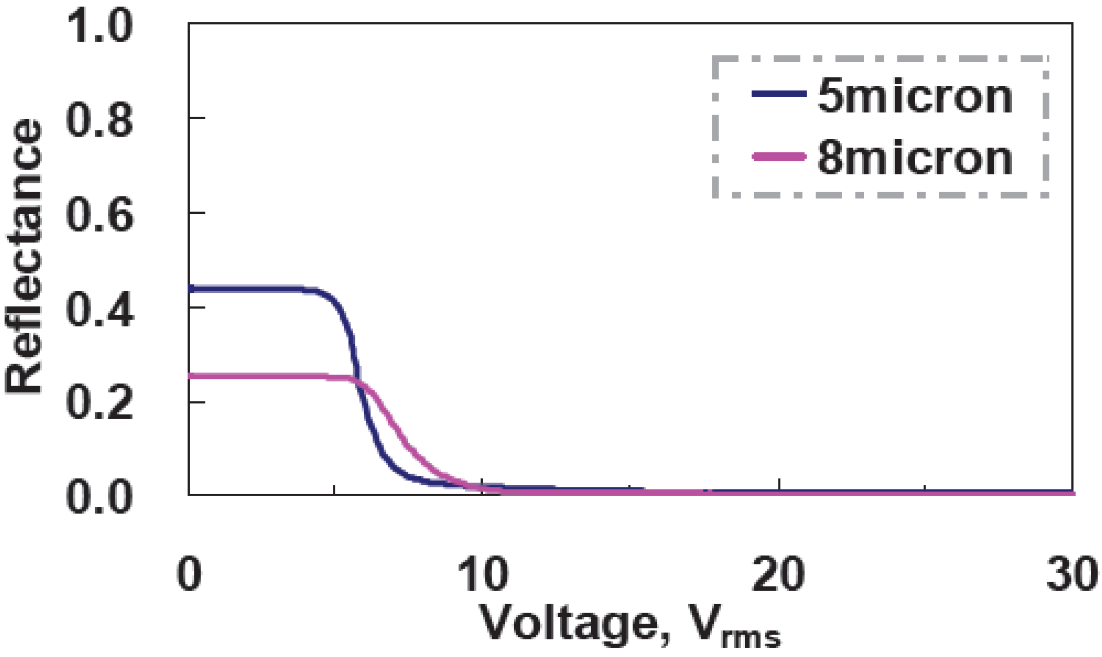
We can also increase the cell gap in order to enlarge the scattering and absorption of incident light. Two samples with a mixture of ZLI4788, M1, and S428 at 90:5:5 wt% ratios are made under the same curing condition:curing temperature ~30 °C and UV curing intensity ~2.6 mW/cm
2. The cell gaps of two samples are 5 μm and 8 μm. As one can see in
Figure 10, the reflectance at V=0 drops from 44% for 5 μm cell gap to 25% for an 8 μm cell gap, even though CR increases from 208:1 to 264:1 due to the better dark state in the larger cell gap. The large cell gap can help scattering and absorption; however, the trade off is low bright sate, the reflectance at V=0. Therefore, it is not worth increasing the cell gap.
Figure 10.
Voltage-dependent reflectance of different cell gaps.
Figure 10.
Voltage-dependent reflectance of different cell gaps.

