

Simulating Model Dielectric Functions of Dilute GaAs1-xNx in the Far-Infrared to Ultraviolet Wavelength Regimes



Abstract
1. Introduction
2. Background
2.1. Basic Properties of Dilute III-V-Ns
2.2. Structural and Phonon Characteristics
3. Theoretical Section
3.1. Lattice Dynamics
Rigid-Ion Model
3.2. Analyses of FTIR Spectra
3.2.1. Dielectric Response Function at
3.2.2. Dielectric Response Function at
3.3. Analyzing Spectroscopic Ellipsometry Data
Modified Adachi’s Model Dielectric Function
4. Numerical Computations: Results and Discussion
4.1. Phonon Dispersions
4.2. Local Vibrational Modes
4.2.1. Perturbation Matrix
4.2.2. Local Distortions of Isolated Defects
4.2.3. Impurity Modes
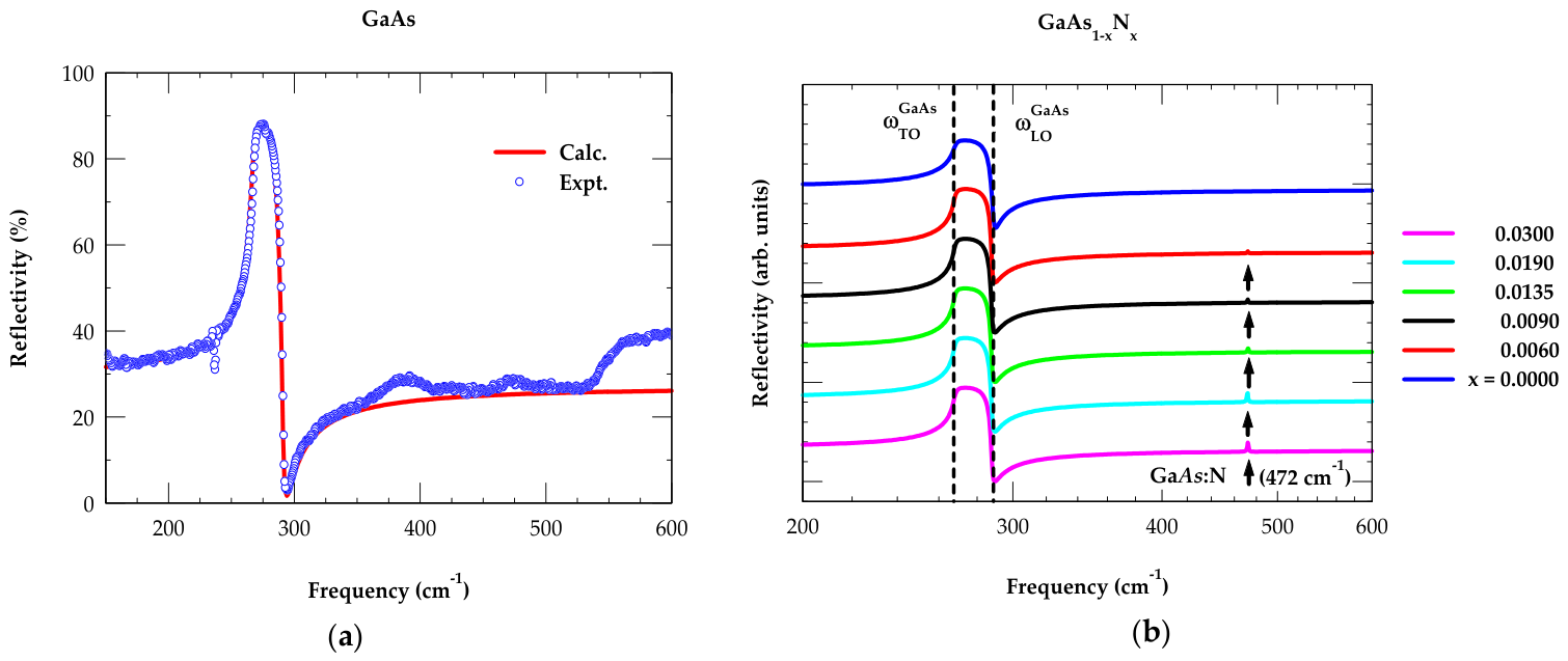
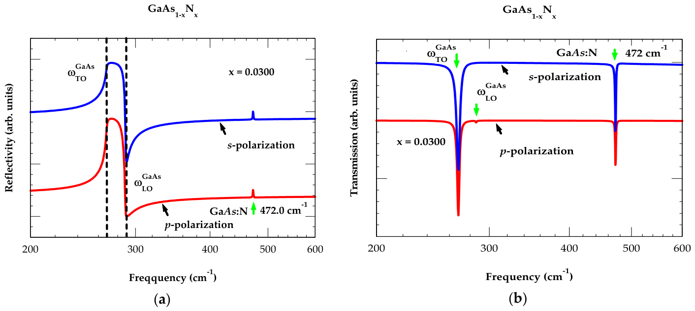
4.3. Reflectivity and Transmission Spectra
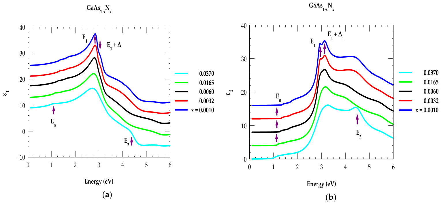
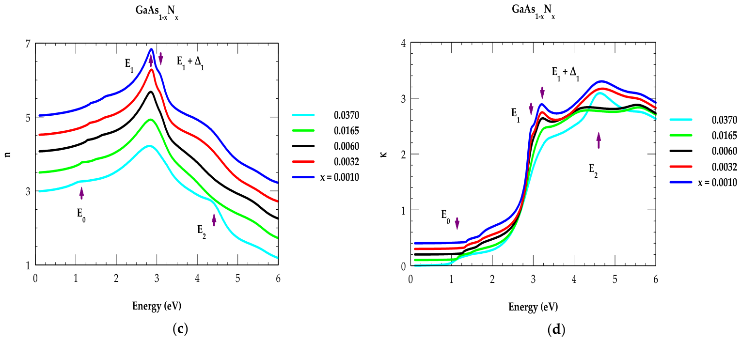
4.4. Optical Constants in the UV Region


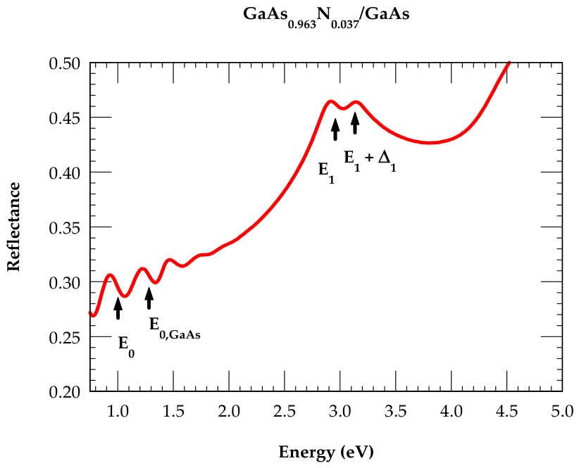
Reflectance of GaAs1-xNx/GaAs Epifilms
5. Concluding Remarks
Author Contributions
Funding
Data Availability Statement
Acknowledgments
Conflicts of Interest
References
- Dutta, P.S. Bulk Crystal Growth of Ternary III–V Semiconductors. In Springer Handbook of Crystal Growth; Springer: Berlin/Heidelberg, Germany, 2010; pp. 281–325. [Google Scholar] [CrossRef]
- Dutta, P.S. III–V Ternary bulk substrate growth technology: A review. J. Cryst. Growth 2005, 275, 106–112. [Google Scholar] [CrossRef]
- Prete, P.; Lovergine, N. High efficiency III–V nanowire solar cells: The road ahead. Nano Futur. 2025, 9, 042502. [Google Scholar] [CrossRef]
- Prete, P.; Lovergine, N. Dilute nitride III–V nanowires for high-efficiency intermediate-band photovoltaic cells: Materials requirements, self-assembly methods and properties. Prog. Cryst. Growth Charact. Mater. 2020, 66, 100510. [Google Scholar] [CrossRef]
- Bachmann, K.J.; Thiel, F.A.; Schreiber, H., Jr. Melt and solution growth of bulk single crystals of quaternary III–V alloys. Prog. Cryst. Growth Charact. 1979, 2, 171–206. [Google Scholar] [CrossRef]
- Swaminathan, V.; Macrander, A.T. Materials Aspects of GaAs and InP Based Structures; Prentice Hall: Hoboken, NJ, USA, 1991. [Google Scholar]
- Neuberger, M. III–V ternary semiconducting compounds-data tables. In Handbook of Electronic Materials; IFI/Plenum: New York, NY, USA, 1972; Volume 7. [Google Scholar]
- Madelung, O.; Schulz, M. (Eds.) Landolt–Börnstein, numerical data and functional relationships. In Science and Technology, Semiconductors; Springer: New York, NY, USA, 1987; Volume 22. [Google Scholar]
- Vurgaftman, I.; Meyer, J.R.; Ram-Mohan, L.R. Band parameters for III–V compound semiconductors and their alloys. J. Appl. Phys. 2001, 89, 5815–5875. [Google Scholar] [CrossRef]
- Nakajima, K.; Kusunoki, T.; Takenaka, C. Growth of ternary InxGa1−xAs bulk crystals with a uniform composition through supply of GaAs. J. Cryst. Growth 1991, 113, 485–490. [Google Scholar] [CrossRef]
- Lang, J.; Laurent, Y.; Maunaye, M.; Marchand, R. Nitrides—Structures and crystal growth. Prog. Cryst. Growth Charact. 1979, 2, 207–225. [Google Scholar] [CrossRef]
- Urakami, N.; Yamane, K.; Sekiguchi, H.; Okada, H.; Wakahar, A. Molecular-beam epitaxy growth of dilute GaAsN alloys by surface nitridation. J. Cryst. Growth 2016, 435, 19–23. [Google Scholar] [CrossRef]
- Dhar, S.; Halder, N.; Mondal, A. Investigation of deep level traps in dilute GaAsN layers grown by liquid phase epitaxy. Thin Solid Film. 2007, 515, 4427–4429. [Google Scholar] [CrossRef]
- Milanova, M.; Koleva, G.; Kakanakov, R.; Vitanov, P.K.; Alexieva, Z.; Goranova, E.A.; Arnaudov, B.; Evtimova, S.; Barthou, C.; Clerjaud, B. Dilute GaAsN and GaInAsN grown by liquid phase epitaxy. J. Phys. Conf. Ser. 2010, 223, 012016. [Google Scholar] [CrossRef]
- Milanova, M.; Koleva, G.; Kakanakov, R.; Vitanov, P.; Goranova, E.; Arnaudov, B.; Evtimova, S.; Barthou, C.; Clerjaud, B. Investigation of melt-grown dilute GaAsN and GaInAsN nanostructures for photovoltaics. Energy Procedia 2010, 2, 165–168. [Google Scholar] [CrossRef]
- Wagner, J.; Köhler, K.; Ganser, P.; Maier, M. Bonding of nitrogen in dilute InAsN and high In-content GaInAsN. Appl. Phys. Lett. 2005, 87, 051913. [Google Scholar] [CrossRef]
- Serries, D.; Geppert, T.; Köhler, K.; Ganser, P.; Wagner, J. Dilute Group III-AsN: Bonding of Nitrogen in GaInAsN and AlGaAsN on GaAs and Realization of Long Wavelength (2.3 μm) GaInAsN QWs on InP. MRS Online Proc. Libr. 2002, 744, 102. [Google Scholar] [CrossRef]
- Araki, Y.; Yamaguchi, M.; Ishikawa, F. Growth of dilute nitride GaAsN/GaAs heterostructure nanowires on Si substrates. Nanotechnology 2013, 24, 065601. [Google Scholar] [CrossRef] [PubMed]
- Albo, A.; Cytermann, C.; Bahir, G.; Fekete, D. Utilizing the interface adsorption of nitrogen for the growth of high-quality GaInAsN/GaAs quantum wells by metal organic chemical vapor deposition for near infrared applications. Appl. Phys. Lett. 2010, 96, 141102. [Google Scholar] [CrossRef]
- Bonner, W.A.; Skromme, B.J.; Berry, E.; Gilchrist, H.L.; Nahory, R.E. Bulk single crystal GaInAs: LEC growth and characterization. In 15th International Symposium on GaAs and Related Compounds, Atlanta, GA, USA, 11–14 September 1988; Harris, J.S., Ed.; Institute of Physics as Conference Series Number 96; IOP: Bristol, UK, 1989; p. 337. [Google Scholar]
- Goodrich, J.C.; Borovac, D.; Tan, C.K.; Tansu, N. Band Anti-Crossing Model in Dilute-As GaNAs Alloys. Sci. Rep. 2019, 9, 5128. [Google Scholar] [CrossRef]
- Goddard, L. Characterization and Modeling of the Intrinsic Properties of 1.5 mm GaInNAsSbGaAs Lasers. Ph.D. Thesis, Stanford University, Stanford, CA, USA, 2005. [Google Scholar]
- Bhat, R.; Caneau, C.; Salamanca-Riba, L.; Bi, W.; Tu, C. Growth of GaAsN/GaAs, GaInAsN/GaAs and GaInAsN/GaAs quantum wells by low-pressure organometallic chemical vapor deposition. J. Cryst. Growth 1998, 195, 427–437. [Google Scholar] [CrossRef]
- Wang, S.Z.; Yoon, S.F.; Loke, W.K.; Liu, C.Y.; Yuan, S. Origin of photoluminescence of GaAsN/GaN(0 0 1) layers grown by plasma-assisted solid source molecular beam epitaxy. J. Cryst. Growth 2003, 255, 258–265. [Google Scholar] [CrossRef]
- Balgarkashi, A.; Biswas, M.; Singh, S.; Das, D.; Shinde, N.; Makkar, R.L.; Bhatnagar, A.; Chakrabarti, S. Low-temperature photoluminescence studies in epitaxially-grown GaAsN/InAs/GaAsN quantum-dot-in-well structures emitting at 1.31 μm. In Proceedings Quantum Dots and Nanostructures: Growth, Characterization, and Modeling XIV; SPIE: Bellingham, WA, USA, 2017; Volume 10114, p. 101140Q. [Google Scholar] [CrossRef]
- Biswas, A.; Yadav, B.S.; Bhattacharyya, D.; Sahoo, N.K.; Major, S.S.; Srinivasa, R.S. Spectroscopic ellipsometry studies of reactively sputtered nitrogen-rich GaAsN films. J. Non-Cryst. Solids 2011, 357, 3293–3300. [Google Scholar] [CrossRef]
- Leibiger, G.; Gottschalch, V.; Schubert, M. Optical functions, phonon properties, and composition of InGaAsN single layers derived from far- and near-infrared spectroscopic ellipsometry. J. Appl. Phys. 2001, 90, 5951. [Google Scholar] [CrossRef]
- Wagner, J.; Köhler, K.; Ganser, P.; Herres, N. GaAsN interband transitions involving localized and extended states probed by resonant Raman scattering and spectroscopic ellipsometry. Appl. Phys. Lett. 2000, 77, 3592. [Google Scholar] [CrossRef]
- Turcotte, S.; Beaudry, J.-N.; Masut, R.A.; Desjardins, P.; Bentoumi, G.; Leonelli, R. Experimental investigation of the variation of the absorption coefficient with nitrogen content in GaAsN and GaInAsN grown on GaAs (001). J. Appl. Phys. 2008, 104, 083511. [Google Scholar] [CrossRef]
- Ilahi, S.; Almosni, S.; Chouchane, F.; Perrin, M.; Zelazna, K.; Yacoubi, N.; Kudrawiec, R.; Râle, P.; Lombez, L.; Guillemoles, J.F.; et al. Optical absorption and thermal conductivity of GaAsPN absorbers grown on GaP in view of their use in multijunction solar cells. Sol. Energy Mater. Sol. Cells 2015, 141, 291–298. [Google Scholar] [CrossRef]
- Uesugi, K.; Suemune, I.; Hasegawa, T.; Akutagawa, T.; Nakamura, T. Temperature dependence of band gap energies of GaAsN alloys. Appl. Phys. Lett. 2000, 76, 1285–1287. [Google Scholar] [CrossRef]
- Beaudoin, M.; Chan, I.C.W.; Beaton, D.; Elouneg-Jamroz, M.; Tiedje, T.; Whitwick, M.; Young, E.C.; Young, J.F.; Zangenberg, N. Band edge absorption of GaAsN films measured by the photothermal deflection spectroscopy. J. Cryst. Growth 2005, 311, 1662–1665. [Google Scholar] [CrossRef]
- Kitatani, T.; Kondow, M.; Shinoda, K.; Yazawa, Y.; Okai, M. Characterization of the Refractive Index of Strained GaInNAs Layers by Spectroscopic Ellipsometry. Jpn. J. Appl. Phys. 1998, 37, 753. [Google Scholar] [CrossRef]
- Uesugi, K.; Suemune, I. Bandgap Energy of GaNAs Alloys Grown on (001) GaAs by Metalorganic Molecular Beam Epitaxy. Jpn. J. Appl. Phys. 1997, 36, L1572. [Google Scholar] [CrossRef]
- Grüning, H.; Chen, L.; Hartman, T.; Klar, P.J.; Heimbrodt, W.; Höhnsdorf, F.; Stolz, W. Optical Spectroscopic Studies of N-Related Bands in Ga(N, As). Phys. Status Solidi B 1999, 215, 39. [Google Scholar] [CrossRef]
- Sĭk, J.; Schubert, M.; Leibiger, G.; Gottschalch, V.; Kirpal, G.; Humlíček, J. Near-band-gap optical functions spectra and band-gap energies of GaNAs/GaAs superlattice heterostructures measured by spectroscopic ellipsometry. Appl. Phys. Lett. 2000, 76, 2859. [Google Scholar] [CrossRef]
- Sĭk, J.; Schubert, M.; Leibiger, G.; Gottschalch, V.; Wagner, G. Band-gap energies, free carrier effects, and phonon modes in strained GaNAs/GaAs and GaNAs/InAs/GaAs superlattice heterostructures measured by spectroscopic ellipsometry. J. Appl. Phys. 2001, 89, 294. [Google Scholar] [CrossRef]
- Sĭk, J.; Schubert, M.; Hofmann, T.; Leibiger, G.; Gottschalch, V. Free-carrier effects and optical phonons in GaNAs/GaAs superlattice heterostructures measured by infrared spectroscopic ellipsometry. MRS Internet J. Nitride Semicond. Res. 2000, 5, 3. [Google Scholar] [CrossRef]
- Leibiger, G.; Gottschalch, V.; Rheinländer, B.; Sĭk, J.; Schubert, M. Nitrogen dependence of the GaAsN interband critical points E1, and E1+D1, determined by spectroscopic ellipsometry. Appl. Phys. Lett. 2000, 77, 1650. [Google Scholar] [CrossRef]
- Adachi, S. Properties of Crystalline and Amorphous Semiconductors; Kluwer Academic Publishers: Dordrecht, The Netherlands, 1999. [Google Scholar]
- Azzam, R.M.; Bashara, N.M. Ellipsometry and Polarized Light; North-Holland: Amsterdam, The Netherlands, 1999. [Google Scholar]
- Aspnes, D.E.; Palik, E.D. The Accurate Determination of Optical Properties by Ellipsometry. In Handbook of Optical Constants of Solids; Academic Press: New York, NY, USA, 1998; Volume I, p. 89. [Google Scholar]
- Adachi, S.; Kimura, T.; Suzuki, N. Optical properties of CdTe: Experiment and modeling. J. Appl. Phys. 1993, 74, 3435. [Google Scholar] [CrossRef]
- Adachi, S. Model dielectric constants of GaP, GaAs, GaSb, InP, InAs, and InSb. Phys. Rev. B 1987, 35, 7454–7463. [Google Scholar] [CrossRef]
- Kato, H.; Adachi, S.; Nakanishi, H.; Ohtsuka, K. Optical Properties of (AlxGa1−x)0.5 In0.5P Quaternary Alloys. Jpn. J. Appl. Phys. 1994, 33, 186. [Google Scholar] [CrossRef]
- Rakić, A.; Majewski, M. Modeling the optical dielectric function of GaAs and AlAs: Extension of Adachi’s model. J. Appl. Phys. 1996, 80, 5909–5914. [Google Scholar] [CrossRef]
- Talwar, D.N. Transfer matrix method for calculating UV–Vis reflectivity/transmission spectra to assess thickness of nanostructured zb CdSe and ZnSe flms grown on GaAs (001). Appl. Phys. A 2023, 129, 44. [Google Scholar] [CrossRef]
- Kunc, K. Dynamique de réseau de composés ANB 8-N présentant la structure de la blende. Ann. Phys. 1973, 8, 319–401. (In French) [Google Scholar] [CrossRef]
- Talwar, D.N. Computational phonon dispersions structural and thermodynamical characteristics of novel C-based XC (X = Si, Ge and Sn) materials. Next Mater. 2024, 4, 100198. [Google Scholar] [CrossRef]
- Maradudin, A.A.; Montroll, E.W.; Weiss, G.H.; Ipatova, I.P. Theory of Lattice Dynamics in the Harmonic Approximation. In Solid State Physics, 2nd ed.; Seitz, F., Turnbull, D., Ehrenreich, H., Eds.; Academic Press: New York, NY, USA, 1973. [Google Scholar]
- Elliott, R.J.; Krumhansl, J.A.; Leath, P.L. The theory and properties of randomly disordered crystals and related physical systems. Rev. Mod. Phys. 1974, 46, 465–543. [Google Scholar] [CrossRef]
- Newman, R.C. Semiconductors and Semimetals; Weber, E., Ed.; Academic Press: New York, NY, USA, 1993; Volume 38, Chapter 4. [Google Scholar]
- Spitzer, W.G. Advances in Solid State Physics; Madelung, O., Ed.; Pergamon Press: Oxford, UK, 1971; Volume XI, p. 1. [Google Scholar]
- Talwar, D.N.; Vandevyver, M. Pressure-dependent phonon properties of III–V compound semiconductors. Phys. Rev. B 1990, 41, 12129–12139. [Google Scholar] [CrossRef]
- Talwar, D.N.; Becla, P. Dynamical Characteristics of Isolated Donors, Acceptors, and Complex Defect Centers in Novel ZnO. Nanomaterials 2025, 15, 749. [Google Scholar] [CrossRef]
- Talwar, D.N.; Lin, H.-H. Analysis of Composition Dependent Structural and Vibrational Behavior of MBE Grown InAs1-x-ySbxPy Epilayers. Mat. Sci. Semicon Processing 2026. [Google Scholar]
- Talwar, D.N.; Lin, H.-H.; Vandevyver, M.; Plumelle, P. Local force variations due to substitution impurities in nine compounds with the zinc-blende structure. Phys. Rev. B 1978, 17, 675. [Google Scholar] [CrossRef]
- Vandevyver, M.; Talwar, D.N. Green’s function theory of impurity vibrations due to defect complexes in elemental and compound semiconductors. Phys. Rev. B 1980, 21, 3405. [Google Scholar] [CrossRef]
- Talwar, D.N. Dilute III-V Nitride Semiconductors and Material Systems: Physics and Technology. In Springer Series in Materials Science; Erol, A., Ed.; Springer: Berlin, Germany, 2008; Volume 105, Chapter 9. [Google Scholar]
- Talwar, D.N.; Lu, N.; Ferguson, I.T.; Feng, Z.C. High resolution synchrotron extended x-ray absorption fine structure and infrared spectroscopy analysis of MBE grown CdTe/InSb epifilms. J. Vac. Sci. Technol. A 2021, 39, 063401. [Google Scholar] [CrossRef]
- Talwar, D.N.; Wan, L.; Tin, C.-C.; Lin, H.-H.; Feng, Z.C. Spectroscopic phonon and extended x-ray absorption fine structure measurements on 3C-SiC/Si (001) epifilms. Appl. Surf. Sci. 2018, 427, 302–310. [Google Scholar] [CrossRef]
- Talwar, D.N.; Lin, H.-H. Structural and optical properties of InP1−xSbx/n-InAs epilayers grown by gas source molecular beam epitaxy. Appl. Surf. Sci. 2023, 638, 158008. [Google Scholar] [CrossRef]
- Talwar, D.N.; Feng, Z.C.; Liu, C.W.; Tin, C.-C. Influence of surface roughness and interfacial layer on the infrared spectra of V-CVD grown 3C-SiC/Si (1 0 0) epilayers. Semicond. Sci. Technol. 2012, 27, 115019. [Google Scholar] [CrossRef]
- Harrison, W.A. Electronic Structure and the Properties of Solids; Freeman: San Francisco, CA, USA, 1980. [Google Scholar]
- Talwar, D.N.; Suh, K.S.; Ting, C.S. Lattice distortion associated with isolated defects in semiconductors. Philos. Mag. B 1987, 56, 593–609. [Google Scholar] [CrossRef]
- Talwar, D.N.; Suh, K.S.; Ting, C.S. Deep levels due to chalcogen defects in Si–Ge solid solutions. Philos. Mag. B 1986, 54, 93–111. [Google Scholar] [CrossRef]
- Talwar, D.N.; Feng, Z.C.; Becla, P. Structural and dynamical properties of Bridgman-grown CdSexTe1−x (0 < x ≤ 0.35) ternary alloys. Phys. Rev. B 1993, 48, 17064. [Google Scholar]
- Chafi, A.; Pagès, O.; Postnikov, A.V.; Gleize, J.; Sallet, V.; Rzepka, E.; Li, L.H.; Jusserand, B.; Harmand, J.C. Combined Raman study of InGaAsN from the N-impurity and InGaAs-matrix sides. Appl. Phys. Lett. 2007, 91, 051910. [Google Scholar] [CrossRef]
- Kaczmarczyk, G.; Kaschner, A.; Hoffmann, A.; Thomsen, C. Impurity-induced modes of Mg, As, Si, and C in hexagonal and cubic GaN. Phys. Rev. B 2000, 61, 5353–5357. [Google Scholar] [CrossRef]
- Alt, H.C.; Gomeniuk, Y.; Ebbinghaus, G.; Ramakrishnan, A.; Riechert, H. Quantitative spectroscopy of substitutional nitrogen in GaAs1−xNx epitaxial layers by local vibrational mode absorption. Semicond. Sci. Technol. 2003, 18, 303–306. [Google Scholar] [CrossRef]
- Shirakata, S.; Kondow, M.; Kitatani, T. Raman studies of lattice and local vibrational modes of GaInNAs prepared by molecular beam epitaxy. J. Phys. Chem. Solids 2005, 66, 2119–2122. [Google Scholar] [CrossRef]
- Wu, S.; Yang, X.; Zhang, H.; Shi, L.; Zhang, Q.; Shang, Q.; Qi, Z.; Xu, Y.; Zhang, J.; Tang, N.; et al. Unambiguous Identification of Carbon Location on the N Site in Semi-insulating GaN. Phys. Rev. Letts. 2018, 121, 145505. [Google Scholar] [CrossRef]
- Chowdhury, F.A.; Sadaf, S.M.; Shi, Q.; Chen, Y.-C.; Guo, H.; Mi, Z. Optically active dilute-antimonide III-nitride nanostructures for optoelectronic devices. Appl. Phys. Lett. 2017, 111, 061101. [Google Scholar] [CrossRef]
- Buckeridge, J.; Scanlon, D.O.; Veal, T.D.; Ashwin, M.J.; Walsh, A.; Catlow, C.R.A. N incorporation and associated localized vibrational modes in GaSb. Phys. Rev. B 2014, 89, 014107. [Google Scholar] [CrossRef]
- Talwar, D.N.; Lin, H.-H. Vibrational Characteristics of High-Quality MBE Grown GaAs1−x−ySbyNx/GaAs (001) Epilayers. Materials 2026, 19, 923. [Google Scholar] [CrossRef] [PubMed]
- Tütüncu, H.M.; Srivastava, G.P. Phonons in zinc-blende and wurtzite phases of GaN, AlN, and BN with the adiabatic bond-charge model. Phys. Rev. B 2000, 62, 5028–5035. [Google Scholar] [CrossRef]
- Benkabou, F.; Aourag, H.; Becker, P.J.; Certier, M. Molecular dynamics study of zinc-blende GaN, AlN and InN. Mol. Simul. 2000, 23, 327–341. [Google Scholar] [CrossRef]
- Strauch, D.; Dorner, B. Phonon dispersion in GaAs. J. Phys. Conden. Matter 1990, 2, 1457. [Google Scholar] [CrossRef]
- Talwar, D.N. Composition-Dependent Phonon and Thermodynamic Characteristics of C-Based XxY1−xC (X, Y ≡ Si, Ge, Sn) Alloys. Inorganics 2024, 12, 100. [Google Scholar] [CrossRef]
- Talwar, D.N. Strain-induced composition-dependent phonon and thermodynamical characteristics of BeZnX chalcogenide alloys and BeX/ZnX superlattices. Eur. Phys. J. Plus 2022, 137, 1360. [Google Scholar] [CrossRef]
- Berreman, D.W. Infrared absorption at longitudinal optic frequency in cubic crystal films. Phys. Rev. 1963, 130, 2193–2198. [Google Scholar] [CrossRef]
- Talwar, D.N.; Yang, T.-R.; Feng, Z.C.; Becla, P. Infrared reflectance and transmission spectra in II-VI alloys and superlattices. Phys. Rev. B 2011, 84, 174203. [Google Scholar] [CrossRef]
- Talwar, D.N.; Lin, H.-H. Vibrational Studies of GS-MBE Grown InAs1−x−yPySbx Epilayers by Infrared Reflectivity and Raman Scattering. J. Vac. Sci. Technol. A 2026, 44, 033409. [Google Scholar] [CrossRef]
- Jellison, G.E. Spectroscopic ellipsometry data analysis: Measured versus calculated quantities. Thin Solid Film. 1998, 313–314, 33–39. [Google Scholar] [CrossRef]
- Zollner, S. Model dielectric functions for native oxides on compound semiconductors. Appl. Phys. Lett. 1993, 63, 2523–2524. [Google Scholar] [CrossRef]
- Herzinger, C.M.; Yao, H.; Snyder, P.G.; Celii, F.G.; Kao, Y.-C.; Johs, B.; Woollam, J. Ellipsometric determination of optical constants for silicon and thermally grown silicon dioxide via a multi-sample, multi-wavelength, multi-angle investigation. A. J. Appl. Phys. 1995, 77, 4677–4687. [Google Scholar] [CrossRef][Green Version]
- Viña, L.; Cardona, M. Effect of heavy doping on the optical properties and the band structure of silicon. Phys. Rev. B 1984, 29, 6739. [Google Scholar] [CrossRef]



| Parameter (a) | GaAs | GaN |
|---|---|---|
| A | −0.4071 | −0.6648 |
| B | −0.166 | −0.505 |
| C1 | −0.0177 | −0.0600 |
| C2 | −0.0461 | −0.1004 |
| D1 | 0.0248 | 0.0162 |
| D2 | −0.1233 | −0.1880 |
| E1 | 0.0912 | 0.0900 |
| E2 | 0.0834 | 0.135 |
| F1 | −0.1172 | −0.0460 |
| F2 | 0.2008 | 0.185 |
| Zeff | 0.658 | 1.15 |
| GaAs | GaN | |||||
|---|---|---|---|---|---|---|
| Parameter | INS (a) | RIM (b) | Others (c) | Ab-Initio (d) | RIM (b) | Others (c) |
| 5.6531 | 5.65 | 5.65 | 4.447 | 4.5 | 4.413–4.518 | |
| B | 7.69 | 7.64 | 7.8–9.73 | 19.6 | 19.1 | 19.0–20.2 |
| 12.11 | 11.97 | 10.2–13.94 | 28.1 | 27.6 | 26.4–29.7 | |
| 5.48 | 5.47 | 3.60–7.62 | 15.3 | 14.9 | 12.6–15.4 | |
| 6.04 | 6.10 | 4.70–6.64 | 167 | 15.9 | 15.8–20.6 | |
| 293.0 | 292.0 | 287–293 | 750 | 743 | 740–752 | |
| 271.0 | 268.7 | 260–270 | 560 | 552 | 540–560 | |
| 240.0 | 236.2 | 231–238 | 714 | 710–715 | ||
| 256.3 | 257.8 | 250–260 | 626.4 | 620–630 | ||
| 225.0 | 221.2 | 218–223 | 343.6 | 340–347 | ||
| 81.7 | 77.8 | 76–80 | 195.5 | 187–197 | ||
| 241.7 | 253.2 | 230–252 | 720 | 718 | 715–720 | |
| 263.3 | 256.1 | 245–260 | 585 | 607 | 585–610 | |
| 206.7 | 206.1 | 196–205 | 345 | 340 | 340–347 | |
| 63.3 | 59.4 | 55–65 | 139 | 137 | 135–140 | |
| GaAs1-xNx | ||||||
|---|---|---|---|---|---|---|
| Parameter | GaAs | x = 0.006 | x = 0.009 | x = 0.0135 | x = 0.019 | x = 0.030 |
| 12.6 | 12.7 | 12.8 | 12.6 | 12.4 | 12.3 | |
| 267.7 | 268 | 268 | 268 | 268 | 268 | |
| 291.3 | 293 | 292 | 292 | 291 | 292 | |
| Γ1 | 3.7 | 4 | 3.8 | 2.7 | 3.9 | 4.1 |
| 472 | 472 | 472 | 472 | 472 | ||
| Γ2 | 2.6 | 2.5 | 2.4 | 2.6 | 2.5 | |
Disclaimer/Publisher’s Note: The statements, opinions and data contained in all publications are solely those of the individual author(s) and contributor(s) and not of MDPI and/or the editor(s). MDPI and/or the editor(s) disclaim responsibility for any injury to people or property resulting from any ideas, methods, instructions or products referred to in the content. |
© 2026 by the authors. Licensee MDPI, Basel, Switzerland. This article is an open access article distributed under the terms and conditions of the Creative Commons Attribution (CC BY) license.
Share and Cite
Talwar, D.N.; Lin, H.-H. Simulating Model Dielectric Functions of Dilute GaAs1-xNx in the Far-Infrared to Ultraviolet Wavelength Regimes. Materials 2026, 19, 2575. https://doi.org/10.3390/ma19122575
Talwar DN, Lin H-H. Simulating Model Dielectric Functions of Dilute GaAs1-xNx in the Far-Infrared to Ultraviolet Wavelength Regimes. Materials. 2026; 19(12):2575. https://doi.org/10.3390/ma19122575
Chicago/Turabian StyleTalwar, Devki N., and Hao-Hsiung Lin. 2026. "Simulating Model Dielectric Functions of Dilute GaAs1-xNx in the Far-Infrared to Ultraviolet Wavelength Regimes" Materials 19, no. 12: 2575. https://doi.org/10.3390/ma19122575
APA StyleTalwar, D. N., & Lin, H.-H. (2026). Simulating Model Dielectric Functions of Dilute GaAs1-xNx in the Far-Infrared to Ultraviolet Wavelength Regimes. Materials, 19(12), 2575. https://doi.org/10.3390/ma19122575