Microstructural and Mechanical Characterization of Cu/SnAg Pillar Bumps with Ni-Less Surface Finish Utilizing Laser-Assisted Bonding (LAB)

 ,
, 
Abstract
1. Introduction
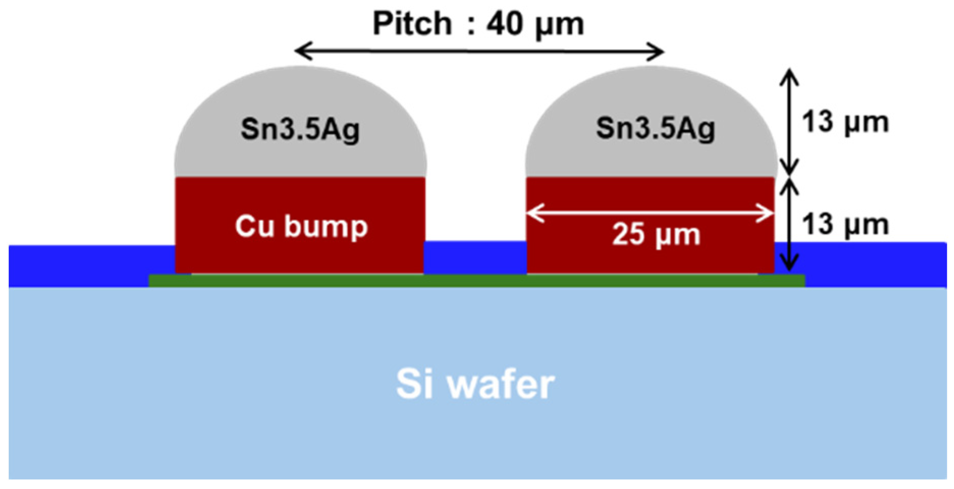
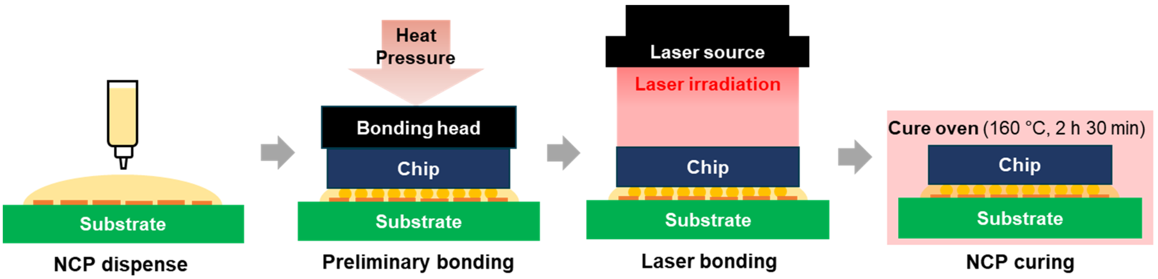
2. Materials and Methods
3. Results
3.1. Joint Properties with LAB Power Density
3.2. Mechanical Properties with LAB Power Density
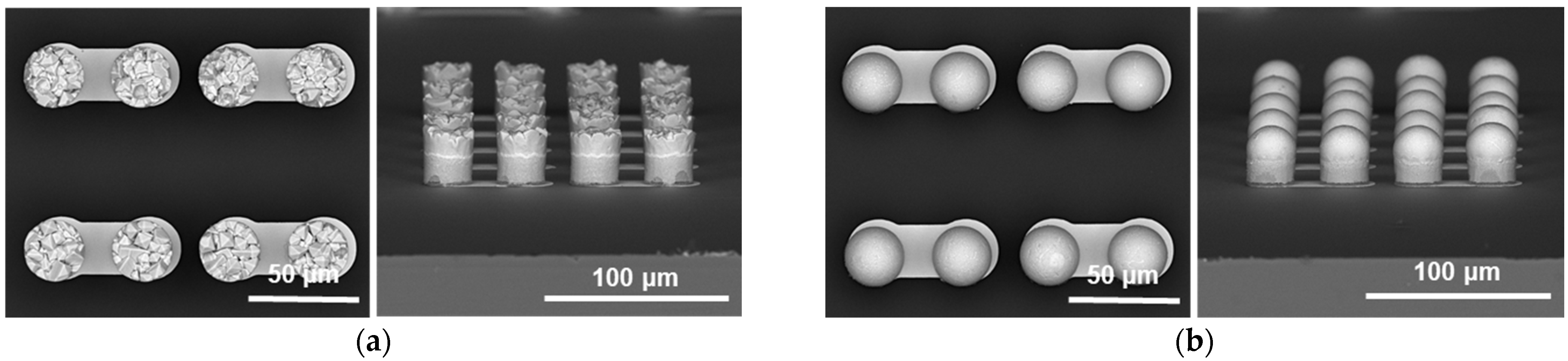
- Fracture mode 1: A fracture that occurs inside the SnAg solder;
- Fracture mode 2: A mixed fracture mode in the solder and Cu6Sn5 IMC;
- Fracture mode 3: A mixed fracture mode in the Cu6Sn5 IMC and Cu pad;
- Fracture mode 4: A fracture mode when solder splashing occurs.
- Fracture mode 1: A fracture that occurs inside the SnAg solder;
- Fracture mode 2: A mixed fracture mode in the solder and Ni3Sn4 IMC;
- Fracture mode 3: A mixed fracture mode in the Ni3Sn4 IMC and Ni;
- Fracture mode 4: A fracture mode when solder splash occurs.
4. Conclusions
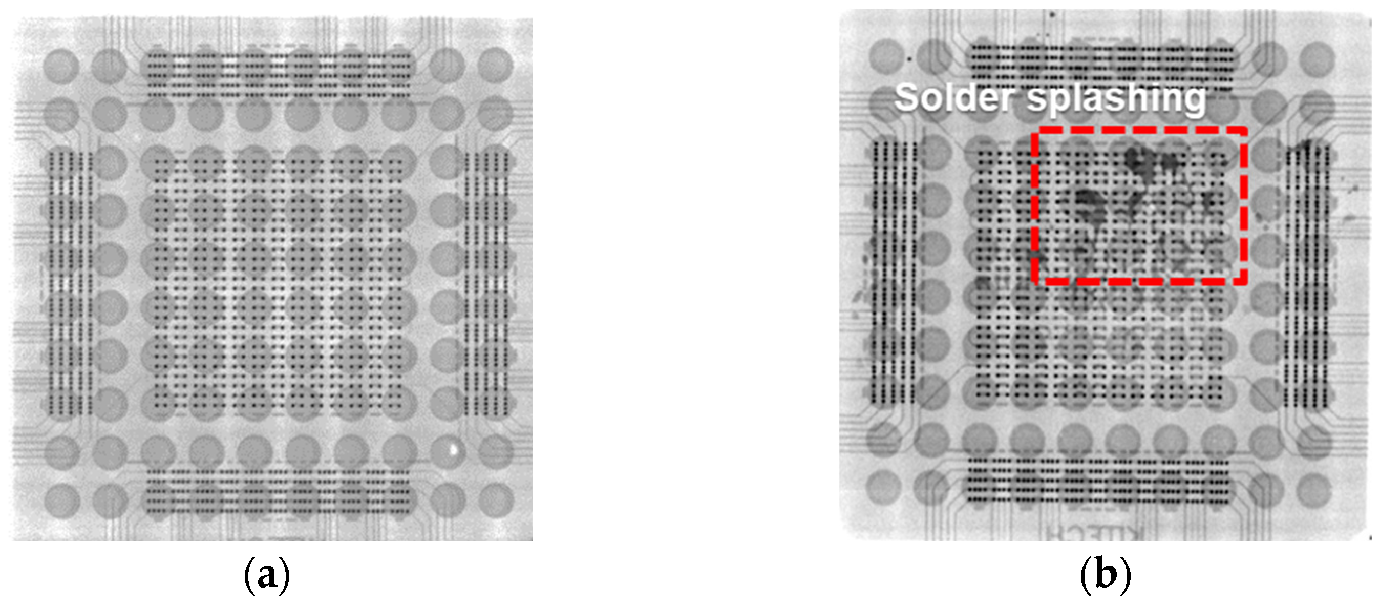
- High laser power density and irradiation time caused “solder splashing” where solder explosively vaporized and spread. This was particularly evident at 2.8 W/mm2 and 1.9 s, highlighting the need for precise laser parameter control.
- The DPIG showed IMC thickness and higher shear strength (22.69 MPa) compared to the ENEPIG, which had a shear strength of 25.67 MPa. The Ni layer in the ENEPIG acted as a diffusion barrier, resulting in thinner IMC growth.
- Mechanical performance: The LAB joints exhibited superior mechanical performance, with higher shear strength than the TCB and MR joints. The failure mechanisms shifted from solder to IMC-related fractures with increasing laser power density and irradiation time.
- Fine-pitch applications: LAB minimized the thermal stress and warpage, making it highly suitable for fine-pitch applications and high-performance semiconductor packaging.
Author Contributions
Funding
Institutional Review Board Statement
Informed Consent Statement
Data Availability Statement
Conflicts of Interest
References
- Lundstrom, M.S.; Alam, M.A. Moore’s law: The journey ahead. Science 2022, 378, 722–723. [Google Scholar] [CrossRef] [PubMed]
- Lau, J.H. Recent advances and trends in advanced packaging. IEEE Trans. Compon. Packag. Manuf. Technol. 2022, 12, 228–252. [Google Scholar] [CrossRef]
- Agarwal, R.; Cheng, P.; Shah, P.; Wilkerson, B.; Swaminathan, R.; Wuu, J.; Mandalapu, C. 3D packaging for heterogeneous integration. In Proceedings of the 2022 IEEE 72nd Electronic Components and Technology Conference (ECTC), San Diego, CA, USA, 31 May–3 June 2022; pp. 1103–1107. [Google Scholar] [CrossRef]
- Bajwa, A.A.; Jangam, S.; Pal, S.; Marathe, N.; Bai, T.; Fukushima, T.; Goorsky, M.; Iyer, S.S. Heterogeneous integration at fine pitch (≤ 10 um) using thermal compression bonding. In Proceedings of the 2017 IEEE 67th Electronic Components and Technology Conference (ECTC), Orlando, FL, USA, 30 May–2 June 2017; pp. 1276–1284. [Google Scholar] [CrossRef]
- Lee, S. Fundamentals of Thermal Compression Bonding Technology Andprocess Materials for 2.5/3D Packages BT-3D Microelectronic Packaging: From Fundamentals to Applications; Li, Y., Goyal, D., Eds.; Springer International Publishing: Cham, Switzerland, 2017; pp. 157–203. ISBN 978-3-319-44586-1. [Google Scholar]
- Jung, Y.; Ryu, D.; Gim, M.; Kim, C.; Song, Y.; Kim, J.; Yoon, J.; Lee, C. Development of next generation flip chip interconnection technology using homogenized laser-assisted bonding. In Proceedings of the 2016 IEEE 66th Electronic Components and Technology Conference (ECTC), Las Vegas, NV, USA, 31 May–3 June 2016; pp. 88–94. [Google Scholar] [CrossRef]
- Hsu, I.; Chen, C.Y.; Lin, S.; Yu, T.J.; Cho, N.J.; Hsieh, M.C. 7um chip-package interaction study on a fine pitch flip chip package with laser assisted bonding and mass reflow technology. In Proceedings of the 2019 IEEE 69th Electronic Components and Technology Conference (ECTC), Las Vegas, NV, USA, 28–31 May 2019; pp. 289–293. [Google Scholar] [CrossRef]
- Joo, H.S.; Min, K.D.; Lee, C.J.; Hwang, B.U.; Jung, S.B. Growth kinetics of intermetallic compound layers at the interface during laser-assisted bonding depending on surface finish. In Proceedings of the 2020 IEEE 70th Electronic Components and Technology Conference (ECTC), Orlando, FL, USA, 3–30 June 2020; pp. 1916–1921. [Google Scholar] [CrossRef]
- Choi, K.S.; Eom, Y.S.; Moon, S.H.; Joo, J.; Jeong, L.; Lee, K.; Kim, J.H.; Kim, J.H.; Yoon, G.S.; Lee, K.H.; et al. Enhanced performance of laser-assisted bonding with compression (LABC) compared with thermal compression bonding (TCB) technology. In Proceedings of the 2019 IEEE 69th Electronic Components and Technology Conference (ECTC), Las Vegas, NV, USA, 28–31 May 2019; pp. 197–203. [Google Scholar] [CrossRef]
- Alves Braganca, W.; Eom, Y.S.; Jang, K.S.; Moon, S.H.; Bae, H.C.; Choi, K.S. Collective laser-assisted bonding process for 3D TSV integration with NCP. ETRI J. 2019, 41, 396–407. [Google Scholar] [CrossRef]
- Gim, M.H.; Kim, C.H.; Na, S.H.; Ryu, D.S.; Park, K.R.; Kim, J.Y. High-performance flip chip bonding mechanism study with laser assisted bonding. In Proceedings of the 2020 IEEE 70th Electronic Components and Technology Conference (ECTC), Orlando, FL, USA, 3–30 June 2020; pp. 1025–1030. [Google Scholar] [CrossRef]
- Jang, Y.M.; Kim, Y.; Choa, S.H. Development and optimization of the laser-assistedbonding process for a flip chip package. Microsyst. Technol. 2020, 26, 1043–1054. [Google Scholar] [CrossRef]
- Shah, K. Reliable nickel-free surface finish solution for high-frequency, HDI PCB applications. J. Microelectron. Electron. Packag. 2020, 17, 121–127. [Google Scholar] [CrossRef]
- Cho, M.; Cho, J.; Kim, K.; Kim, S.Y.; Han, D.; Sung, T. Development trend of ni-less surface treatment technology for semiconductor packaging substrates. J. Microelectron. Packag. Soc. 2023, 30, 49–54. [Google Scholar]
- Gross, A.; Sitte, N. Nickel-free final finishes in the electronics industry. In Proceedings of the 2015 European Microelectronics Packaging Conference (EMPC), Friedrichshafen, Germany, 14–16 September 2015; pp. 2–5. [Google Scholar]
- Lee, T.Y.; Kim, J.; Jun, S.Y.; Ahn, B.J.; Han, D.G.; Yoo, S. Interfacial microstructure and brittle fracture behavior of Sn-based solder on novel nickel-less DEG and EPIG surface finishes. J. Mater. Sci. Mater. Electron. 2023, 34, 129. [Google Scholar] [CrossRef]
- Jun, S.Y.; Bang, J.H.; Kim, M.S.; Han, D.G.; Lee, T.Y.; Yoo, S. Thermo-compression bonding of Cu/SnAg pillar bumps with electroless palladium immersion gold (EPIG) surface finish. Materials 2023, 16, 1739. [Google Scholar] [CrossRef] [PubMed]
- Fields, R.J.; Low III, S.R.; Lucey, G.K. Physical and mechanical properties of intermetallic compounds commonly found in solderjoints. Proceedings of TMS Symposium, Cincinnati, OH, USA, 20–24 October 1991. [Google Scholar]
- Han, S.; Han, S.; Lee, T.-Y.; Lee, H.-J.; Yoo, S. Cu/SnAg pillar bump joints on Ni-less surface finish in laser assisted bonding (LAB). In Proceedings of the 2024 International Conference on Electronics Packaging (ICEP), Toyama, Japan, 17–20 April 2024. [Google Scholar] [CrossRef]
- Han, S.; Han, S.E.; Lee, T.Y.; Han, D.G.; Park, Y.B.; Yoo, S. Brittle fracture behavior of Sn-Ag-Cu solder joints with Ni-less surface finish via laser-assisted bonding. Materials 2024, 17, 3619. [Google Scholar] [CrossRef] [PubMed]


Disclaimer/Publisher’s Note: The statements, opinions and data contained in all publications are solely those of the individual author(s) and contributor(s) and not of MDPI and/or the editor(s). MDPI and/or the editor(s) disclaim responsibility for any injury to people or property resulting from any ideas, methods, instructions or products referred to in the content. |
© 2025 by the authors. Licensee MDPI, Basel, Switzerland. This article is an open access article distributed under the terms and conditions of the Creative Commons Attribution (CC BY) license (https://creativecommons.org/licenses/by/4.0/).
Share and Cite
Han, S.-E.; Choi, D.-G.; Han, S.; Lee, T.-Y.; Han, D.-G.; Lee, H.-J.; Yoo, S. Microstructural and Mechanical Characterization of Cu/SnAg Pillar Bumps with Ni-Less Surface Finish Utilizing Laser-Assisted Bonding (LAB). Materials 2025, 18, 1834. https://doi.org/10.3390/ma18081834
Han S-E, Choi D-G, Han S, Lee T-Y, Han D-G, Lee H-J, Yoo S. Microstructural and Mechanical Characterization of Cu/SnAg Pillar Bumps with Ni-Less Surface Finish Utilizing Laser-Assisted Bonding (LAB). Materials. 2025; 18(8):1834. https://doi.org/10.3390/ma18081834
Chicago/Turabian StyleHan, Sang-Eun, Dong-Gyu Choi, Seonghui Han, Tae-Young Lee, Deok-Gon Han, Hoo-Jeong Lee, and Sehoon Yoo. 2025. "Microstructural and Mechanical Characterization of Cu/SnAg Pillar Bumps with Ni-Less Surface Finish Utilizing Laser-Assisted Bonding (LAB)" Materials 18, no. 8: 1834. https://doi.org/10.3390/ma18081834
APA StyleHan, S.-E., Choi, D.-G., Han, S., Lee, T.-Y., Han, D.-G., Lee, H.-J., & Yoo, S. (2025). Microstructural and Mechanical Characterization of Cu/SnAg Pillar Bumps with Ni-Less Surface Finish Utilizing Laser-Assisted Bonding (LAB). Materials, 18(8), 1834. https://doi.org/10.3390/ma18081834