Article

Numerical Investigation of Perovskite/Silicon Heterojunction Tandem Solar Cell with a Dual-Functional Layer of MoOX

College of Materials Science and Engineering, Nanjing Tech University, Nanjing 211816, China
*
Author to whom correspondence should be addressed.
Materials 2025, 18(7), 1438; https://doi.org/10.3390/ma18071438
Submission received: 25 February 2025 / Revised: 19 March 2025 / Accepted: 20 March 2025 / Published: 24 March 2025
(This article belongs to the Special Issue Recent Advances in Semiconductors for Solar Cell Devices)

Abstract

:
This study proposed a novel perovskite/silicon heterojunction (SHJ) tandem device structure without an interlayer, represented as ITO/NiO/perovskite/SnO2/MoOX/i-a-Si:H/n-c-Si/i-a-Si:H/n-a-Si:H/Ag, which was investigated by Silvaco TCAD software. The recombination layer in this structure comprises the carrier transport layers of SnO2 and MoOX, where MoOX serves dual functions, acting as the emitter for the SHJ bottom cell and as part of the recombination layer in the tandem cell. First, the effects of different recombination layers are analyzed, and the SnO2/MoOX layer demonstrates the best performance. Then, we systematically investigated the impact of the carrier concentration, interface defect density, thicknesses of the SnO2/MoOX layer, different hole transport layers (HTLs) for the top cell, absorption layer thicknesses, and perovskite defect density on device performance. The optimal carrier concentration in the recombination layer should exceed 5 × 1019 cm−3, the interface defect density should be below 1 × 1016 cm−2, and the thicknesses of SnO2/MoOX should be kept at 20 nm/20 nm. CuSCN has been found to be the optimal HTL for the top cell. When the silicon absorption layer is 200 μm, the perovskite layer thickness is 470 nm, and the defect density of the perovskite layer is 1011 cm−3, the planar structure can achieve the best performance of 32.56%. Finally, we studied the effect of surface texturing on the SHJ bottom cell, achieving a power conversion efficiency of 35.31% for the tandem cell. Our simulation results suggest that the simplified perovskite/SHJ tandem solar cell with a dual-functional MoOX layer has the potential to provide a viable pathway for developing high-efficiency tandem devices.

1. Introduction

Crystalline silicon cells have dominated the solar market with a maximum efficiency of 27.3% [1], which is near their theoretical limit [2]. To surpass this limit, tandem cells have emerged as a key solution. This approach utilizes two or more single-junction cells stacked together to efficiently absorb the solar spectrum. Currently, the efficiency of single-junction perovskite cells has rapidly advanced, from 3.8% [3] in 2009 to 26.7% [4]. They exhibit superior performance, tunable energy bands, simple preparation, and low cost [5]. Naturally, the combination of perovskite and crystalline silicon cells in tandem devices has been an important research area. In fact, perovskite is widely used as the top cell in tandem solar cells, paired with bottom cells such as silicon [6], CIGS [7], organic device [8], and other perovskite cells [9] to form various tandem configurations. Among these tandem devices, perovskite/silicon cells have shown rapid progress in efficiency due to significant advances in material selection and structural optimization of top perovskite cells [10,11,12]. Their efficiency has been raised from an initial 13.7% [13] to 34.6% [14]. Except for the top cell, the design of the recombination layer is also critical for tandem devices, as it must facilitate both optical transmission and electrical connection [15].
Currently, there are three design strategies for the recombination layer for perovskite/silicon tandem devices. The most commonly used material in the recombination layer of tandem cells is transparent conductive oxide (TCO), such as indium tin oxide [16] (ITO), Indium Zinc Oxide [17] (IZO), and aluminum-doped zinc oxide [18] (AZO). Nevertheless, TCOs are susceptible to optical loss when it comes to ensuring high conductivity [19]. The second strategy is to employ silicon-based tunneling junctions, which are heavily doped in nano-crystalline silicon (nc-Si:H) [20,21]. These junctions offer high conductivity, excellent carrier selectivity, and reduced optical losses compared to TCOs. However, the preparation process of tunnel junctions is relatively complex and may affect the low-temperature process of SHJ bottom cells [22]. The third strategy is the interlayer-free design, which enables carrier extraction and recombination by completely removing the conventional recombination layer, allowing direct connection between the top and bottom cell’s the electron transport layer (ETL) or hole transport layer (HTL). This method simplifies the cell structure, reduces preparation costs, and avoids the optical loss of the conventional recombination layer.
The perovskite/silicon tandem solar cells without an interlayer have been reported [23,24,25,26], where the bottom cell is typically a homojunction, such as a Passivated Emitter and Rear Cell (PERC). SnO2 serves as both the ETL for the perovskite top cell and part of the recombination layer, forming an ohmic contact with the P⁺-Si emitter of the PERC bottom cell [27]. In this configuration, SnO2 functions as an electron transport, while the P⁺-Si layer is responsible for hole transport, enabling electron–hole recombination at the interface. Similarly, TiO2 has been employed as an ETL and recombination junction in perovskite/silicon tandem solar cells, where its impurity states assist recombination at the interface [28]. In these interlayer-free tandem devices, the silicon bottom cell is always a homojunction, where minority carriers tend to recombine at the interface, reducing the open-circuit voltage (VOC) [29]. In contrast, a silicon heterojunction (SHJ) cell can prevent minority carriers from recombining at the interface, thereby preserving the VOC of the silicon cell [30]. Therefore, SHJ cells can be used as better bottom ones which generally offer superior performance in tandem devices. In conventional perovskite/SHJ tandem cells, the interlayer is often a tunneling junction. However, nc-Si:H used in tunneling junctions leads to parasitic absorption due to its small bandgap [31]. Additionally, the amorphous silicon thin-film emitter of the SHJ cell absorbs some sunlight, also contributing to optical loss. Transition metal oxides (TMOs) can replace a-Si:H to address this issue [32]. For n-type SHJ bottom cells, MoOX, which has a high work function [33] and wide bandgap [34], can replace the doped p-type amorphous silicon layer as an emitter, reducing parasitic absorption and improving overall cell performance [35,36]. MoOX is also widely used as an HTL in single-junction perovskite cells. Moreover, it plays a role in the recombination layer in tandem cells such as all perovskite and perovskite/organic [8,37]. In these tandem cells, MoOX, together with Ag and/or ITO, forms the recombination layer. In perovskite/SHJ tandem cells, the interlayer-free design allows the electron transport layer (SnO2) of the top cell to be deposited directly on the MoOX layer, forming the recombination layer and eliminating the optical losses associated with tunnel junctions. In this configuration, holes collected by MoOX and electrons collected by SnO2 can be recombined at their interface. Thus, MoOX plays dual roles as both the emitter for the bottom cell and the recombination layer in the tandem cell. This innovative design has not been reported in perovskite/SHJ tandem devices. Here, our research goal is to develop high-performance tandem devices of perovskite/SHJ.
In this work, Silvaco TCAD [38,39,40] software was employed to simulate perovskite/SHJ tandem devices. First, four recombination layers in the perovskite/SHJ tandem structure are studied. Next, the influence of key parameters on cell performance is analyzed, including the carrier concentration and thickness of the SnO2/MoOX recombination layer, the defect density at the SnO2/MoOX interface, the HTL of the top cell, the thickness of the absorption layers, and the defect density of the perovskite layer. Finally, the impact of surface texturing on device performance is investigated.

2. Methods

2.1. Simulation Methodology

The simulation is performed using the Silvaco TCAD tool (version 2019), which is based on three fundamental equations, including the Poisson equation, the drift-diffusion equation, and the carrier continuity equation. By solving these equations, the spatial distributions of parameters such as hole and electron concentrations, electric potential, and others are obtained. These results are used to calculate the current density–voltage (J-V) curves. Then, the relevant electrical parameters of the device can be determined, including open-circuit voltage (VOC), short-circuit current density (JSC), fill factor (FF), and power conversion efficiency (PCE). The J-V curves are simulated under AM 1.5 G solar spectrum at 1000 W/m2 light intensity.

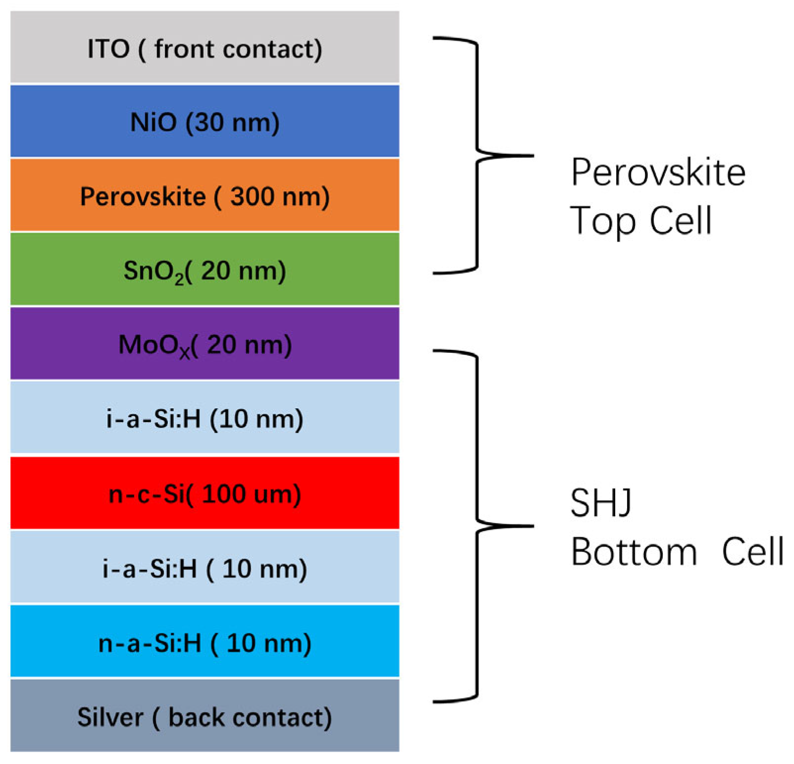
2.2. Device Structure

This tandem solar cell consists of an SHJ bottom cell and a perovskite top cell. As shown in Figure 1, the tandem device structure is as follows: ITO/NiO/perovskite/SnO2/MoOX/i-a-Si:H/n-c-Si/i-a-Si:H/n-a-Si:H/Ag. The material of FA0.83Cs0.17PbBr0.85I2.15, with a bandgap of 1.7 eV [41], is selected as the absorber layer in the top cell. The initial HTL of the top cell is NiO, and the ETL is SnO2. MoOX serves dual functions, not only acting as the emitter for the bottom cell but also participating in current recombination with SnO2.
Table 1 presents the electrical parameters used in the simulation of the perovskite/SHJ tandem device, sourced from the literature [41,42,43,44] and the Silvaco database. The optical constants (nk values) for NiO, perovskite, SnO2, and MoOX were obtained from References [45,46,47,48,49], while those for c-Si, a-Si:H, ITO, and Ag were chosen from the Silvaco database. Table 2 lists the defect parameter settings for the cell. Table 3 outlines the electrical parameters of different HTLs [50], and their optical constants are cited from References [51,52,53].

3. Results and Discussion

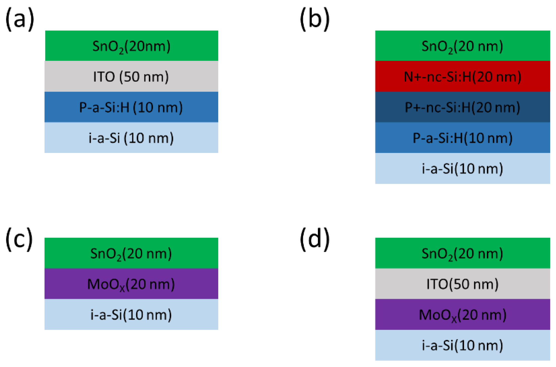
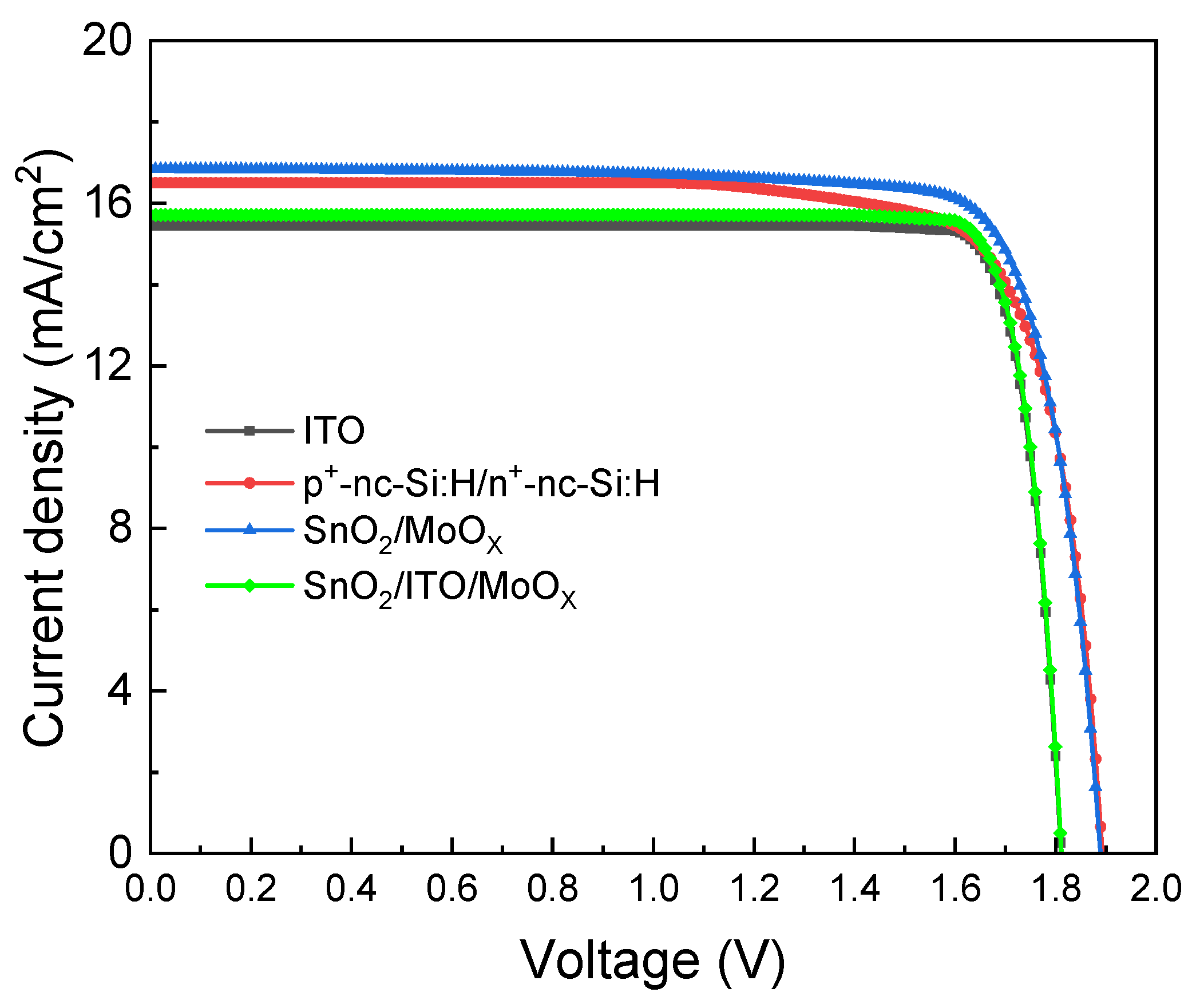
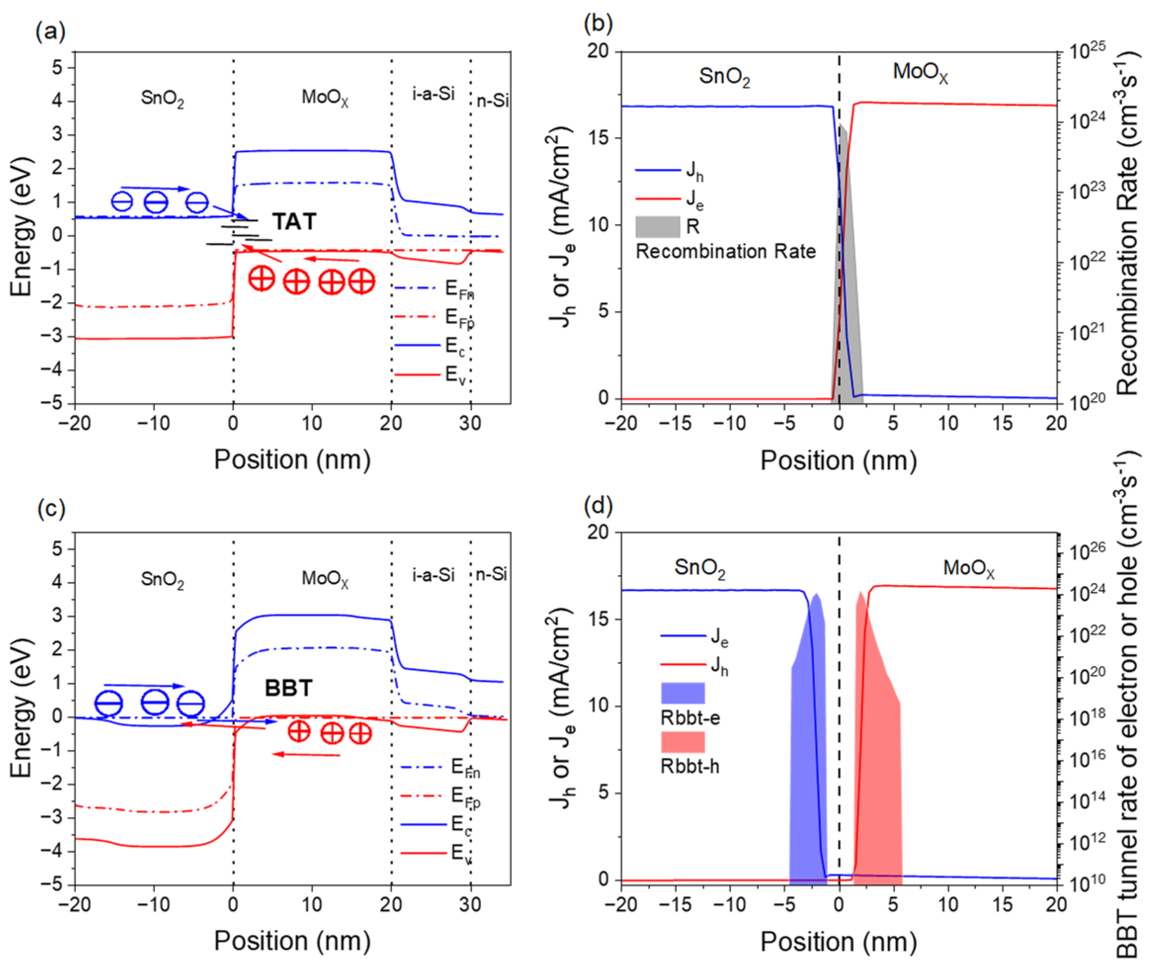
3.1. Effect of Different Recombination Layers

Four different structures of the recombination layer were compared, as illustrated in Figure 2. In Figure 2a, the intermediate recombination layer, ITO, is used to connect the top and bottom cells. Figure 2b shows a tunnel junction connecting the top and bottom cell, which includes n+-nc-Si:H and p+-nc-Si:H. Figure 2c represents the interlayer-free structure, where the ETL (SnO2) of the top cell and the HTL (MoOX) of the bottom cell are directly connected. Figure 2d shows a structure in which the intermediate layer, ITO, is inserted between MoOX and SnO2. The parameters for ITO and nc-Si:H are sourced from the Silvaco database.
As shown in Figure 3, the J-V curves demonstrate that the interlayer-free device has the best efficiency. Compared to the ITO and tunnel junction structures, this interlayer-free device reduces parasitic absorption, allowing for more effective light absorption. Regarding VOC, as shown in Table 4, the devices with an ITO intermediate layer exhibit a decrease in VOC due to the resistive shunting effect of the ITO layer. Additionally, the devices with the SnO2/MoOX recombination layer show a slight reduction in VOC compared to nc-Si:H tunnel junctions. This may be related to insufficient optimization of the recombination layer [23], which leads to the accumulation of un-recombined charges at the SnO2/MoOX interface, thereby affecting the overall performance of the device.

3.2. Effect of SnO2/MoOX Recombination Layer on Device Performance

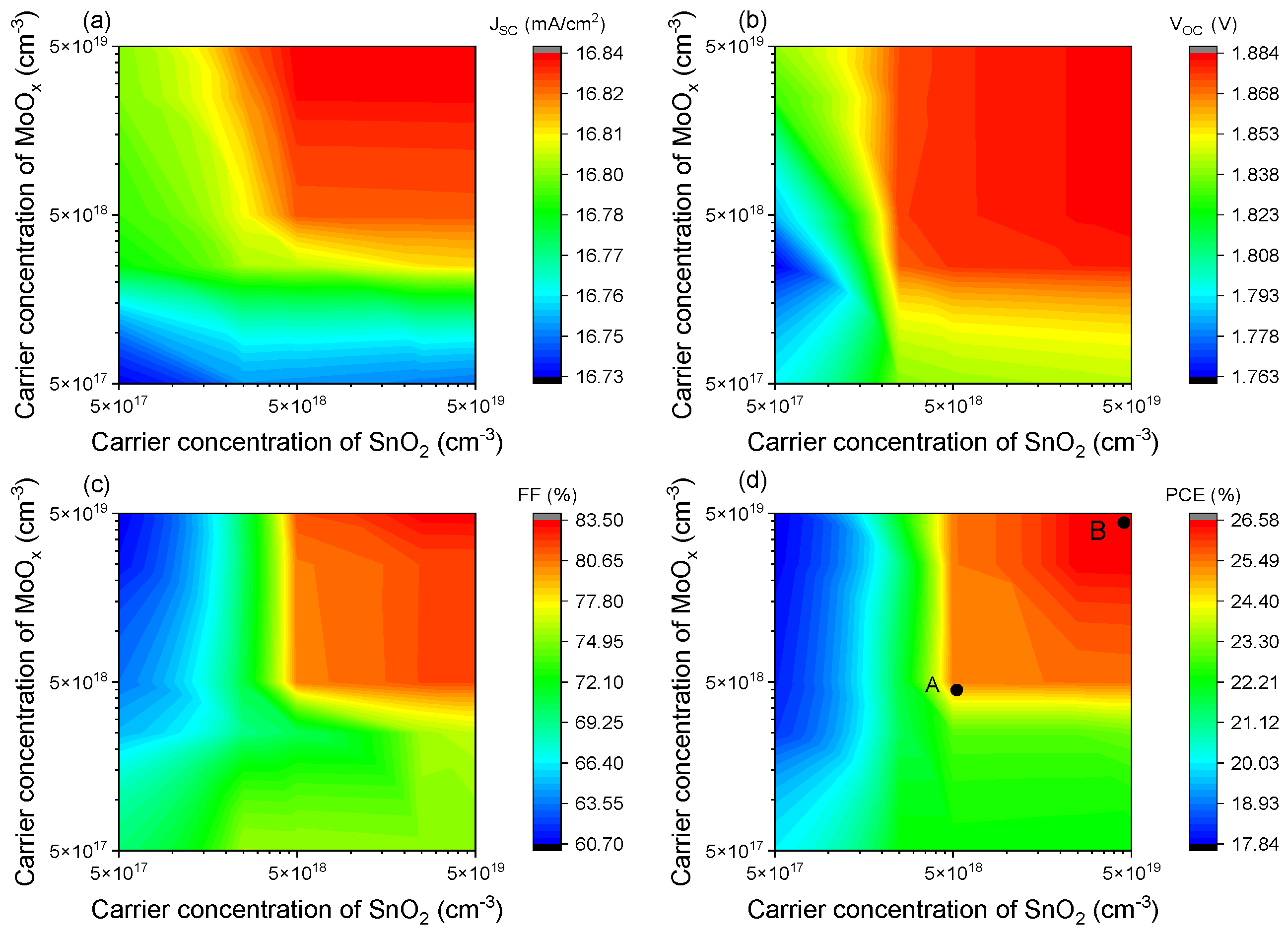
3.2.1. Effect of the Carrier Concentration of the Recombination Layer

The impact of SnO2 and MoOX carrier concentrations on tandem device performance has been studied. As shown in Figure 4, an increase in the carrier concentration of SnO2 and MoOX from 5 × 1017 cm−3 to 5 × 1019 cm−3 results in a monotonic rise in the four parameters: VOC, JSC, FF, and PCE. Cell performance is poor when the carrier concentration in the recombination layer is less than 5 × 1018 cm−3. The best efficiency of 26.58% is obtained when the carrier concentration of both the SnO2 and MoOX layers reaches 5 × 1019 cm−3.
To analyze the mechanism underlying the efficiency improvement with increasing carrier concentration in the recombination layer, points A and B in Figure 4d are selected, corresponding to the carrier concentrations of 5 × 1018 cm−3 and 5 × 1019 cm−3, respectively. Figure 5 shows the energy band diagrams and electron (hole) current density distributions for points A and B. The band alignment in the recombination layer determines whether charge transport occurs via band-to-band tunneling (BBT) or a trap-assisted tunneling (TAT) mechanism [54]. In the recombination layer, the carriers in the SnO2 layer are primarily electrons, while the carriers in the MoOX layer are holes. The energy band diagram in Figure 5a shows a clear separation between the quasi-Fermi level of electrons in SnO2 and that of holes in MoOX. There is no overlap between the valence band (EV) of MoOX and the conduction band (EC) of SnO2. From Figure 5b, we observe the electron–hole current density distribution and a high recombination rate at the SnO2/MoOX interface. These results suggest that the charge transport in the recombination layer occurs via TAT due to interface defects.
In contrast, Figure 5c shows an energy overlap between the EC of SnO2 and the EV of MoOX. The quasi-Fermi level of electrons in SnO2 aligns closely with that of holes in MoOX. In Figure 5d, a current-free region is observed at the SnO2/MoOX interface, indicating that charge transport in the recombination layer is dominated by the BBT mechanism. As the carrier concentration in the recombination layer increases from 5 × 1018 cm−3 to 5 × 1019 cm−3, the recombination mechanism changes from TAT to BBT. When the charge recombination mechanism is BBT, the tandem solar cell device achieves higher efficiency.

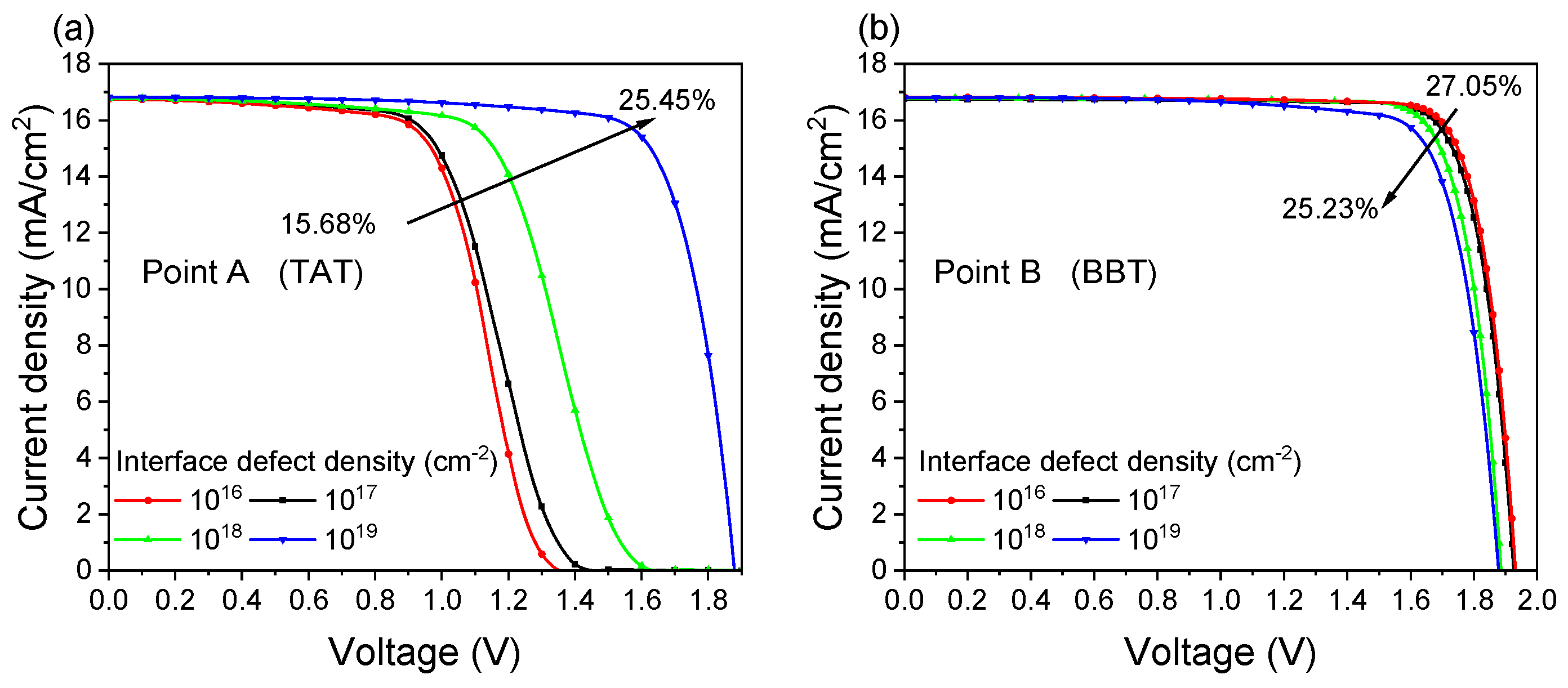
3.2.2. Effect of the Defect Density at the SnO2/MoOX Interface

This section investigates the impact of the defect density at the SnO2/MoOX interface on tandem device performance. Points A and B from the previous section are chosen for the analysis. For point A, as illustrated in Figure 6a, when the defect density at the recombination layer interface increases from 1 × 1016 cm−2 to 1 × 1019 cm−2, the cell efficiency is raised from 15.68% to 25.45%. Since the recombination mechanism at point A is dominated by TAT, a high interface defect density significantly enhances electron–hole recombination in the recombination layer, thereby improving the tandem device efficiency. However, for point B, dominated by BBT, increasing the interface defects results in a reduction in tandem cell efficiency. As illustrated in Figure 6b, the efficiency decreases from 27.05% to 25.23% when the defect density is changed from 1 × 1016 cm−2 to 1 × 1019 cm−2. Therefore, the optimal doping concentrations for SnO2 and MoOX are 5 × 1019 cm−3, and the ideal defect density at the SnO2/MoOX interface is 1 × 1016 cm−2.

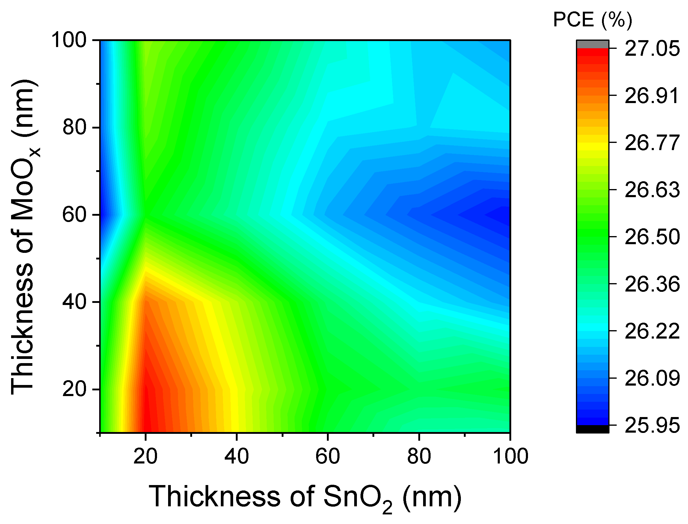
3.2.3. Effect of the Thickness of the Recombination Layer

This section examines the impact of SnO2/MoOX recombination layer thickness on tandem cell performance. Figure 7 illustrates the variation in device efficiency as the thicknesses of the SnO2 and MoOX layers are adjusted from 10 nm to 100 nm. When the thicknesses of the SnO2/MoOX layer are more than 20 nm/20 nm, the PCE declines. Notably, the MoOX layer is dual-functional, and the variations in its thickness can affect both its role as the emitter in the bottom cell and its involvement in electron–hole recombination. The recombination layer exhibits intrinsic optical absorption. Generally, an excessively thick recombination layer reduces cell efficiency due to optical absorption, while an overly thin film not only affects uniform converge but also impairs charge recombination. As shown in Figure 7, the optimal thicknesses for both the SnO2 and MoOX layers are approximately 20 nm, consistent with their initial thicknesses. Therefore, the thicknesses of the SnO2 and MoOX layers are set to 20 nm each, and the optimized device can achieve a PCE of 27.05%, in agreement with previous results in Section 3.2.2.

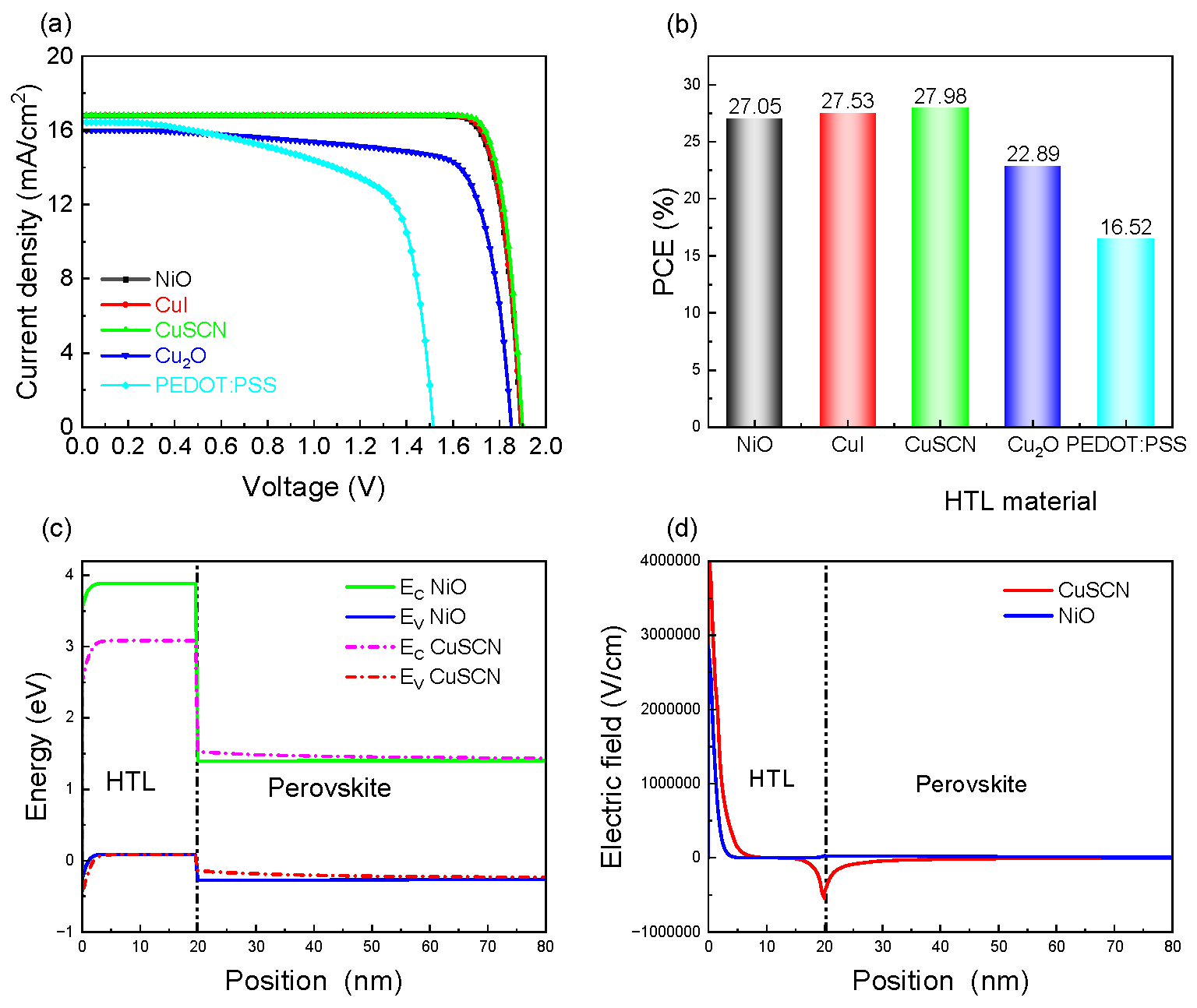
3.3. Effect of Different HTLs on the Top Cell

This section investigates the effect of different HTLs on the top cell on the device performance. The HTLs include NiO, CuI, Cu2O, CuSCN, and Poly(3,4-ethylenedioxythiophene)/Poly(styrenesulfonate) (PEDOT:PSS). The relevant parameters for each HTL are shown in Table 3. Figure 8a presents the J-V curves for these HTLs, while Figure 8b shows the corresponding tandem solar cell efficiency, and CuSCN exhibits the best efficiency of 27.98%. To analyze the reasons for the improved cell performance when CuSCN replaces NiO, Figure 8c compares the energy band diagrams of CuSCN and NiO as HTLs. The valence band offset (VBO) represents the difference between the valence band of the HTL and that of the perovskite layer, which is calculated as VBO = EV(HTL) − EV(perovskite). A negative VBO corresponds to a cliff-like band alignment. As shown in Figure 8c, the NiO/perovskite interface has a cliff of −0.55 eV. The cliff-like band structure does not prevent carrier extraction from the perovskite layer. However, a large cliff significantly increases the recombination rate at the interface [55]. In contrast, CuSCN is used as the HTL, which results in a smaller VBO (−0.45 eV) with the perovskite layer. Thus interface recombination can be reduced, and the efficiency can then be improved from 27.05% to 27.98%. Figure 8d shows the electric field at the HTL/perovskite interface when using CuSCN and NiO as HTLs. With CuSCN as the HTL, the electric field at the interface is broader and stronger, facilitating hole transport. Therefore, CuSCN is chosen as the optimal HTL for the perovskite top cell.

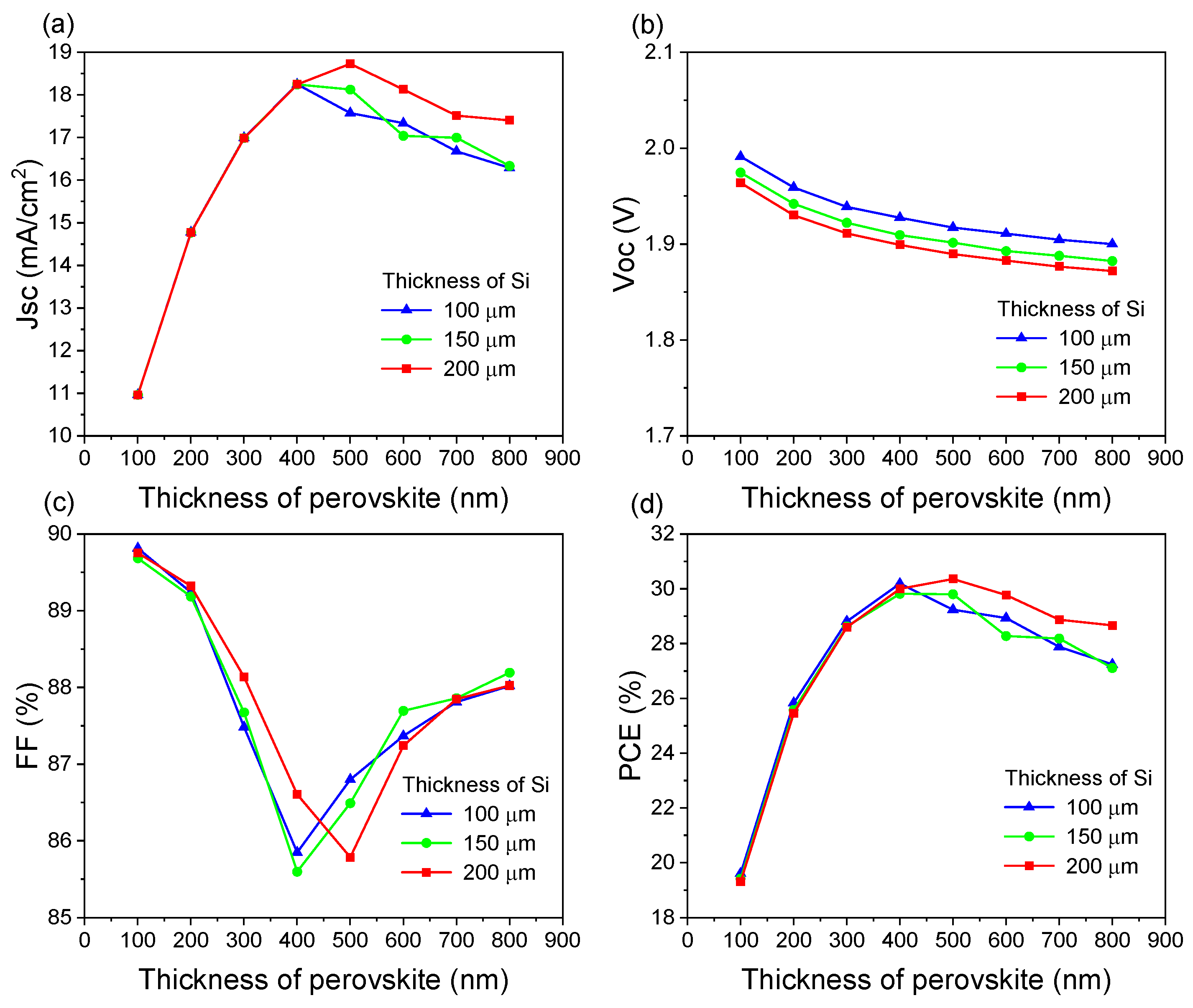
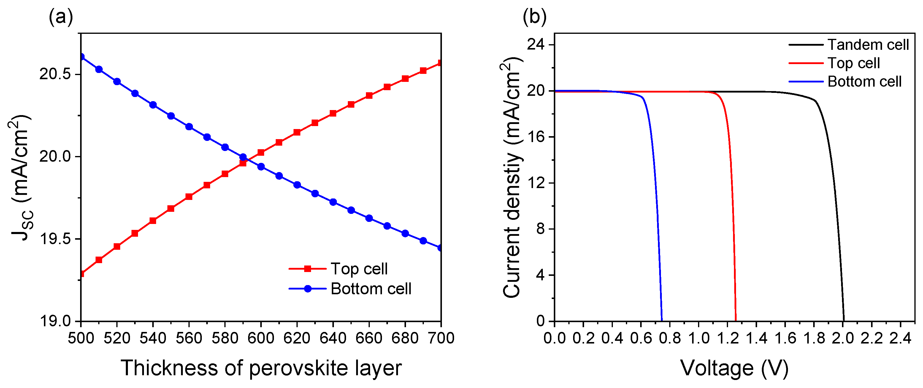
3.4. Effect of the Thicknesses of Perovskite and Silicon Absorption Layers

In a tandem device, modifying the absorption layer thickness in the sub-cells causes deviations from the current-matching condition. This deviation significantly affects the photovoltaic characteristics of the tandem device. As shown in Figure 9a, when the perovskite layer thickness increases from 100 nm to 400 nm, the JSC shows an upward trend. However, when the thickness increases from 500 nm to 800 nm, the JSC gradually decreases. When the perovskite layer thickness is below 400 nm, the current is limited by the top cell, and increasing the thickness of the absorption layer in the SHJ bottom cell does not effectively increase the overall current output. On the other hand, when the perovskite layer thickness exceeds 400 nm, the bottom cell becomes the limiting factor for device performance. Therefore, as the SHJ bottom cell absorption layer thickness becomes thicker, the optimal thickness of the top cell absorption layer for maximum JSC also increases. For instance, when the thickness of the bottom cell absorption layer is 100 μm, the optimal perovskite thickness becomes 400 nm, and for the 200 μm silicon absorption layer, it is 500 nm. Correspondingly, the current density increases from 18.1 to 18.7 mA/cm2.
Regarding VOC, as shown in Figure 9b, increasing the absorption layer thickness slightly decreases VOC. As the absorption layer thickness increases, carrier recombination can be enhanced, resulting in VOC reduction. As shown in Figure 9c, FF varies differently from JSC. As the perovskite layer thickness increases, FF first decreases, reaching a minimum value at the current-matching point, and then it increases again, suggesting that FF variation is closely related to the degree of current matching between sub-cells [56]. As shown in Figure 9d, the trend in PCE is similar to that of JSC. As the perovskite layer thickness increases, PCE first increases and then decreases, primarily due to the increase in JSC. When the absorption layer is 500 nm in the top cell and the absorption layer is 200 μm in bottom cell, the tandem device achieves the highest PCE of 30.56% under the condition of current matching.

3.5. Effect of the Defect Density of the Perovskite Absorber Layer

The defect density of the top cell absorber layer has an impact on tandem device performance. Figure 10a demonstrates the J-V curves under varying defect densities of the perovskite absorber layer. Figure 10b shows a significant degradation in tandem cell efficiency from 32.56% to 11.04% as the defect density increases from 1011 cm−3 to 1017 cm−3. As shown in Figure 10c, the current-matching point remains achievable through perovskite thickness optimization when the defect density is not more than 1014 cm⁻³, as evidenced by the intersection points in their current density curves. However, once the defect density exceeds 1014 cm−3, the current-matching point is no longer achievable, and the efficiency of the tandem device deteriorates rapidly. Under this non-ideal condition, the JSC of the tandem device is limited by the top cell, and we define the top cell absorber layer thickness at the maximum JSC as the ‘pseudo-matching thickness’ when the JSC difference between sub-cells is the smallest. Figure 10d shows that when the defect density is enlarged from 1011 cm−3 to 1014 cm−3, the optimal thickness of the perovskite layer increases from 470 nm to 490 nm under the condition of current matching, and the pseudo-matching thickness decreases after the defect density of 1014 cm−3. Therefore, when the thickness and the defect density of the perovskite layer are 470 nm and 1011 cm−3, respectively, the best performance of the tandem cell can reach 32.56%.

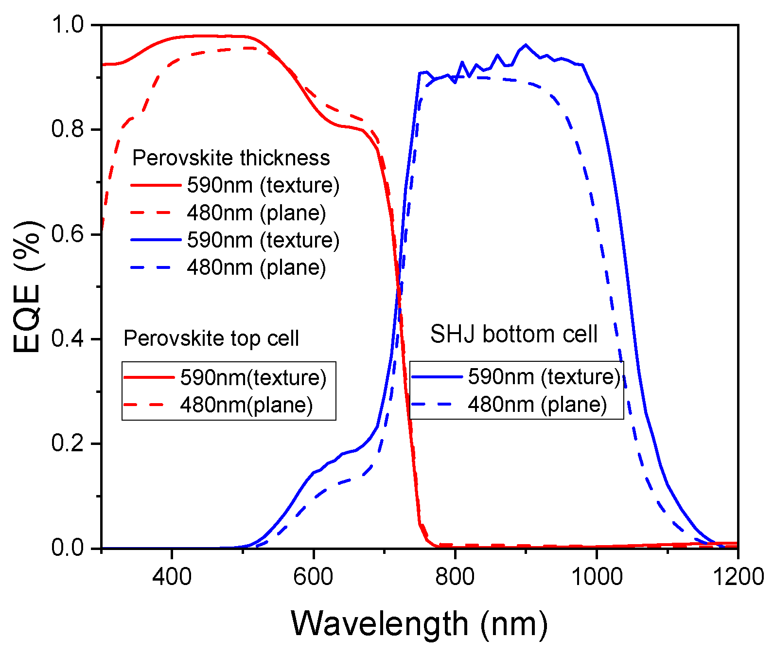
3.6. Effect of Bottom Cell Texture Structure

Finally, we consider the actual tandem solar cell device structure, in which the perovskite top cell is deposited on the textured SHJ bottom cell. Consequently, the previous planar model is converted into a textured one. The front surface of the SHJ bottom cell features a pyramidal texture, characterized by a pyramid angle of 54.74°, width of 3.536 μm, and height of 5 μm. The crystalline silicon layer in the bottom cell retains a thickness of 200 μm. As shown in Figure 11a, the current-matching point is achieved at a 590 nm perovskite absorber thickness, corresponding to a JSC of 20.23 mA/cm2. Figure 11b illustrates the J-V curves of the tandem cell and its sub-cells at the matching point, where the JSC of the sub-cells and the tandem cell are nearly identical. As summarized in Table 5, the tandem cell exhibits a VOC of 2.01 V and a PCE of 35.31%, closely matching the sum of the performance of the two sub-cells. To explore the reason for efficiency improvement by texture structure, Figure 12 compares the external quantum efficiency (EQE) of the textured and planar structures at the current-matching point. The textured structure enhances the absorption in the bottom cell above 900 nm and the top cell below 400 nm, leading to performance improvement.

4. Conclusions

This study established a model for perovskite/SHJ tandem solar cells using Silvaco TCAD software. The initial cell structure is ITO/NiO/perovskite/SnO2/MoOX/i-a-Si:H/n-c-Si/i-a-Si:H/n-a-Si:H/Ag, where MoOX plays dual roles, serving as the emitter for the SHJ bottom cell and participating in charge recombination. First, we investigated the impact of different recombination layers on tandem cell performance, identifying the SnO2/MoOX recombination layer as the optimal choice. When the doping concentrations of SnO2/MoOX layers are increased from 5 × 1018 cm−3 to 5 × 1019 cm−3, the recombination mechanism shifts from the less efficient TAT to the more efficient BBT, leading to significant improvement in tandem solar cell performance. Under the BBT mechanism, the optimal performance is achieved with a defect density of 1 × 1016 cm−2 at the SnO2/MoOX interface and the thicknesses of 20 nm/20 nm, reaching 27.05%. Next, by using CuSCN as the HTL to enhance device performance in the top cell, the efficiency is further improved to 27.82%. Thickness optimization of the top and bottom absorption layers can increase the efficiency to 30.56%. Additionally, by reducing the defect density of the perovskite layer to 1011 cm−3, the efficiency is raised to 32.56%. Finally, by applying a pyramidal texture to the front surface of the SHJ bottom cell, the tandem cell efficiency reaches 35.31%. These results demonstrate the potential of perovskite/SHJ tandem solar cells with a dual-functional layer of MoOX.

Author Contributions

Formal analysis, T.-Y.L. and J.W.; investigation, T.-Y.L.; methodology, T.-Y.L., J.W. and X.-D.F.; supervision, X.-D.F.; validation, J.W.; writing—original draft, T.-Y.L.; writing—review and editing, X.-D.F. All authors have read and agreed to the published version of the manuscript.

Funding

This work was supported by the priority academic program development of the Jiangsu Higher Education Institution (PAPD).

Institutional Review Board Statement

Not applicable.

Informed Consent Statement

Not applicable.

Data Availability Statement

The original contributions presented in this study are included in the article. Further inquiries can be directed to the corresponding author.

Conflicts of Interest

The authors declare no conflicts of interest.

References

  1. Wu, H.; Ye, F.; Yang, M.; Luo, F.; Tang, X.; Tang, Q.; Qiu, H.; Huang, Z.; Wang, G.; Sun, Z.; et al. Silicon heterojunction back-contact solar cells by laser patterning. Nature 2024, 635, 604–609. [Google Scholar] [CrossRef]
  2. Richter, A.; Hermle, M.; Glunz, S.W. Reassessment of the Limiting Efficiency for Crystalline Silicon Solar Cells. IEEE J. Photovolt. 2013, 3, 1184–1191. [Google Scholar] [CrossRef]
  3. Kojima, A.; Teshima, K.; Shirai, Y.; Miyasaka, T. Organometal Halide Perovskites as Visible-Light Sensitizers for Photovoltaic Cells. J. Am. Chem. Soc. 2009, 131, 6050–6051. [Google Scholar] [CrossRef] [PubMed]
  4. Green, M.A.; Dunlop, E.D.; Yoshita, M.; Kopidakis, N.; Bothe, K.; Siefer, G.; Hao, X.; Jiang, J.Y. Solar Cell Efficiency Tables (Version 65). Prog. Photovoltaics Res. Appl. 2025, 33, 3–15. [Google Scholar] [CrossRef]
  5. Liang, C.; Gu, H.; Xia, Y.; Wang, Z.; Liu, X.; Xia, J.; Zuo, S.; Hu, Y.; Gao, X.; Hui, W.; et al. Two-dimensional Ruddlesden–Popper layered perovskite solar cells based on phase-pure thin films. Nat. Energy 2021, 6, 38–45. [Google Scholar] [CrossRef]
  6. Heydarian, M.; Messmer, C.; Bett, A.J.; Heydarian, M.; Chojniak, D.; Kabaklı, Ö.Ş.; Tutsch, L.; Bivour, M.; Siefer, G.; Schubert, M.C.; et al. Maximizing Current Density in Monolithic Perovskite Silicon Tandem Solar Cells. Sol. RRL 2023, 7, 2200930. [Google Scholar] [CrossRef]
  7. Jacobsson, T.J.; Hultqvist, A.; Svanström, S.; Riekehr, L.; Cappel, U.B.; Unger, E.; Rensmo, H.; Johansson, E.M.J.; Edoff, M.; Boschloo, G. 2-Terminal CIGS-perovskite tandem cells: A layer by layer exploration. Sol. Energy 2020, 207, 270–288. [Google Scholar] [CrossRef]
  8. Maksudov, T.; He, M.; Doukas, S.; Nugraha, M.I.; Adilbekova, B.; Faber, H.; Luo, L.; Zhou, R.; Bakr, O.M.; Ogieglo, W.; et al. 23.6% Efficient perovskite-organic tandem photovoltaics enabled by recombination layer engineering. Mater. Sci. Eng. R. Rep. 2024, 159, 100802. [Google Scholar] [CrossRef]
  9. Hossain, M.I.; Saleque, A.M.; Ahmed, S.; Saidjafarzoda, I.; Shahiduzzaman, M.; Qarony, W.; Knipp, D.; Biyikli, N.; Tsang, Y.H. Perovskite/perovskite planar tandem solar cells: A comprehensive guideline for reaching energy conversion efficiency beyond 30%. Nano Energy 2021, 79, 105400. [Google Scholar] [CrossRef]
  10. Al-Ashouri, A.; Köhnen, E.; Li, B.; Magomedov, A.; Hempel, H.; Caprioglio, P.; Márquez, J.A.; Vilches, A.B.M.; Kasparavicius, E.; Smith, J.A.; et al. Monolithic perovskite/silicon tandem solar cell with >29% efficiency by enhanced hole extraction. Science 2020, 370, 1300–1309. [Google Scholar] [CrossRef]
  11. Tockhorn, P.; Sutter, J.; Cruz, A.; Wagner, P.; Jaeger, K.; Yoo, D.; Lang, F.; Grischek, M.; Li, B.; Li, J.; et al. Nano-optical designs for high-efficiency monolithic perovskite-silicon tandem solar cells. Nat. Nanotechnol. 2022, 17, 1214–1221. [Google Scholar] [CrossRef] [PubMed]
  12. Hou, Y.; Aydin, E.; De Bastiani, M.; Xiao, C.; Isikgor, F.H.; Xue, D.-J.; Chen, B.; Chen, H.; Bahrami, B.; Chowdhury, A.H.; et al. Efficient tandem solar cells with solution-processed perovskite on textured crystalline silicon. Science 2020, 367, 1135. [Google Scholar] [CrossRef] [PubMed]
  13. Mailoa, J.P.; Bailie, C.D.; Johlin, E.C.; Hoke, E.T.; Akey, A.J.; Nguyen, W.H.; McGehee, M.D.; Buonassisi, T. A 2-terminal perovskite/silicon multijunction solar cell enabled by a silicon tunnel junction. Appl. Phys. Lett. 2015, 106, 121105. [Google Scholar] [CrossRef]
  14. Best Research-Cell Efficiency Chart. Available online: https://www.nrel.gov/pv/cell-efficiency.html (accessed on 2 January 2025).
  15. De Bastiani, M.; Subbiah, A.S.; Aydin, E.; Isikgor, F.H.; Allen, T.G.; De Wolf, S. Recombination junctions for efficient monolithic perovskite-based tandem solar cells: Physical principles, properties, processing and prospects. Mater. Horiz. 2020, 7, 2791–2809. [Google Scholar] [CrossRef]
  16. Ying, Z.; Yang, Z.; Zheng, J.; Wei, H.; Chen, L.; Xiao, C.; Sun, J.; Shou, C.; Qin, G.; Sheng, J.; et al. Monolithic perovskite/black-silicon tandems based on tunnel oxide passivated contacts. Joule 2022, 6, 2644–2661. [Google Scholar] [CrossRef]
  17. Ying, Z.Q.; Yang, X.; Zheng, J.M.; Zhu, Y.D.; Xiu, J.W.; Chen, W.; Shou, C.H.; Sheng, J.; Zeng, Y.H.; Yan, B.J.; et al. Charge-transfer induced multifunctional BCP:Ag complexes for semi-transparent perovskite solar cells with a record fill factor of 80.1%. J. Mater. Chem. A 2021, 9, 12009–12018. [Google Scholar] [CrossRef]
  18. Palmstrom, A.F.; Eperon, G.E.; Leijtens, T.; Prasanna, R.; Habisreutinger, S.N.; Nemeth, W.; Gaulding, E.A.; Dunfield, S.P.; Reese, M.; Nanayakkara, S.; et al. Enabling Flexible All-Perovskite Tandem Solar Cells. JOULE 2019, 3, 2193–2204. [Google Scholar] [CrossRef]
  19. Kabakli, O.S.; Kox, J.; Tutsch, L.; Heydarian, M.; Bett, A.J.; Lange, S.; Fischer, O.; Hagendorf, C.; Bivour, M.; Hermle, M.; et al. Minimizing electro-optical losses of ITO layers for monolithic perovskite silicon tandem solar cells. Sol. Energy Mater. Sol. Cells 2023, 254, 112246. [Google Scholar] [CrossRef]
  20. Sahli, F.; Kamino, B.A.; Werner, J.; Bräuninger, M.; Paviet-Salomon, B.; Barraud, L.; Monnard, R.; Seif, J.P.; Tomasi, A.; Jeangros, Q.; et al. Improved Optics in Monolithic Perovskite/Silicon Tandem Solar Cells with a Nanocrystalline Silicon Recombination Junction. Adv. Energy Mater. 2018, 8, 1701609. [Google Scholar] [CrossRef]
  21. Sahli, F.; Werner, J.; Kamino, B.A.; Bräuninger, M.; Monnard, R.; Paviet-Salomon, B.; Barraud, L.; Ding, L.; Diaz Leon, J.J.; Sacchetto, D.; et al. Fully textured monolithic perovskite/silicon tandem solar cells with 25.2% power conversion efficiency. Nat. Mater. 2018, 17, 820–826. [Google Scholar] [CrossRef]
  22. Aydin, E.; Allen, T.G.; De Bastiani, M.; Xu, L.; Ávila, J.; Salvador, M.; Van Kerschaver, E.; De Wolf, S. Interplay between temperature and bandgap energies on the outdoor performance of perovskite/silicon tandem solar cells. Nat. Energy 2020, 5, 851–859. [Google Scholar] [CrossRef]
  23. Zheng, J.; Lau, C.F.J.; Mehrvarz, H.; Ma, F.-J.; Jiang, Y.; Deng, X.; Soeriyadi, A.; Kim, J.; Zhang, M.; Hu, L.; et al. Large area efficient interface layer free monolithic perovskite/homo-junction-silicon tandem solar cell with over 20% efficiency. Energy Environ. Sci. 2018, 11, 2432–2443. [Google Scholar] [CrossRef]
  24. Hyun, J.; Yeom, K.M.; Lee, H.E.; Kim, D.; Lee, H.-S.; Noh, J.H.; Kang, Y. Efficient n-i-p Monolithic Perovskite/Silicon Tandem Solar Cells with Tin Oxide via a Chemical Bath Deposition Method. Energies 2021, 14, 7614. [Google Scholar] [CrossRef]
  25. Li, W.; Zheng, J.; Hu, B.; Fu, H.-C.; Hu, M.; Veyssal, A.; Zhao, Y.; He, J.-H.; Liu, T.L.; Ho-Baillie, A.; et al. High-performance solar flow battery powered by a perovskite/silicon tandem solar cell. Nat. Mater. 2020, 19, 1326–1331. [Google Scholar] [CrossRef]
  26. Zheng, J.; Mehrvarz, H.; Ma, F.-J.; Lau, C.F.J.; Green, M.A.; Huang, S.; Ho-Baillie, A.W.Y. 21.8% Efficient Monolithic Perovskite/Homo-Junction-Silicon Tandem Solar Cell on 16 cm2. ACS Energy Lett. 2018, 3, 2299–2300. [Google Scholar] [CrossRef]
  27. Hoye, R.L.Z.; Bush, K.A.; Oviedo, F.; Sofia, S.E.; Thway, M.; Li, X.; Liu, Z.; Jean, J.; Mailoa, J.P.; Osherov, A.; et al. Developing a Robust Recombination Contact to Realize Monolithic Perovskite Tandems With Industrially Common p-Type Silicon Solar Cells. IEEE J. Photovolt. 2018, 8, 1023–1028. [Google Scholar] [CrossRef]
  28. Shen, H.; Omelchenko, S.T.; Jacobs, D.A.; Yalamanchili, S.; Wan, Y.; Yan, D.; Phang, P.; The, D.; Wu, Y.; Yin, Y.; et al. In situ recombination junction between p-Si and TiO2 enables high-efficiency monolithic perovskite/Si tandem cells. Sci. Adv. 2018, 4, eaau9711. [Google Scholar] [CrossRef]
  29. Yan, D.; Cuevas, A.; Wan, Y.; Bullock, J. Passivating contacts for silicon solar cells based on boron-diffused recrystallized amorphous silicon and thin dielectric interlayers. Sol. Energy Mater. Sol. Cells 2016, 152, 73–79. [Google Scholar] [CrossRef]
  30. Melskens, J.; Loo, B.W.H.v.d.; Macco, B.; Black, L.E.; Smit, S.; Kessels, W.M.M. Passivating Contacts for Crystalline Silicon Solar Cells: From Concepts and Materials to Prospects. IEEE J. Photovolt. 2018, 8, 373–388. [Google Scholar] [CrossRef]
  31. Köhler, M.; Pomaska, M.; Procel, P.; Santbergen, R.; Zamchiy, A.; Macco, B.; Lambertz, A.; Duan, W.; Cao, P.; Klingebiel, B.; et al. A silicon carbide-based highly transparent passivating contact for crystalline silicon solar cells approaching efficiencies of 24%. Nat. Energy 2021, 6, 529–537. [Google Scholar] [CrossRef]
  32. He, J.; Wang, G.; Qiu, Y.; Tang, Z.; Ye, F.; Zhang, C.; Wang, S.; Cai, L.; Yu, T.; Gao, P. Enabling Transparent-Conductive-Oxide Free Efficient Heterojunction Solar Cells by Flexibly Using Dopant-Free Contact. Adv. Funct. Mater. 2022, 32, 2205901. [Google Scholar] [CrossRef]
  33. Meyer, J.; Hamwi, S.; Kröger, M.; Kowalsky, W.; Riedl, T.; Kahn, A. Transition Metal Oxides for Organic Electronics: Energetics, Device Physics and Applications. Adv. Mater. 2012, 24, 5408–5427. [Google Scholar] [CrossRef] [PubMed]
  34. Chuang, S.; Battaglia, C.; Azcatl, A.; McDonnell, S.; Kang, J.S.; Yin, X.; Tosun, M.; Kapadia, R.; Fang, H.; Wallace, R.M.; et al. MoS2 P-type Transistors and Diodes Enabled by High Work Function MoOx Contacts. Nano Lett. 2014, 14, 1337–1342. [Google Scholar] [CrossRef] [PubMed]
  35. Hao, L.-C.; Zhang, M.; Ni, M.; Liu, J.-M.; Feng, X.-D. Simulation of high efficiency silicon heterojunction solar cells with molybdenum oxide carrier selective layer. Mater. Res. Express 2018, 5, 075504. [Google Scholar] [CrossRef]
  36. Dréon, J.; Jeangros, Q.; Cattin, J.; Haschke, J.; Antognini, L.; Ballif, C.; Boccard, M. 23.5%-efficient silicon heterojunction silicon solar cell using molybdenum oxide as hole-selective contact. Nano Energy 2020, 70, 104495. [Google Scholar] [CrossRef]
  37. Brinkmann, K.O.; Becker, T.; Zimmermann, F.; Kreusel, C.; Gahlmann, T.; Theisen, M.; Haeger, T.; Olthof, S.; Tückmantel, C.; Günster, M.; et al. Perovskite–organic tandem solar cells with indium oxide interconnect. Nature 2022, 604, 280–286. [Google Scholar] [CrossRef]
  38. Li, P.; Xiong, H.; Lin, L.; Jiang, L.; Kang, Z.; Yan, Q.; Lien, S.-Y.; Chen, H.; Qiu, Y. Modeling and simulation of bifacial perovskite/PERT-silicon tandem solar cells. Solar Energy 2021, 227, 292–302. [Google Scholar] [CrossRef]
  39. Salgado-Conrado, L.; Álvarez-Macías, C.; Reyes-Durán, B. A Review of Simulation Tools for Thin-Film Solar Cells. Materials 2024, 17, 5213. [Google Scholar] [CrossRef]
  40. Restat, L.; Messmer, C.; Heydarian, M.; Heydarian, M.; Schoen, J.; Schubert, M.C.; Glunz, S.W. Optoelectrical Modeling of Perovskite/Perovskite/Silicon Triple-Junction Solar Cells: Toward the Practical Efficiency Potential. Solar Rrl 2024, 8, 2300887. [Google Scholar] [CrossRef]
  41. Prathapani, S.; Bhargava, P.; Mallick, S. Electronic band structure and carrier concentration of formamidinium–cesium mixed cation lead mixed halide hybrid perovskites. Appl. Phys. Lett. 2018, 112, 092104. [Google Scholar] [CrossRef]
  42. Li, W.; Li, W.; Feng, Y.; Yang, C. Numerical analysis of the back interface for high efficiency wide band gap chalcopyrite solar cells. Sol. Energy 2019, 180, 207–215. [Google Scholar] [CrossRef]
  43. Bacha, M.; Saadoune, A.; Youcef, I.; terghini, O. Design and numerical investigation of Perovskite/Silicon tandem solar cell. Opt. Mater. 2022, 131, 112671. [Google Scholar] [CrossRef]
  44. Hossain, M.K.; Rubel, M.H.K.; Toki, G.F.I.; Alam, I.; Rahman, M.F.; Bencherif, H. Effect of Various Electron and Hole Transport Layers on the Performance of CsPbI3-Based Perovskite Solar Cells: A Numerical Investigation in DFT, SCAPS-1D, and wxAMPS Frameworks. ACS Omega 2022, 7, 43210–43230. [Google Scholar] [CrossRef]
  45. Kumar, A.; Dutta, M.; Tomer, S.; Rao, P.; Vandana; Srivastava, S.K.; Singh, S.N.; Pathi, P. Tuning of structural and optical properties of reactively sputtered MoOx films. J. Mater. Sci. Mater. Electron. 2024, 35, 612. [Google Scholar] [CrossRef]
  46. Koushik, D.; Jošt, M.; Dučinskas, A.; Burgess, C.; Zardetto, V.; Weijtens, C.; Verheijen, M.A.; Kessels, W.M.M.; Albrecht, S.; Creatore, M. Plasma-assisted atomic layer deposition of nickel oxide as hole transport layer for hybrid perovskite solar cells. J. Mater. Chem. C 2019, 7, 12532–12543. [Google Scholar] [CrossRef]
  47. Kuang, Y.; Zardetto, V.; van Gils, R.; Karwal, S.; Koushik, D.; Verheijen, M.A.; Black, L.E.; Weijtens, C.; Veenstra, S.; Andriessen, R.; et al. Low-Temperature Plasma-Assisted Atomic-Layer-Deposited SnO2 as an Electron Transport Layer in Planar Perovskite Solar Cells. ACS Appl. Mater. Interfaces 2018, 10, 30367–30378. [Google Scholar] [CrossRef]
  48. Werner, J.; Nogay, G.; Sahli, F.; Yang, T.C.-J.; Bräuninger, M.; Christmann, G.; Walter, A.; Kamino, B.A.; Fiala, P.; Löper, P.; et al. Complex Refractive Indices of Cesium–Formamidinium-Based Mixed-Halide Perovskites with Optical Band Gaps from 1.5 to 1.8 eV. ACS Energy Lett. 2018, 3, 742–747. [Google Scholar] [CrossRef]
  49. Jannat, F.; Ahmed, S.; Alim, M.A. Performance analysis of cesium formamidinium lead mixed halide based perovskite solar cell with MoOx as hole transport material via SCAPS-1D. Optik 2021, 228, 166202. [Google Scholar] [CrossRef]
  50. Alanazi, T.I.; Eid, O.I.; Okil, M. Numerical study of flexible perovskite/Si tandem solar cell using TCAD simulation. Opt. Quantum Electron. 2023, 55, 1152. [Google Scholar] [CrossRef]
  51. Fentahun, D.A.; Tyagi, A.; Kar, K.K. Numerically investigating the AZO/Cu2O heterojunction solar cell using ZnO/CdS buffer layer. Optik 2021, 228, 166228. [Google Scholar] [CrossRef]
  52. Tang, H.; Shang, Y.; Zhou, W.; Peng, Z.; Ning, Z. Energy Level Tuning of PEDOT:PSS for High Performance Tin-Lead Mixed Perovskite Solar Cells. Sol. RRL 2019, 3, 1800256. [Google Scholar] [CrossRef]
  53. Sun, B.; Chen, H.; Yan, K.; Feng, X.-D. Numerical investigation of the Cu2O solar cell with double electron transport layers and a hole transport layer. Opt. Mater. 2022, 131, 112642. [Google Scholar] [CrossRef]
  54. Procel, P.; Xu, H.; Saez, A.; Ruiz-Tobon, C.; Mazzarella, L.; Zhao, Y.; Han, C.; Yang, G.; Zeman, M.; Isabella, O. The role of heterointerfaces and subgap energy states on transport mechanisms in silicon heterojunction solar cells. Prog. Photovolt. Res. Appl. 2020, 28, 935–945. [Google Scholar] [CrossRef]
  55. Yang, Z.; Yang, W.; Yang, X.; Greer, J.C.; Sheng, J.; Yan, B.; Ye, J. Device physics of back-contact perovskite solar cells. Energy Environ. Sci. 2020, 13, 1753–1765. [Google Scholar] [CrossRef]
  56. Boccard, M.; Ballif, C. Influence of the Subcell Properties on the Fill Factor of Two-Terminal Perovskite–Silicon Tandem Solar Cells. ACS Energy Lett. 2020, 5, 1077–1082. [Google Scholar] [CrossRef]
Figure 1. Device structure of the perovskite/SHJ tandem cell.
Materials 18 01438 g001
Figure 2. Schematic structure of different recombination layer designs: (a) ITO, (b) p+-nc-Si:H/ n+-nc-Si:H, (c) SnO2/MoOX, and (d) SnO2/ITO/MoOX.
Materials 18 01438 g002
Figure 3. Comparison of J-V curves of tandem cells with different recombination layers.
Materials 18 01438 g003
Figure 4. Effect of carrier concentration in the SnO2/MoOX recombination layer on device performance of tandem cells: (a) JSC, (b) VOC, (c) FF, and (d) PCE.
Materials 18 01438 g004
Figure 5. (a) Energy band diagram of point A, (b) electron–hole current density distribution and recombination rate distribution at point A, (c) energy band diagram of point B, and (d) electron–hole current density distribution and tunneling rate distribution at point B.
Materials 18 01438 g005
Figure 6. J-V curves under different interface defect densities. (a) Point A: SnO2/MoOX doping concentration at 5 × 1018 cm−3. (b) Point B: SnO2/MoOX doping concentration at 5 × 1019 cm−3.
Materials 18 01438 g006
Figure 7. Effect of the thicknesses of SnO2/MoOX recombination layer on the PCE of the tandem device.
Materials 18 01438 g007
Figure 8. (a) J-V curves, (b) PCE, (c) energy band diagrams, and (d) electric field diagrams of tandem cells with NiO and CuSCN.
Materials 18 01438 g008
Figure 9. Effect of different top and bottom cell absorber layer thicknesses on tandem cell performance parameters: (a) JSC, (b) VOC, (c) FF, and (d) PCE.
Materials 18 01438 g009
Figure 10. Tandem cell performance under different defect densities (a) J-V curves, (b) PCE, (c) JSC of sub-cells with different perovskite thicknesses, and (d) optimal perovskite thickness.
Materials 18 01438 g010
Figure 11. (a) JSC of sub-cells as a function of perovskite thickness. (b) J-V curves of the tandem and its sub-cells under the condition of current matching.
Materials 18 01438 g011
Figure 12. EQE curves of the sub-cells under current-matching point.
Materials 18 01438 g012
Table 1. The material parameters of perovskite/SHJ tandem solar cells used in the simulation.
ParametersNiOPerovskiteSnO2n-c-Sii-a-Si:Hn-a-Si:HMoOX
Thickness (um)0.030.30.021000.010.010.02
Bandgap, Eg (eV)1.41.791.121.721.723
Electron affinity, χ (eV)3.84.054.44.053.863.862.5
Relative permittivity, ε10.76.53.611.811.811.85.6
Effective conduction band density,
NC (cm−3)
2.8 × 10191 × 10204 × 10182.8 × 10181 × 10201 × 10202.8 × 1018
Effective valance band density,
NV (cm−3)
1 × 10191 × 10201 × 10181 × 10191 × 10201 × 10202 × 1019
Mobility of electrons, μn (cm2/Vs)128.16101240202025
Mobility of holes, μp (cm2/Vs)2.881045155100
Donor doping density, ND (cm−3)--1 × 10185 × 1015-1 × 10¹⁸-
Acceptor doping density, NA (cm−3)1 × 10181 × 1016----1 × 10¹⁸
Lifetime of electron, τn (s)1 × 10−71 × 10−61 × 10−71 × 10−61 × 10−51 × 10−71 × 10−6
Lifetime of hole, τp (s)1 × 10−71 × 10−61 × 10−71 × 10−61 × 10−51 × 10−71 × 10−6
Table 2. Defect parameters of the layers and interfaces.
ParametersBulk DefectsInterface Defects
NiOPerovskiteSnO2NiO/PerovskitePerovskite/SnO2SnO2/MoOX
Defect typeAcceptorAcceptorDonorAcceptorAcceptorNeutral
Energy levelMidgapMidgapMidgapMidgapMidgapMidgap
Defect density1 × 1016 cm−31 × 1014 cm−31 × 1016 cm−31 × 1013 cm−21 × 1013 cm−21 × 1018 cm−2
Table 3. The material parameters of HTLs.
ParametersCuICuSCNCu2OPEDOT:PSS
Thickness (nm)20202020
Bandgap, Eg (eV)2.13.62.12.2
Electron affinity, χ (eV)2.981.73.22.9
Relative permittivity, ε6.5107.13
Mobility of electrons, μn (cm2/Vs)1001001110.02
Mobility of holes, μp (cm2/Vs)43.925800.02
Acceptor doping density, NA (cm−3)1 × 10181 × 10181 × 10181 × 1018
Effective conduction band density, NC (cm−3)2.8 × 10192.2 × 10192.5 × 10192.2 × 1015
Effective valance band density, NV (cm−3)1 × 10191.8 × 10181.8 × 10192.2 × 1019
Table 4. Tandem cell performance with different recombination layers.
Recombination LayerJSC (mA/cm2)VOC (V)FF (%)PCE (%)
ITO15.451.8188.0424.63
p+-nc-Si:H/n+-nc-Si:H16.511.8979.3124.78
SnO2/MoOX16.821.8780.525.45
SnO2/ITO/MoOX15.721.8187.925.04
Table 5. Performance parameters of top, bottom, and tandem cell.
JSC (mA/cm2)VOC (V)FF (%)PCE (%)
Perovskite top cell20.231.26688.8422.75
SHJ bottom cell20.300.74285.0512.81
Perovskite/SHJ tandem cell20.232.00886.9235.31
Disclaimer/Publisher’s Note: The statements, opinions and data contained in all publications are solely those of the individual author(s) and contributor(s) and not of MDPI and/or the editor(s). MDPI and/or the editor(s) disclaim responsibility for any injury to people or property resulting from any ideas, methods, instructions or products referred to in the content.

