
Research into the Failure Mechanism and Reliability of an Active Frequency-Selective Surface in Complex Environments


Abstract
1. Introduction
2. Materials and Methods
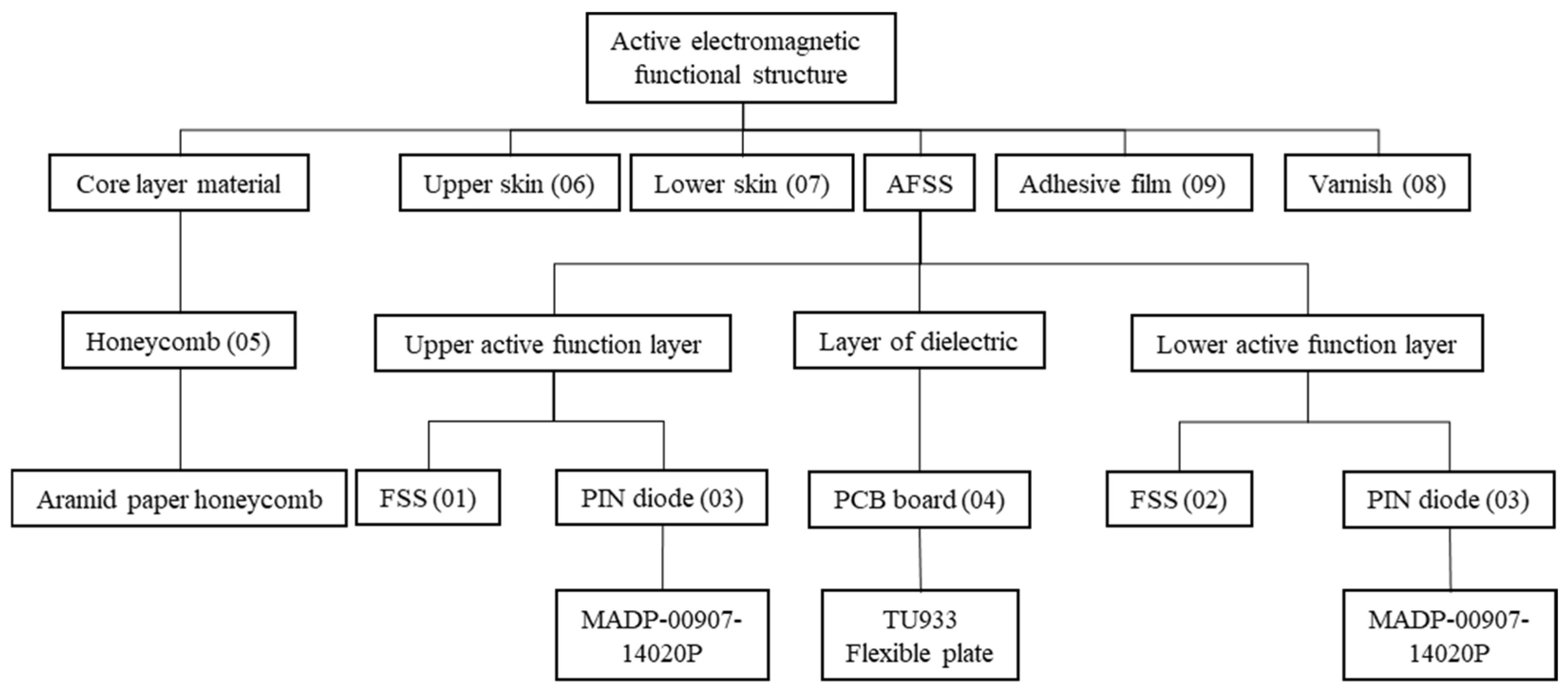
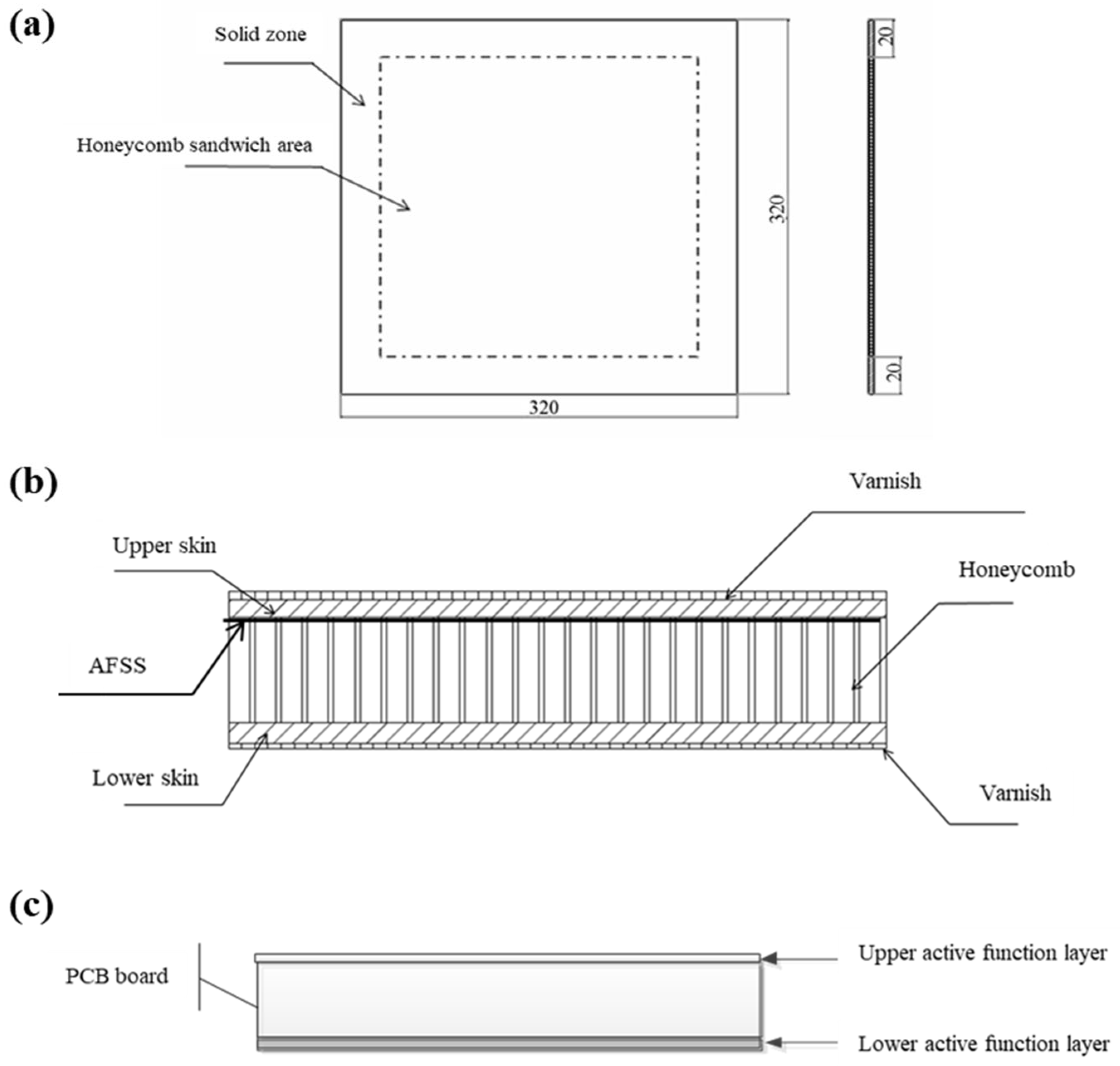
2.1. The Basic AFSS Structure
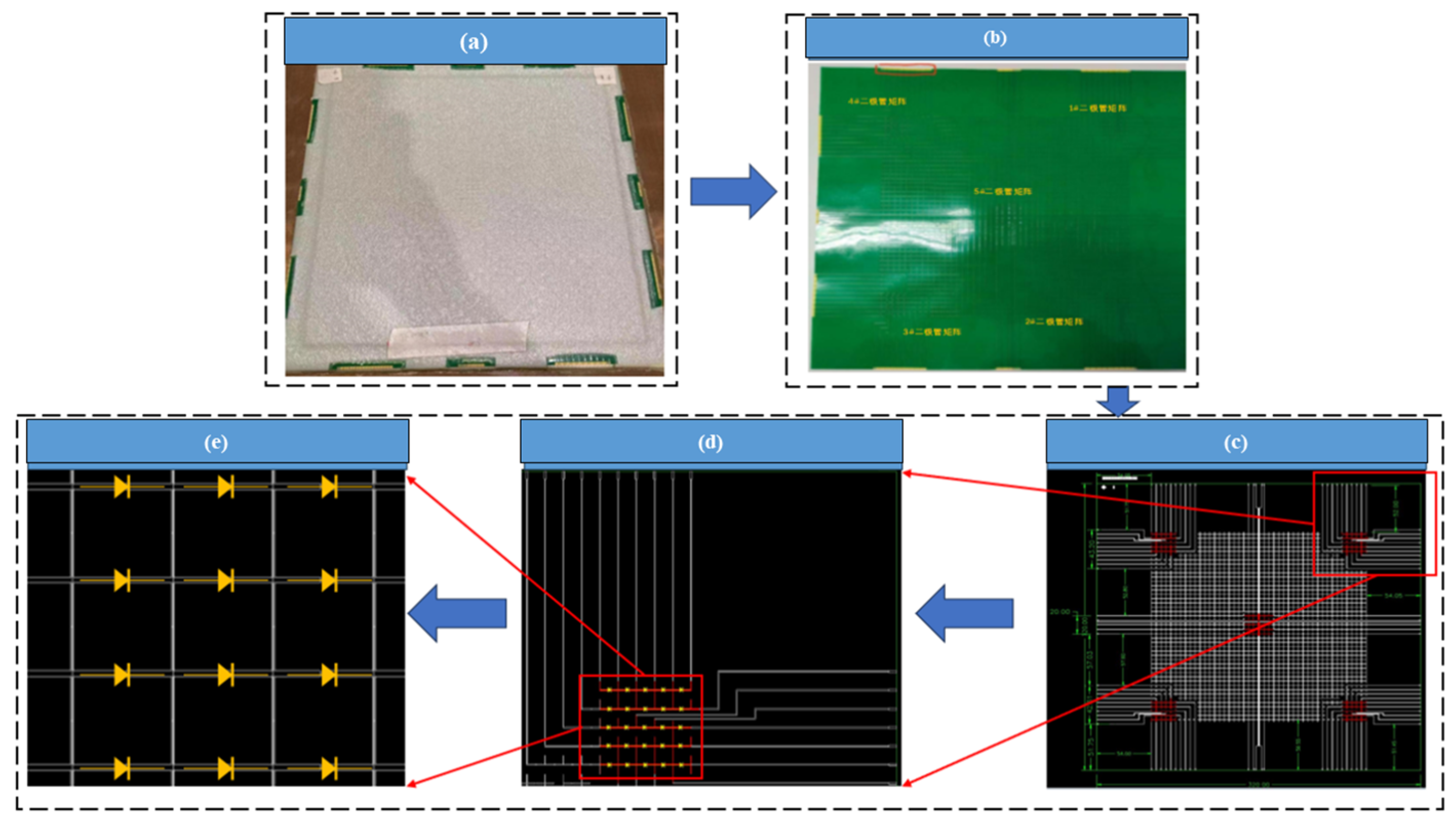
2.2. Test Sample and Test System Design
2.3. Design and Implementation of the AFSS Structure Fault Excitation Test
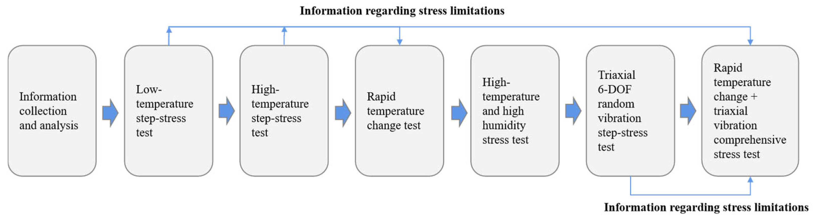
2.3.1. Design of the Test Scheme
2.3.2. Test Process
3. Results and Discussion
3.1. Test Results
3.2. Analysis of the AFSS Structure Failure Mode and Mechanism
4. Conclusions
Author Contributions
Funding
Institutional Review Board Statement
Informed Consent Statement
Data Availability Statement
Acknowledgments
Conflicts of Interest
Abbreviations
| AFSS | Active frequency-selective surface |
| MEMS | Microelectromechanical system |
| FSS | Frequency-selective surface |
| FMEA | Fault mode impact and hazard analysis |
| FA | Failure analysis |
| HALT | Highly accelerated life testing |
| RET | Reliability enhancement testing |
| PCBA | Printed circuit board assembly |
| PCB | Printed circuit board |
References
- Chang, T.K.; Langley, R.J.; Parker, E.A. An active square loop frequency selective surface. IEEE Microw. Guid. Wave Lett. 1993, 3, 387–388. [Google Scholar] [CrossRef]
- Ekmekci, E.; Topalli, K.; Akin, T.; Turhan-Sayan, G. A tunable multi-band metamaterial design using micro-split SRRstructures. Opt. Express 2009, 18, 16046–16058. [Google Scholar] [CrossRef] [PubMed]
- Zeng, X.; Zhang, L.; Wan, G. Analysis of the tunable wave-absorbing properties based on active frequency selective surface. China Shipbuild. Res. 2020, 15, 36–41. [Google Scholar]
- Taylor, P.S.; Parker, E.A.; Batchelor, J.C. An active annular ring frequency selective surface. IEEE Trans. Antennas Propagat. 2011, 59, 3265–3271. [Google Scholar] [CrossRef]
- Ghosh, S.; Srivastava, K.V. A polarisation-independent switchable absorber/reflector. Electron. Lett. 2016, 52, 1141–1143. [Google Scholar] [CrossRef]
- Ghosh, S.; Srivastava, K.V. Polarization-insensitive single- and broadband switchable absorber/reflector and its realization using a novel biasing technique. IEEE Trans. Antennas Propag. 2016, 64, 3665–3670. [Google Scholar] [CrossRef]
- Chen, Z.; Qiao, H.; Chen, Q.; Chen, X. A wideband and high-gain switched-beam antenna system using active frequency selective surface. IET Microw. Antennas Propag. 2023, 17, 1056–1061. [Google Scholar] [CrossRef]
- Shah, G.; Abidin, Z.U.; Cao, Q. A high angle stable and polarization symmetric dual band reconfigurable frequency selective surface. Frequenz 2023, 77, 29–38. [Google Scholar] [CrossRef]
- Zhang, Y.P.; Zhao, X.P.; Bao, S.; Luo, C.R. Dendritic metamaterial absorber based on impedance matching conditions. Acta Phys. Sin. 2010, 59, 6078–6083. [Google Scholar] [CrossRef]
- Han, X.; Gao, X. Design of multi-frequency composite structure metamaterial absorber. J. Guilin Univ. Electron. Sci. Technol. 2015, 35, 1–5. [Google Scholar]
- Zhang, P.C.; Lin, X.Q.; Shen, R. Research on Broadband Absorber Based on New Artificial Electromagnetic Materials. J. New Ind. 2013. [Google Scholar]
- Zhou, K. Design and Implementation of Flexible Wideband Tunable Microwave Absorber. Master’s Thesis, Huazhong University of Science and Technology, Wuhan, China, 2015. [Google Scholar]
- Pang, Y.; Wang, J.; Cheng, Q.; Xia, S.; Zhou, X.Y.; Xu, Z.; Cui, T.J.; Qu, S. Thermally tunable water-substrate broadband metamaterial absorbers. Appl. Phys. Lett. 2017, 110, 104103. [Google Scholar] [CrossRef]
- Yang, J.; Qu, S.; Ma, H.; Wang, J.; Pang, Y. Dual-band tunable infrared metamaterial absorber with VO2 conformal resonators. Opt. Commun. 2017, 402, 518–522. [Google Scholar] [CrossRef]
- Wu, X.; Hu, C.; Wang, Y.; Pu, M.; Huang, C.; Wang, C.; Luo, X. Active microwave absorber with the dual-ability of dividable modulation in absorbing intensity and frequency. AIP Adv. 2013, 3, 1626. [Google Scholar] [CrossRef]
- Junxie, F. Research on Light-Controlled Active Frequency Selective Surface. Master’s Thesis, Nanjing University of Aeronautics and Astronautics, Nanjing, China, 2018. [Google Scholar]
- Ren, W.; Wang, P.; Hu, R. Design of wave-absorbing frequency selective structure based on metamaterial technology. J. Beijing Inst. Technol. 2022, 42, 864–870. [Google Scholar]
- Jiang, Y.; Wang, Y.; Ge, D.; Li, S.; Cao, W.; Gao, X.; Yu, X. A graphene-based ultra-wideband absorber. Chin. Phys. Acta 2016, 65, 054101. [Google Scholar] [CrossRef]
- Hu, R.; Wang, J.; Wu, Q. A square symmetric metamaterial terahertz multi-frequency absorber. Prog. Lasers Optoelectron. 2022, 59, 0516001. [Google Scholar] [CrossRef]
- Zhou, Z.; Wang, J.; Pang, C.; Hao, G.; Feng, D. Study on the scattering characteristics of an electromagnetic control angular reflector. J. Radio Sci. 2023, 38, 921–928. [Google Scholar]
- Liu, C.; Li, G.X.; Xiao, W.S.; Liu, J.; Tan, L.P.; Li, C.J.; Wang, T.; Yang, F.R.; Xue, C. Reliability analysis of subsea control system using FMEA and FFTA. Sci. Rep. 2024, 14, 21353. [Google Scholar] [CrossRef]
- Wismer, S.E.; Jimenez, A.; Al-Douri, A.; Grabovetska, V.; Groth, K.M. PEM electrolyzer failure scenarios identified by failure modes and effects analysis (FMEA). Int. J. Hydrogen Energy 2024, 89, 1280–1289. [Google Scholar] [CrossRef]
- Zhang, X.; Han, J.; Zhao, J.; Wang, Y.; Guan, T. Development status and Application Prospect of High Accelerated Life Test Technology. Equip. Environ. Eng. 2020, 17, 13–19. [Google Scholar]
- Zhang, H.Y.; Lv, N.; Pei, Y.S. Research on the Application of Reliability Enhancement Testing Technology in Electronic Product Testing. China New Technol. Prod. 2020, 76–77. [Google Scholar]
- Zhang, L.; Luo, Y.W.; Qiu, Z.W. Overview of Reliability Technology Development Based on HALT and HASS Testing. Electron. Prod. Reliab. Environ. Test. 2022, 40, 87–91. [Google Scholar]
- Yan, Y.J.; Wang, X.H.; Zhao, G.Z. Application Research of Highly Accelerated Life Testing on Body Controller. Equip. Environ. Eng. 2013, 10, 34–37. [Google Scholar]
- Sun, W. Research on Fatigue Simulation of Enhanced Vibration Testing for Surface Mount Electronic Components. Master’s Thesis, National University of Defense Technology, Changsha, China, 2003. [Google Scholar]
- Zhang, W.; Zhao, H.; Qin, F.; Zhao, Y.; Qing, X.; Chen, J.; He, X. Application of HALT testing method in the development of digital instrument control equipment. Nucl. Power Eng. 2021, 42, 99–103. [Google Scholar]
- Qimiao, C. Review on the development of reliability enhancement test technology in the United States. Qual. Reliab. 1998, 4, 44–47. [Google Scholar]
- Ma, J.; Li, C.; Jiang, T. Research on RET method for a military DC power supply. Inf. Technol. 2003, 27, 62–64. [Google Scholar] [CrossRef]
- Cao, H.F.; Wang, Z.J.; Wang, X.Y.; Liu, M.; Chen, L. Research on Reliability Enhancement Test Methods for Solenoid Valves. Railw. Locomot. Car 2023, 43, 154–160. [Google Scholar]
- Xiao, L. Application of Reliability enhancement Test Technology for an air-to-air missile. Reliab. Environ. Test Electron. Prod. 2019, 38, 39–41. [Google Scholar]
- Chu, W. Research on Module-Level Reliability Enhancement Testing Methods for Electronic Products. Ph.D. Thesis, National University of Defense Technology, Changsha, China, 2003. [Google Scholar]
- Zhao, H.; Yang, Z.; Chen, C.; Li, S.; Ying, J. Optimal design of step stress accelerated degradation test with multistress considering stress weight. Proc. Inst. Mech. Eng. Part C J. Mech. Eng. Sci. 2022, 237, 3–19. [Google Scholar] [CrossRef]
- Kearney, M.; Marshall, J.; Newman, B. Comparison of reliability enhancement tests for electronic equipment. Annu. Reliab. Maintainab. Symp. 2003, 2003, 435–440. [Google Scholar]
- Tompkins, J.R.; Garcia, A.M.; Huitink, D.; Liao, H. Module-Level Thermal Interface Material Degradation in HALT. J. Electron. Packag. 2023, 145, 11106. [Google Scholar] [CrossRef]


| Serial Number | Device/ Material Name | Model/Brand Number | Storage Temperature Range | Operating Temperature Range |
|---|---|---|---|---|
| 1 | Diode | MADP-000907-14020P | −55–125 °C | −55–125 °C |
| 2 | PCB board | Rogers 5880 | ≤150 °C | ≤150 °C |
| 3 | Solder | Sn63Pb37 solder | <183 °C | <183 °C |
| 4 | Honeycomb | Aramid paper honeycomb | <155 °C | <155 °C |
| 5 | Skin | A glass fiber reinforced composite | <155 °C | <155 °C |
| 6 | Adhesive film | - | <155 °C | <155 °C |
| 7 | Varnish | Epoxy polyamide | <155 °C | <155 °C |
| Serial Number | Excitation Stress | Maximum Stress | Open-Circuit Failure Condition | Short-Circuit Failure Condition |
|---|---|---|---|---|
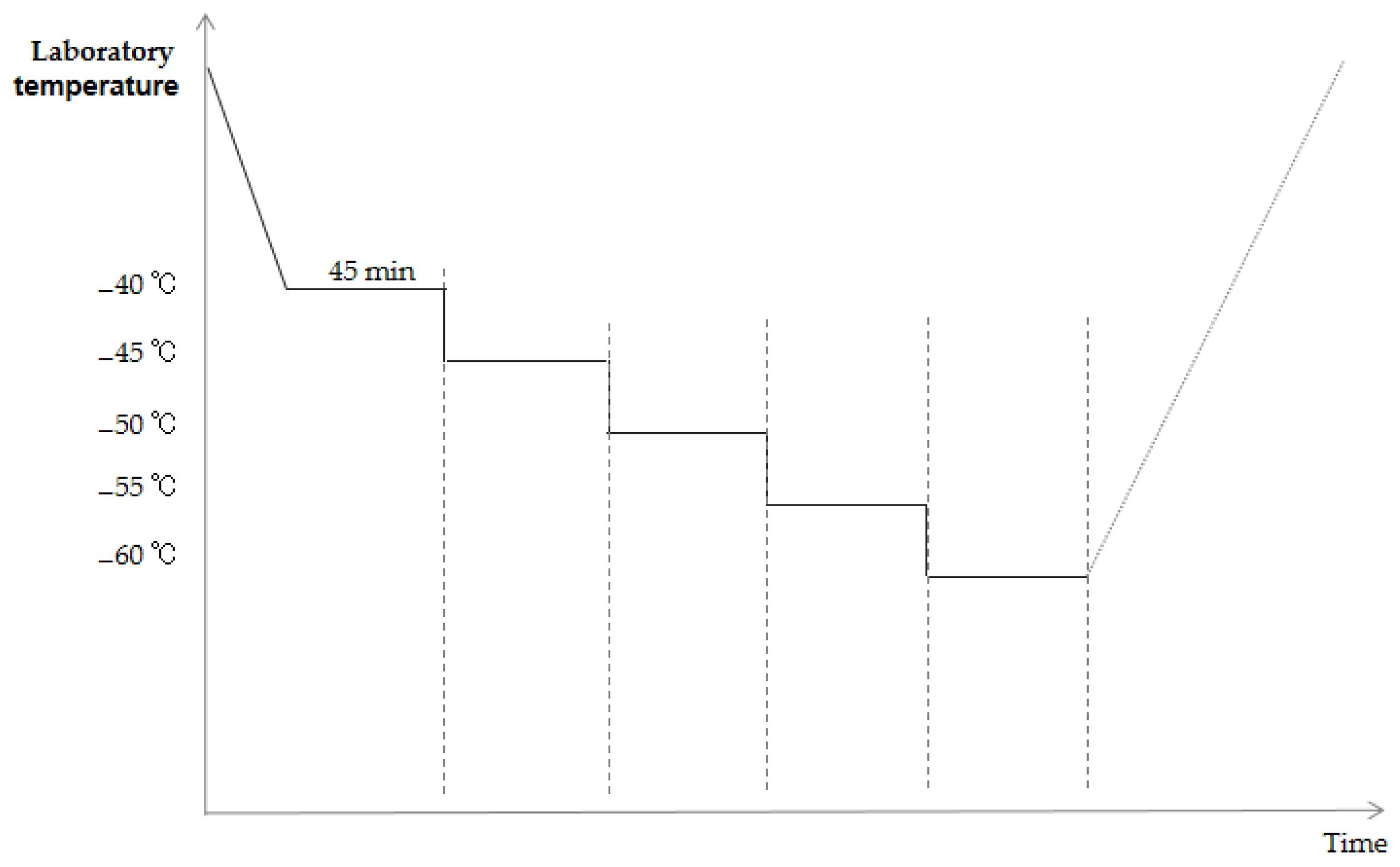
| 1 | Low-temperature step test | −70 °C | None | None |
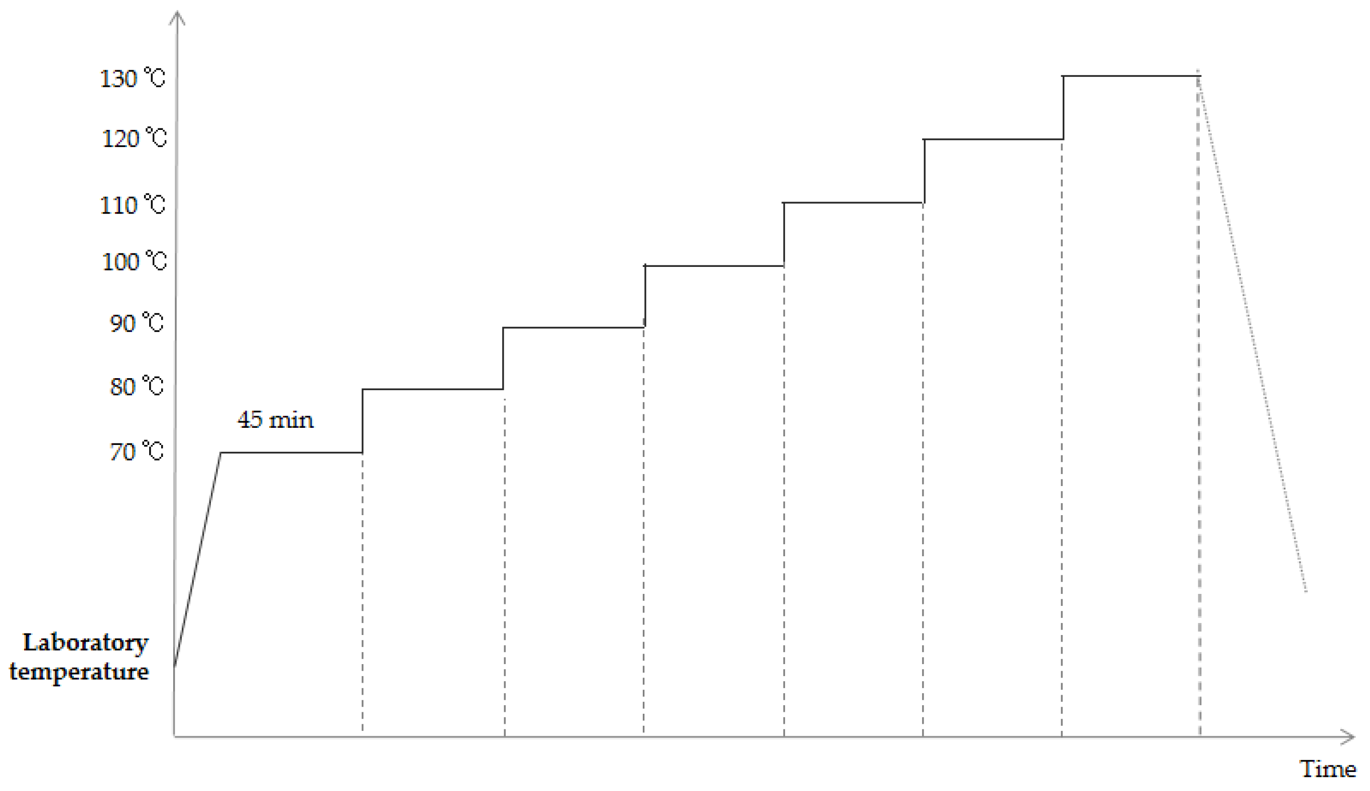
| 2 | High-temperature step test | High temperature step 1 (Max. 130 °C) | None | None |
| High temperature step 2 (Max. 270 °C) | At 230 °C, additional circuit failure occurs, and the number of circuit failures increases gradually with increasing temperature. | Short-circuit failure occurs at 270 °C | ||
| 3 | Rapid temperature change test | 60– 130 °C | Three new break failures | None |
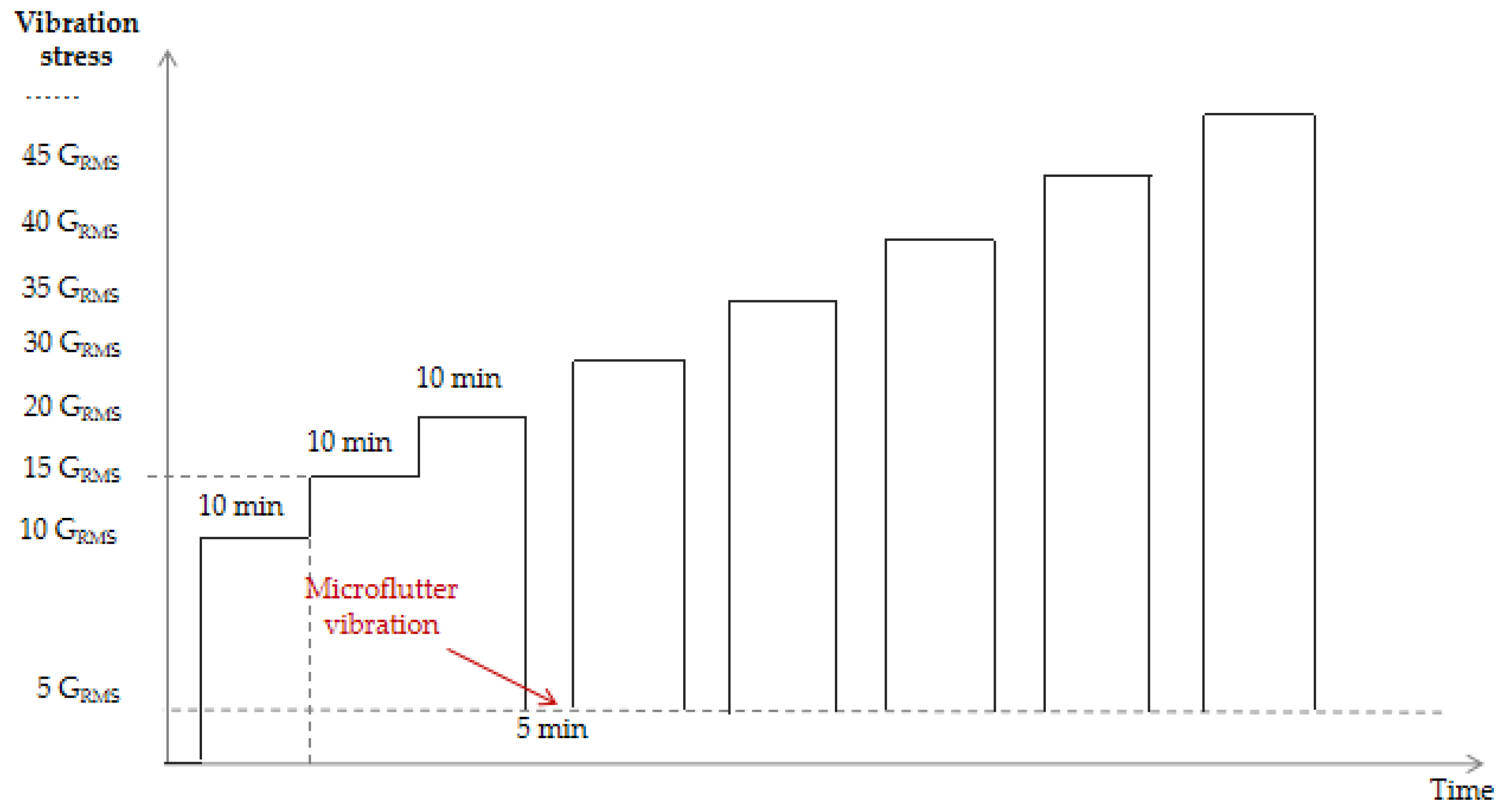
| 4 | Triaxial 6-DOF random vibration step stress test | 50 GRMS | Three new open-circuit failures, all occurring at matrix bit #5 | None |
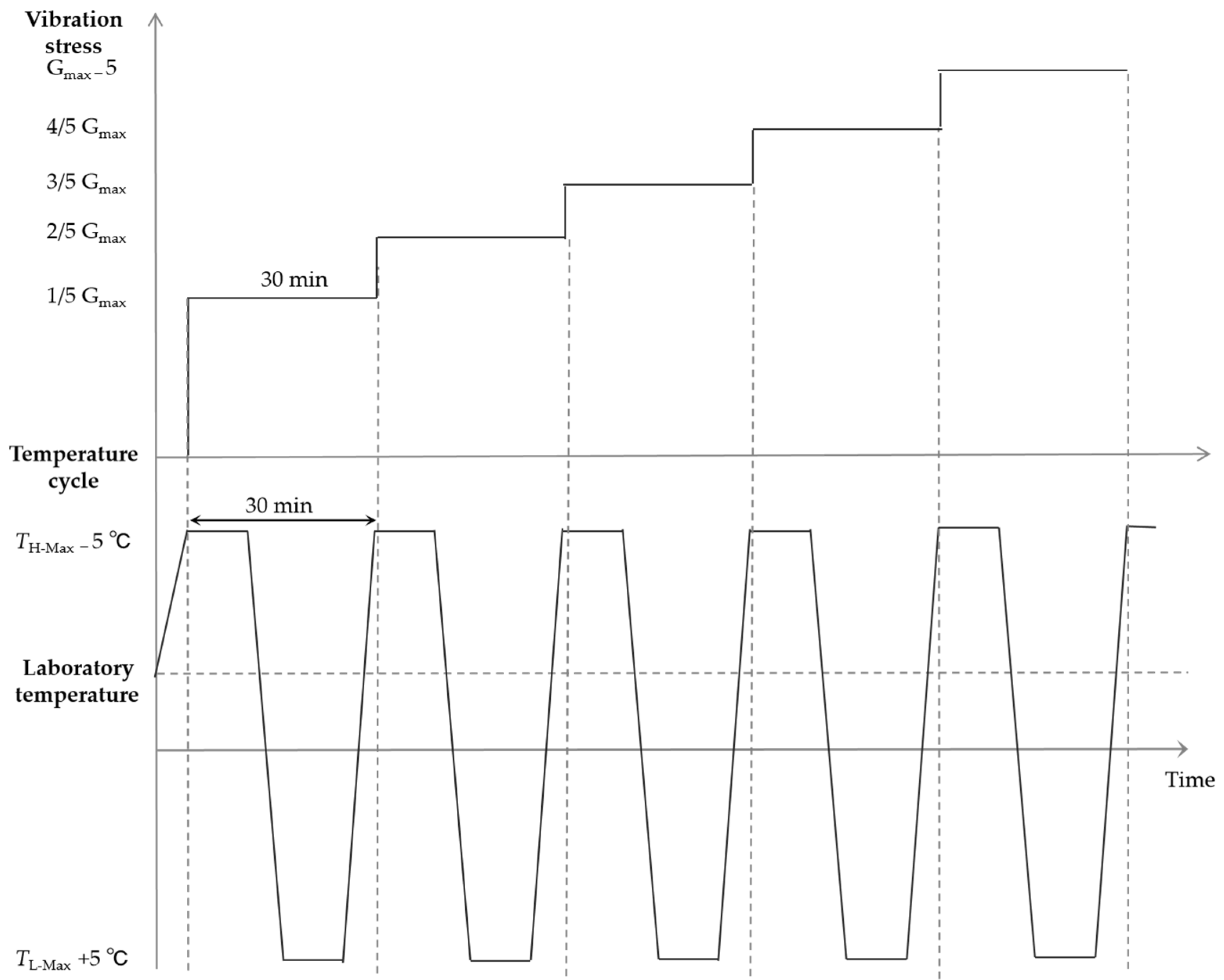
| 5 | Rapid temperature change + triaxial vibration comprehensive stress | 130 °C, 50 G | Five new circuit breaker failures, all occurring in E_z_5 | One short-circuit failure |
| 6 | High-temperature and high-humidity stress test | 90 °C, 100%RH | None | None |
| Serial Number | Diode New Failure Rate | |
|---|---|---|
| Open Circuit | Short Circuit | |
| 1 | 0% | 0% |
| 2 (step 1) | 0% | 0% |
| 2 (step 2) | 28.10% | 2.72% |
| 3 | 1.92% | 0% |
| 4 | 1.56% | 0% |
| 5 | 2.22% | 0.27% |
| 6 | 0% | 0% |
| Serial Number | Test Object | Test Items | Test Equipment | Purpose of Testing |
|---|---|---|---|---|
| 1 | Whole board | Visual inspection of appearance | Magnifying glass, stereomicroscope | Appearance of defects |
| 2 | X-ray detection | X-ray system | Observation of anomalies in the wiring | |
| 3 | C-SAM | Ultrasonic scanning microscope | Presence of voids, layering, etc., in the multilayer structure | |
| 4 | Diode | Visual inspection | Stereomicroscope | Appearance of defects |
| 5 | C-SAM | Ultrasonic scanning microscope | Scanning electron microscopy observations | |
| 6 | SEM and EDS analysis | Scanning electron microscope, energy dispersive X-ray spectroscopy instrument | Micromorphology observations, elemental composition analysis | |
| 7 | Slice analysis | Stereomicroscope, metallographic microscope, scanning electron microscope, energy dispersive X-ray spectroscopy instrument | Observation of the diode internal morphology, defect detection | |
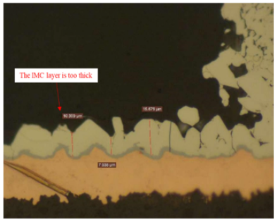
| 8 | Slice analysis | Solder joint analysis | Stereomicroscope, metallographic microscope, scanning electron microscope, energy dispersive X-ray spectroscopy instrument | Solder joint defect detection, IMC layer detection, analysis of harmful components |
| 9 | Line analysis | Stereomicroscope, metallographic microscope, scanning electron microscope, energy dispersive X-ray spectroscopy instrument | Circuit defect detection, analysis of harmful components | |
| 10 | Pad analysis | Stereomicroscope, metallographic microscope, scanning electron microscope, energy dispersive X-ray spectroscopy instrument | Analysis of the thickness and morphology of the pad coating | |
| 11 | Multilayer structure | Stereomicroscope | Observation of defects, such as delamination and voids |
| Failure Mode Number | Part | Failure Mode | Failure Mechanism | Test Results |
|---|---|---|---|---|
| 1 | PIN diode | Pole rupture resulting in diode breakdown and short-circuit failure | During vibration or thermal fatigue, pole rupture and breakdown take place, resulting in the formation of a short circuit. | Not found. |
| 2 | Inter-electrode solder melt adhesion and short-circuit failure | When the high temperature exceeds the melting point, the solder at both ends of the PIN diode dissolves, and the dissolution process leads to connection of the electrodes at the two ends, resulting in short-circuit failure. | 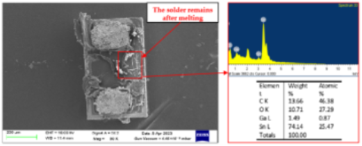 | |
| 3 | The electrode is broken at the bond of the tube core, and the circuit fails. | Under the action of vibration, thermal stress, etc., the bond between the electrode and the tube core may break, resulting in open-circuit failure of the PIN diode. | 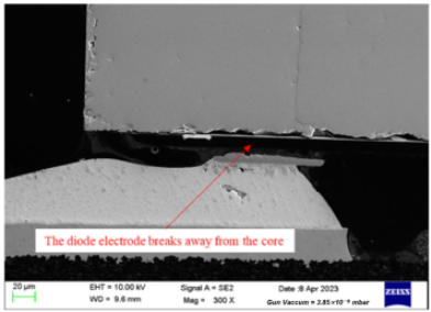 | |
| 4 | Body cracking and open-circuit failure | Random vibrations, temperature cycling, and high temperatures cause cracking of the PIN diode body. | 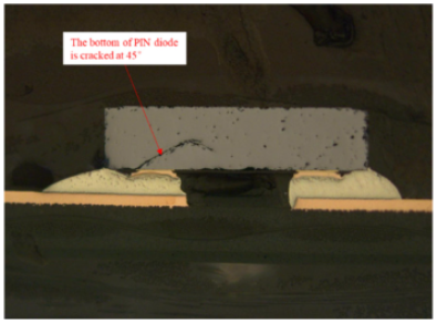 | |
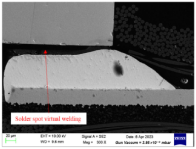
| 5 | Solder joint | Solder joint cavities |
| 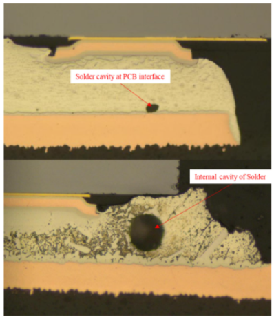 |
| 6 | Solder joint cracking |
|  | |
 | ||||
| Solder spot virtual welding |
|  | ||
| 7 | Inadequate solder melting | At high temperatures, secondary melting occurred, and an insufficient temperature led to a sword-like solder, coarse grains, and other phenomena. At this time, the solder joint strength is low, and it can easily crack or even fracture under the action of thermal and mechanical stresses. | 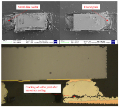 | |
| 8 | PCB | PCB substrate cracking |
The CTE describes the rate of change in length or volume per unit of a material in response to a change in temperature.
|  |
| 9 | Mask (green oil) peeling, cracking, and detachment |
|  | |
| 10 | Line oxidation | At high temperatures, the skin becomes unstuck, and a large area of discoloration was observed for the green oil, in addition to cracking and other phenomena. The protective effect of the line is greatly weakened, rendering the copper susceptible to oxidation at high temperatures. |  | |
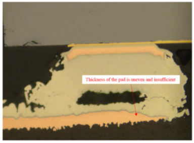
| 11 | Uneven and insufficient pad thickness |
|  | |
| 12 | Multilayer construction | Skin aging |
|  |
| 13 | Skin debonding |
| ||
| 14 | Bubbles are detected in the honeycomb structure | Bubbles introduced during the preparation process promote failure. | 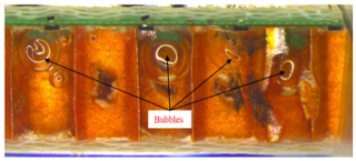 | |
| 15 | Bubbles are detected in the adhesive film | Bubbles that form during the preparation process can lead to failure. | 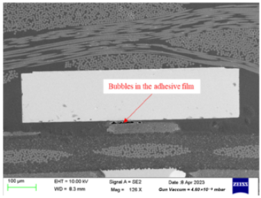 |
Disclaimer/Publisher’s Note: The statements, opinions and data contained in all publications are solely those of the individual author(s) and contributor(s) and not of MDPI and/or the editor(s). MDPI and/or the editor(s) disclaim responsibility for any injury to people or property resulting from any ideas, methods, instructions or products referred to in the content. |
© 2025 by the authors. Licensee MDPI, Basel, Switzerland. This article is an open access article distributed under the terms and conditions of the Creative Commons Attribution (CC BY) license (https://creativecommons.org/licenses/by/4.0/).
Share and Cite
Wei, Z.; Suo, B.; Zhou, C.; Li, Y.; Zhang, F. Research into the Failure Mechanism and Reliability of an Active Frequency-Selective Surface in Complex Environments. Materials 2025, 18, 1354. https://doi.org/10.3390/ma18061354
Wei Z, Suo B, Zhou C, Li Y, Zhang F. Research into the Failure Mechanism and Reliability of an Active Frequency-Selective Surface in Complex Environments. Materials. 2025; 18(6):1354. https://doi.org/10.3390/ma18061354
Chicago/Turabian StyleWei, Zheng, Bin Suo, Chunping Zhou, Yueqi Li, and Feng Zhang. 2025. "Research into the Failure Mechanism and Reliability of an Active Frequency-Selective Surface in Complex Environments" Materials 18, no. 6: 1354. https://doi.org/10.3390/ma18061354
APA StyleWei, Z., Suo, B., Zhou, C., Li, Y., & Zhang, F. (2025). Research into the Failure Mechanism and Reliability of an Active Frequency-Selective Surface in Complex Environments. Materials, 18(6), 1354. https://doi.org/10.3390/ma18061354