Article

Discovery of Room-Temperature Topological Insulators in Functionalized Group VA-VA Binary Monolayers: A First-Principles Investigation

National Graphene Research and Development Center, Springfield, VA 22151, USA
*
Author to whom correspondence should be addressed.
Materials 2025, 18(21), 5017; https://doi.org/10.3390/ma18215017
Submission received: 6 October 2025 / Revised: 26 October 2025 / Accepted: 27 October 2025 / Published: 4 November 2025

Abstract

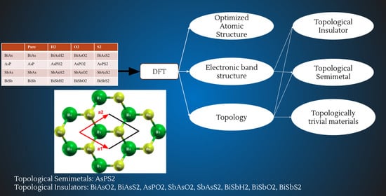
Topological insulators and semimetals are necessary to realize quantum computing and spintronics. We use first-principles calculations to investigate the atomic structure, electronic band structure, and Z2 invariants of four sets of pure and functionalized buckled hexagonal monolayers that are promising candidates for topological nature: BiAs, AsP, SbAs, BiSb, and functionalized monolayers BiAsX2, AsPX2, SbAsX2, and BiSbX2 (X = H, O, S). Our results show that BiAsO2, BiAsS2, AsPO2, SbAsO2, SbAsS2, BiSbH2, BiSbO2, and BiSbS2 are topological insulators with small SOC-induced band gaps ranging from 0.05 to 0.37 eV. Further, we propose AsPS2 to be a topological semiconductor. Topological insulators stand on the boundary of induction and conductance and are crucial in realizing quantum computers. The room-temperature topological insulators predicted here will have promising impacts in quantum computing, nanoelectronics, and spintronics.

Graphical Abstract

1. Introduction

Topological materials, specifically topological insulators (TIs) and topological semimetals (TSMs), have been shown to have novel surface states that are different from their bulk states [1]. TIs are known to be insulating in the bulk with gapless edge states [2] due to the inversion of the conduction and valence bands by strong spin orbit coupling (SOC) [3]. These surface states have spin-momentum locking, which allows for exotic electron transport properties [4] and makes TIs valuable in spintronics. TIs are also valuable in thermoelectrics for their unique combination of an insulating bulk with conducting surface states. In the past decade, there has been an explosion of research into new TSMs and identifying and categorizing TSMs into Dirac, Weyl, and many other categories [5,6]. TSMs show great potential for quantum computing [7] and spintronics [8]. TIs and TSMs both have robust boundary states resistant to perturbations [9], which is crucial for protecting delicate quantum systems from unwanted noise.
Many materials have been theorized to be TIs, but few have been confirmed experimentally. The first TI was the CdTe/HgTe/CdTe quantum well [10,11], which consisted of a thin layer of HgTe between two layers of CdTe. Soon after, the first 3D TI was experimentally confirmed: Bi1−xSbx [10,12,13]. Well-known 3D TIs include Bi2Se3, Bi2Te3, and Sb2Te3 [2,12]. However, 3D TIs are relatively difficult to use in spintronics and other applications due to degradation when scaled down [14], and thus researchers have shifted their focus to 2D topological materials candidates. Theoretically predicted and experimentally verified 2D TIs include bismuthene [15,16] and Na3Bi [15,17], which have the largest topological gaps to date [15]. Recently, research has been focused on searching for room-temperature 2D TIs, which are crucial for room-temperature spintronics [18]. Additionally, the edge states of 2D TIs are one of the few places that Majorana fermions, crucial to quantum computing, can be observed [19].
In past decades, 2D monolayer topological material candidates have been the center of investigations both theoretically and experimentally. Single-element monolayer TIs include arsenene [6], antimonene [6], silicene [20], germanene [15,20,21], and stanene [20], which have all been experimentally confirmed. Multi-element monolayer TIs include the aforementioned bismuthene [15,16]. In particular, 2D binary monolayers are gaining attention, such as the experimentally confirmed group IIIA-VA binary monolayers GaBi, InBi, TlBi, TlAs, TlSb, and TlN [22]. However, these materials have small band gaps that are not significant at room temperature, necessitating further research for room-temperature TIs.
Most recently, the Group-VA family has attracted interest for their variety of allotropes with properties that make them suitable for electronics, spintronics, and energy devices [6]. 2D VA-VA binary monolayers have attracted great attention for their stable structure and material properties [23,24,25,26,27,28,29,30,31,32,33]. The buckled honeycomb structures of BiAs, AsP, SbAs, and BiSb have all already been investigated for topological nature, with BiAs, SbAs, and BiSb all being strain-induced TIs [34,35,36]. We will briefly describe our reproduction of the results published in previous literature in Section 3.1. We did not calculate strain effects. Additionally, functionalization of binary monolayers is a well-known method for creating a topological phase transition [37].
To date, there is still a gap in the research of room-temperature topological insulators. We dive in to provide insight into room-temperature topological insulator candidates by pursuing functionalized Group VA-VA monolayers in order to realize a new direction for topological materials research. Our focus is on investigating: BiAs and functionalized BiAsX2 (X = H, O, S); AsP and functionalized AsPX2 (X = H, O, S); SbAs and functionalized SbAsX2 (X = H, O, S); and BiSb and functionalized BiSbX2 (X = H, O, S) for their atomic structure, electronic properties, and topological nature. We have reproduced pure BiAs, AsP, SbAs, and BiSb to prove the validity of our method. The novelty of our research is in the functionalized BiAsX2, AsPX2, SbAsX2, and BiSbX2 (X = H, O, S).
In Section 2, we detailed our methods to perform first-principles calculations. In Section 3, we present our results. We discuss and compare our results with other theoretical research in Section 3.1. Finally, our conclusion and directions for future research are found in Section 4.

2. Materials and Methods

We performed first-principles calculations based on Density Functional Theory (DFT) within the Generalized Gradient Approximation (GGA) in Perdew-Burke-Ernzerhof (PBE) format implemented in the ABINIT [38] 9.8.4 code. We use the Projector Augmented Wave (PAW) method to generate [39] pseudopotentials with the ATOMPAW 4.0.0.12 code [40]. Scalar-relativistic PAW pseudopotentials were used in all calculations. The electron configurations and radius cutoffs of the atoms used in current calculations are listed in Table 1.
Total energy calculations using self-consistent field (SCF) iterations were considered converged when the difference in total energy between two adjacent iterations was less than 1.0 × 10 10 Ha twice consecutively. The kinetic energy cutoff, Monkhorst-Pack k-point grid, and vacuum height were considered converged when the total energy difference between two neighboring datasets was lower than 1.0 × 10 4 Ha twice. These convergence criteria have been used in previous research [10,41] and proven to be reliable. The converged values for each structure are listed in Table 2.
The Broyden–Fletcher–Goldfarb–Shanno (BFGS) minimization algorithm was used for structural optimization. Each structure was considered fully relaxed once the maximum forces were less than 1.0 × 10 5 Ha/Bohr.
The electronic structures of each material were analyzed through band structure and fatband structure calculations. All band structure calculations were carried out using the following high-symmetry k-point circuit in the irreducible first Brillouin zone: Γ (0.0, 0.0, 0.0) → K (1/3, 2/3, 0.0) → M (1/2, 1/2, 0.0) → Γ (0.0, 0.0, 0.0).
We used the Wannier90 [42] 3.1.0 software package to track the evolution of the hybrid Wannier charge centers (HWCC), which has been used frequently and proven reliable in previous literature [10,41]. We used the Z2Pack [43,44] 2.2.1 software package to determine the Z2 invariant.
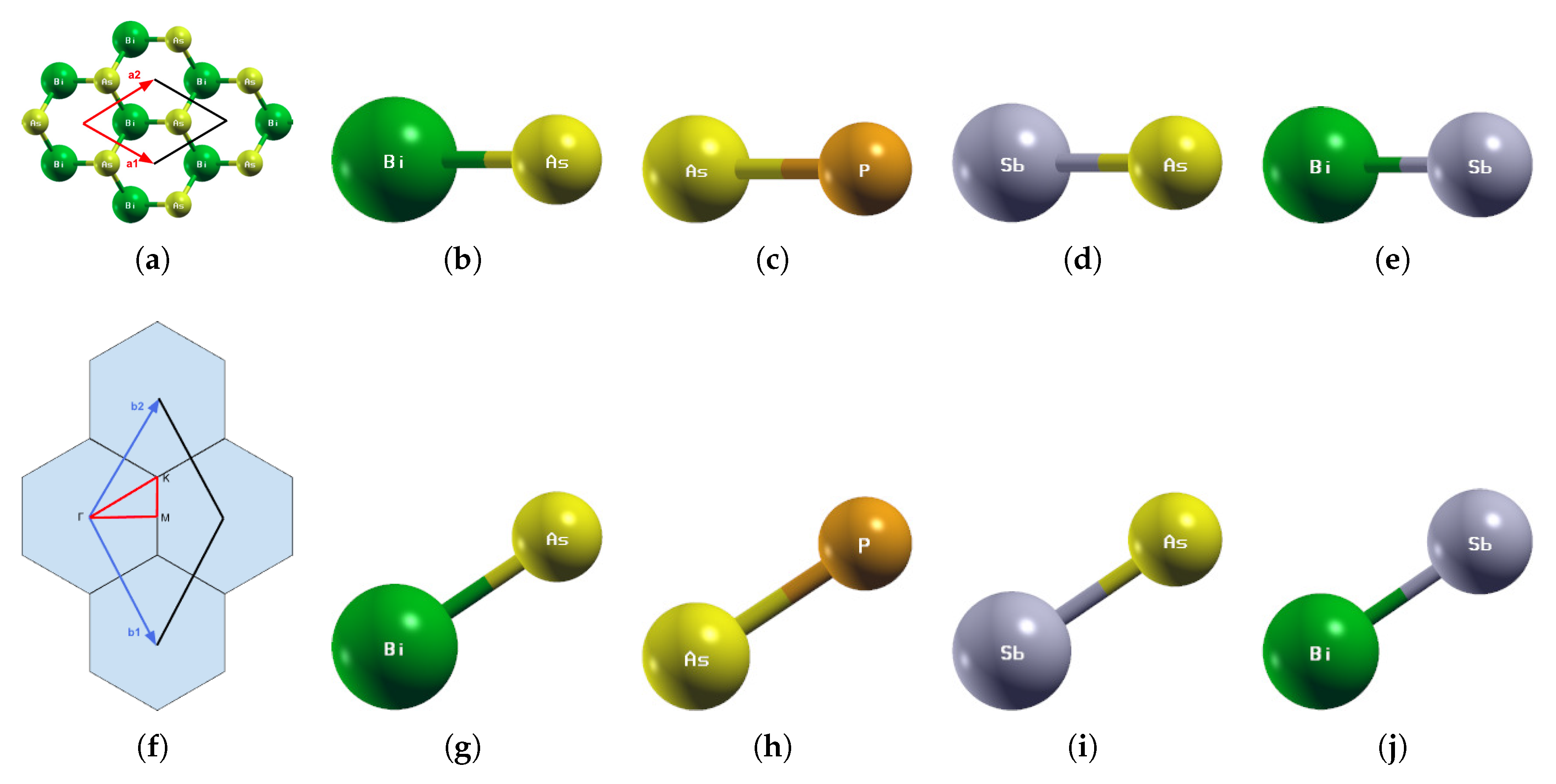
Our calculations are first-principle calculations, so no parameters were involved. The input data consists only of the atomic pseudopotentials and the lattice structure. We used the pure materials BiAs, AsP, SbAs, and BiSb to prove the validity of our methodology, which serves as justification for the reliability of our other results and provides reproducibility (Figure 1).

3. Results and Discussion

We investigated Group-VA monolayers BiAs, AsP, SbAs, and BiSb, as well as functionalized monolayers BiAsX2, AsPX2, SbAsX2, BiSbX2 (X = H, O, S).
We calculated the optimized atomic structure, the band structures with and without SOC, the fatbands, and the Z2 invariant.

3.1. Pure BiAs, AsP, SbAs, BiSb

The optimized atomic structures of pure BiAs, AsP, SbAs, and BiSb are shown in Figure 2. All four monolayers are buckled honeycomb structures, similar to Boron Nitride from a top view but appearing as a zigzag pattern from the side view. Each structure has two atoms per unit cell. The lattice parameters of the above four pure monolayers are listed in Table 3. The current lattice constants and buckling heights are consistent with previous first-principles calculations [24,28,31,35,45,46,47,48].
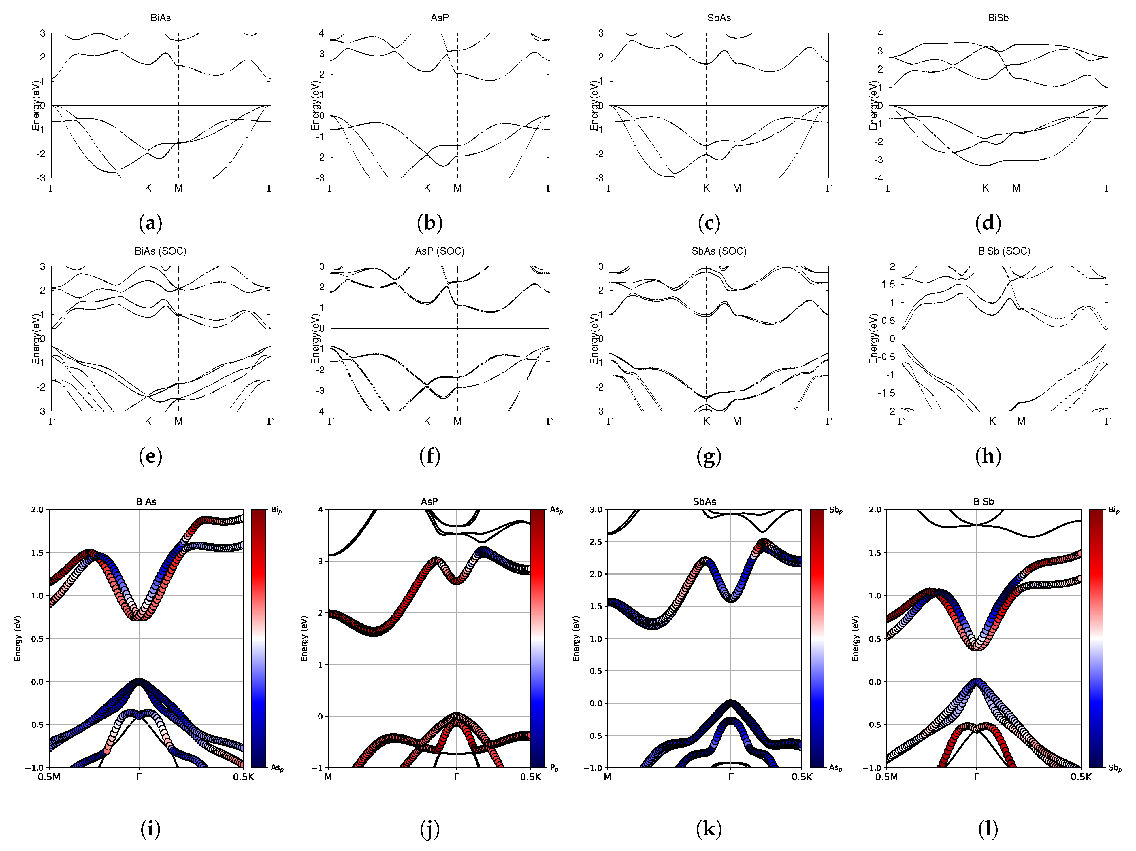
The electronic band structures are clearly displayed in Figure 3. As shown in the first and second rows of Figure 3, all four materials have their valence band maximum (VBM) at the Γ point, both with and without SOC effects. All four electronic band structures show double degeneracies in both the valence and conduction band at the Γ high-symmetry point with SOC. BiAs has a direct band gap at Γ , and an indirect band gap with SOC due to band splitting. In BiAs, we have calculated a band gap of 0.75 eV, comparable to the previously calculated value of 0.70 eV [45]. AsP has conduction band minimum CBM between the M and Γ points both with and without SOC, as shown in Figure 3a,e. AsP has an indirect band gap of 1.70 eV, which is smaller than the previously calculated value of 1.82 eV [46]. The difference may be due to the semi-empirical DFT-D2 correction scheme used in previous calculations [46]. Similarly to AsP, SbAs has CBM between the M and Γ points both with and without SOC, as shown in Figure 3c,g. SbAs has an indirect band gap of 1.39 eV, and 1.20 eV with SOC, which is comparable to previous calculated values of 1.47 eV and 1.27 eV with SOC [35]. In BiSb, we have calculated a band gap with and without SOC of 0.40 and 1.00 eV, comparable to previously calculated values of 0.37 [47] and 0.36 eV [48] with SOC and 0.95 [47] and 0.96 eV [48] without SOC.
It is well known that larger atoms, especially Bismuth, will show stronger SOC effects [49]. The current calculation found that molecular structures with higher atomic mass experienced greater SOC effects (SOC reduces the band gap of BiSb by 0.60 eV, compared to a 0.09 eV band gap reduction for AsP), as shown in Table 3.
Investigating the fatbands in the third row of Figure 3, BiAs seems to have some inversion, especially in the conduction bands. The valence bands are dominated by As-4p orbitals, with some influence from Bi-6p orbitals. AsP has valence bands and CBM entirely dominated by the As-4p orbitals, as shown in Figure 3j and does not show significant band inversion. SbAs also has valence bands and CBM entirely dominated by As-4p orbitals, as shown in Figure 3k, and does not show significant band inversion. BiSb seems to have some inversion, similar to BiAs. The valence bands change from 6p orbital dominated to 5p orbital dominated around the Γ point.
All four band structures are in agreement with previous literature [25,35,45,47,48], which confirms the validity of our band structures.
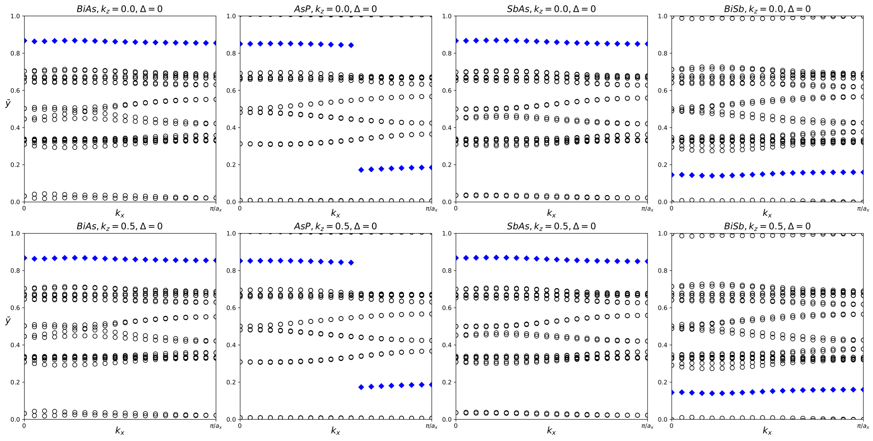
Although none of the four fatbands show clear band inversion, it is still worthwhile to investigate their Z2 indices. Tracking the movement of the Hybrid Wannier Change Centers reveals that all four pure structures have Z2 = 0, as displayed in Table 3 and Figure 4.
As previously stated in Section 1, BiAs, SbAs, and BiSb are already proven to be strain-induced topological insulators [34,35,36]. Our calculations of BiAs, AsP, SbAs, and BiSb are carried out at 0 pressure to replicate former work and show that our methodology produces results in agreement with previous literature.

3.2. BiAsX2 (X = H, O, S)

The optimized atomic structures of BiAsX2 (X = H, O, S) are shown in Figure 5. All four monolayers are buckled honeycomb structures, appearing as a zigzag pattern from the side view. Each structure has four atoms per unit cell. The lattice constants, buckling heights, and electronic band structures of the functionalized BiAsX2 monolayers are shown in Table 4 and Figure 6.
Notably, the side view of BiAs2 as shown in Figure 5d reveals that BiAsH2 buckles inwards rather than outwards like BiAsO2 and BiAsS2. BiAsH2 also has an extremely small buckling height of 0.04Å compared to 0.96 Å for BiAsO2 and 1.15 Å for BiAsS2.
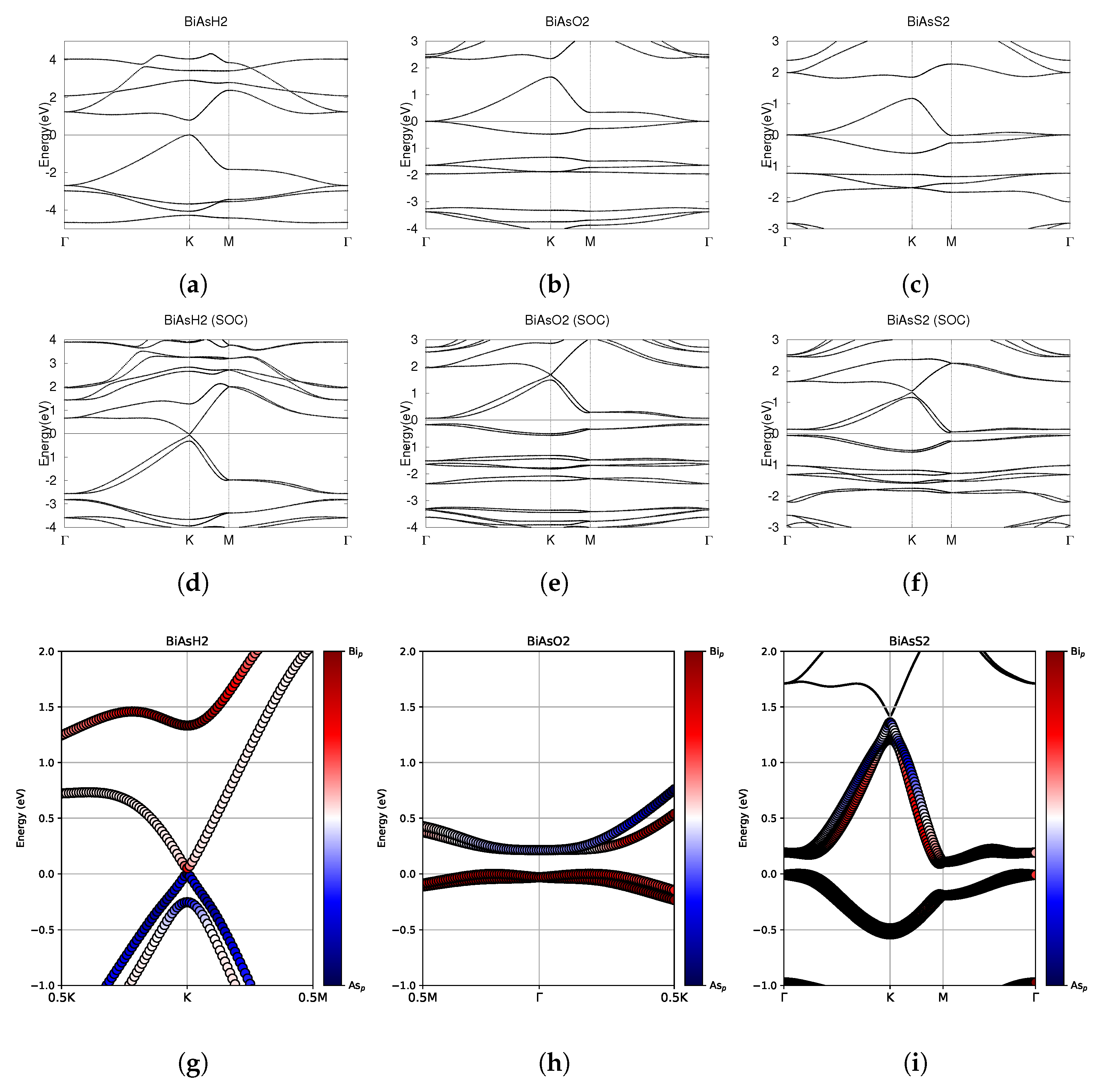
The band structure without and with SOC, as well as the fatbands, are shown in Figure 6. BiAsH2 is a semiconductor with a direct band gap of 0.79 eV at the K point. BiAsH2 uniquely experiences very strong SOC in the conduction band. The VBM and CBM do not become degenerate at the K point with or without SOC. There is a very small but nonzero direct band gap of 0.05 eV with SOC, as noted in Table 4. Figure 6b shows that BiAsO2 has CBM and VBM degenerate at the Γ point, forming a Dirac point. As shown in Figure 6c, the CBM of BiAsS2 is at the M point and is below the VBM, suggesting that BiAsS2 is semimetallic. In both BiAsO2 and BiAsS2, SOC effects break the degeneracy at the Γ point, which is a well known indicator of significant topological nature. After SOC, BiAsO2 has an indirect band gap of 0.21 eV, and BiAsS2 has an indirect band gap of 0.09 eV.
Investigating the fatbands in the third row of Figure 6, BiAsH2 shows little evidence of band inversion. The conduction bands of BiAsH2 are entirely dominated by Bi-6p orbitals and the valence bands are solely dominated by As-4p orbitals. The bands around the fermi level in BiAsO2 and BiAsS2 seem to be largely dominated by the Bi-6p orbitals, with one conduction band in both BiAsO2 and BiAsS2 being dominated by As-4p orbitals.
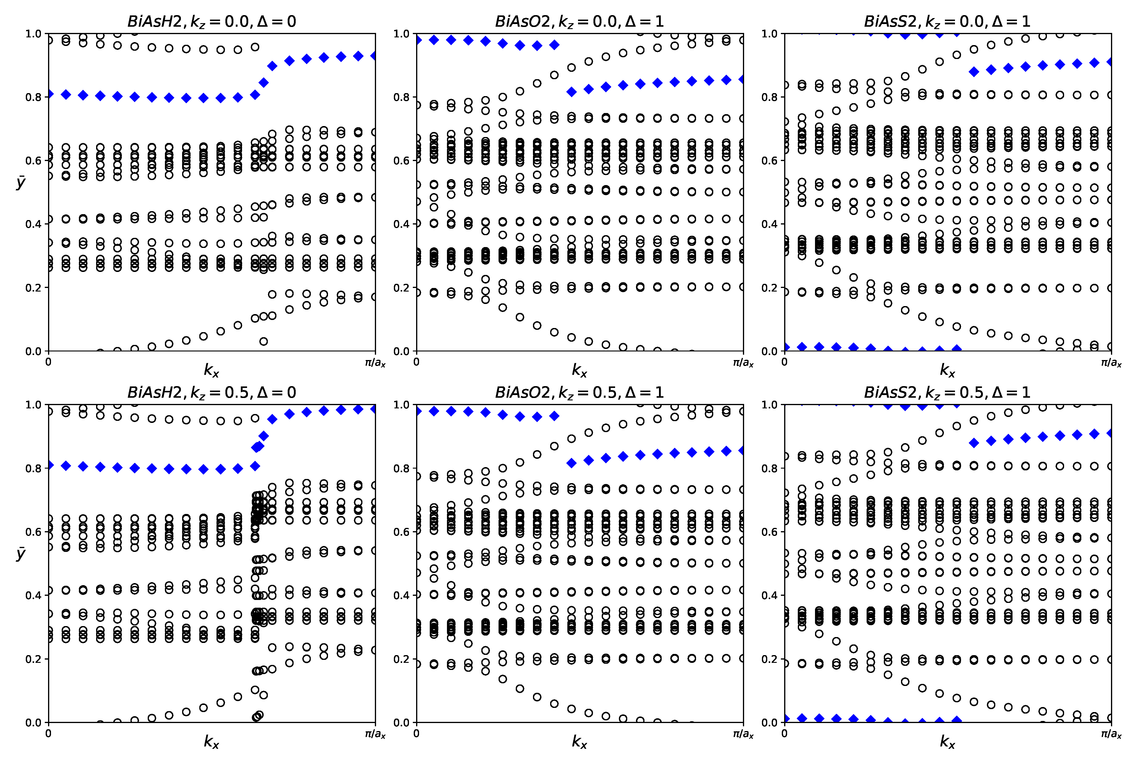
Although the fatbands for BiAsO2 and BiAsS2 appear to lack band inversion, it is still worthwhile to examine the Z2 indices of all three materials. The results of tracking the evolution of the hybrid Wannier charge centers are shown in Figure 7. BiAsH2 has Z2 = 0, indicating trivial topology. BiAsO2 and BiAsS2 both have Z2 = 1, which confirms that both materials are topologically nontrivial.
BiAsH2 is a trivial semiconductor, while BiAsO2 and BiAsS2 are small band gap topological insulators.

3.3. AsPX2 (X = H, O, S)

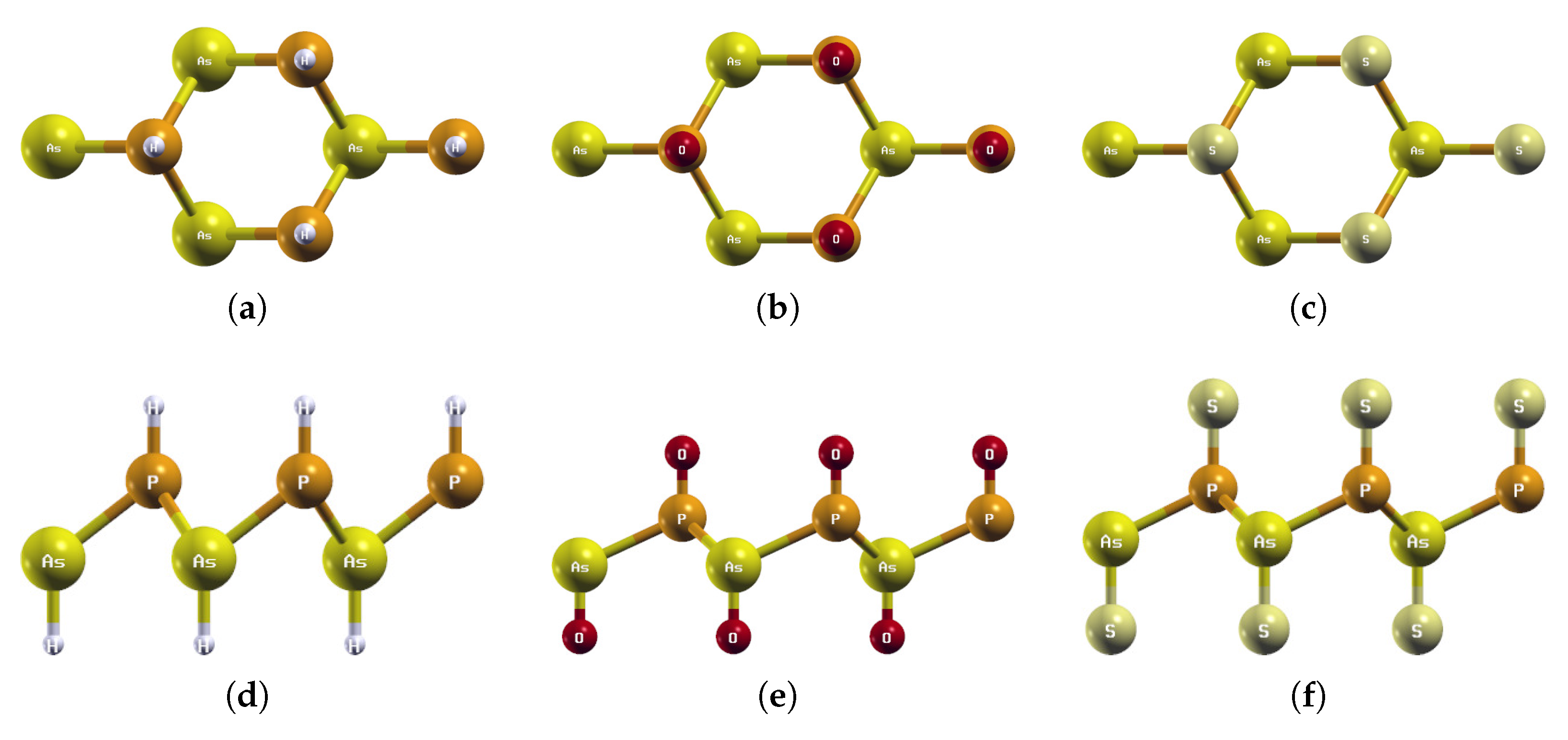
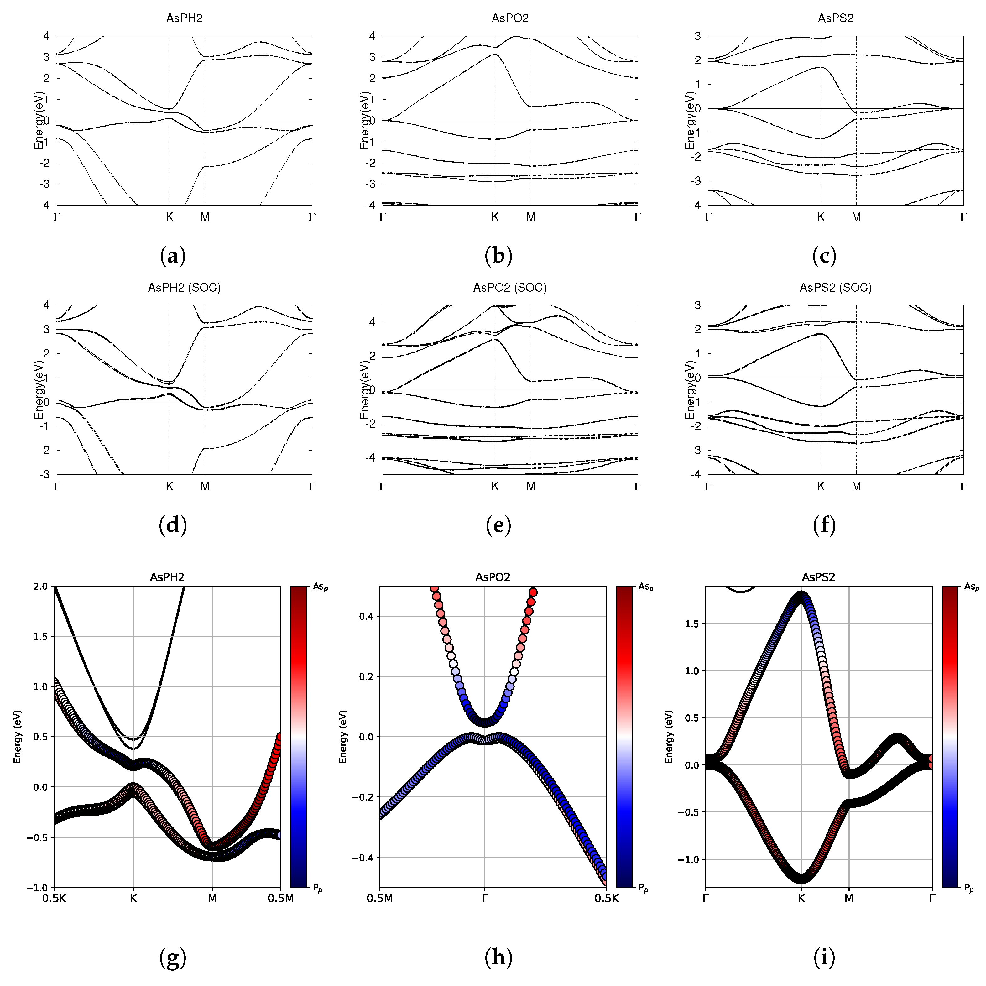
The optimized atomic structures of AsPX2 (X = H, O, S) are shown in Figure 8. All four monolayers are buckled honeycomb structures, appearing as a zigzag pattern from the side view. Each structure has four atoms per unit cell. The lattice constants, buckling heights, and electronic band structures of the functionalized AsPX2 monolayers are shown in Table 5 and Figure 9.
As shown in Figure 8, AsPH2 buckles outwards like AsPO2 and AsPS2. AsPH2 has a relatively large buckling height of 1.54 Å, compared to 1.09 Å for AsPO2 and 1.15 Å for AsPS2. Among all four H2-functionalized monolayers, AsPH2 is the only structure to buckle outwards. BiAsH2 has already been discussed in Section 3.2. SbAsH2 and BiSbH2 will be discussed later in Section 3.4 and Section 3.5, and are shown to buckle inwards in Figures 11d and 14d.
Investigating the electronic band structure, Figure 9a shows that AsPH2 has a negative indirect band gap, suggesting a semimetallic nature. Both with and without SOC, the CBM is at the M point and the VBM is at the K point. As shown in Figure 9b, AsPO2 has a Dirac point at the Γ point. When including SOC effects, the degeneracy at the Γ point is broken, indicating significant topology. After SOC, AsPO2 has a small indirect band gap of 0.05 eV. Figure 9c reveals that AsPS2 has a band crossing at the Γ point. The CBM is at the M point and crosses the Fermi level. The indirect negative band gap suggests that AsPS2 is a semimetal. Similarly to AsPO2, SOC breaks the degeneracy at the Γ point, indicating significant topological nature.
Investigating the fatbands in the third row of Figure 9, AsPH2 shows little evidence of band inversion. The fatbands for AsPO2 suggest possible band inversion, with the conduction band changing from being largely dominated by the As-4p orbital to the P-3p orbital. AsPS2 is largely dominated by As-4p orbitals. The conduction band is dominated by the P-3p orbitals at high energy levels.
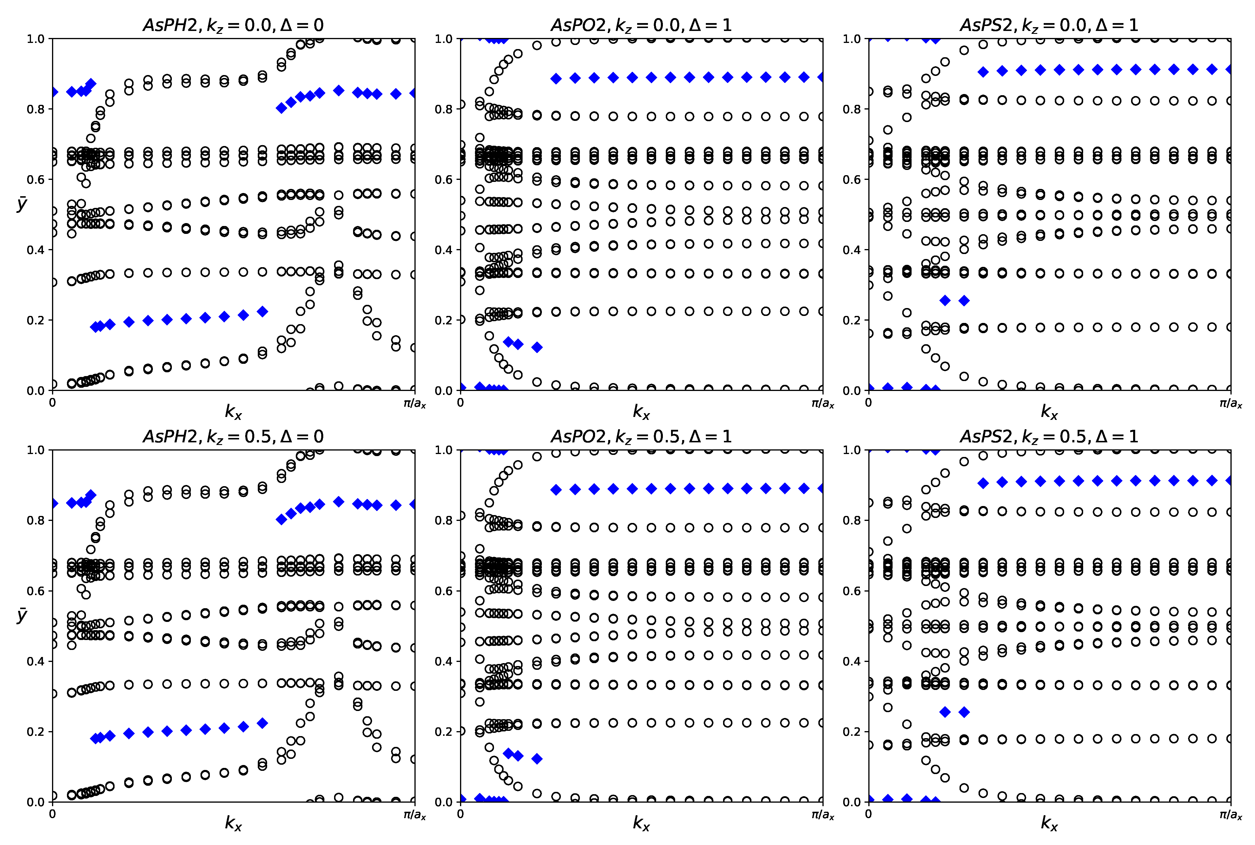
Despite no conclusive evidence of band inversion in the fatbands, it is still worthwhile to investigate the z2 indices of all three structures. The evolution of the hybrid Wannier charge centers and the Z2 invariant are shown in Figure 10. The Z2 indices are also listed in Table 5. AsPH2 has Z2 = 0, indicating trivial topology. AsPO2 and AsPS2 both have Z2 = 1, indicating nontrivial topology.
AsPH2 is a trivial semiconductor, AsPO2 is a small band gap topological insulator, and AsPS2 is a topological semimetal.

3.4. SbAsX2 (X = H, O, S)

The optimized atomic structures of SbAsX2 (X = H, O, S) are shown in Figure 11. All four monolayers are buckled honeycomb structures, appearing as a zigzag pattern from the side view. Each structure has four atoms per unit cell. The lattice constants, buckling heights, and electronic band structures of the functionalized SbAsX2 monolayers are shown in Table 6 and Figure 12.
As shown in Figure 11a, SbAsH2 buckles inwards. SbAsO2 and SbAsS2 buckle outwards. Similarly to BiAsH2, SbAsH2 has a very small buckling height of 0.06 Å compared to 1.05 Å for SbAsO2 and 1.20 Å for SbAsS2, as listed in Table 6.
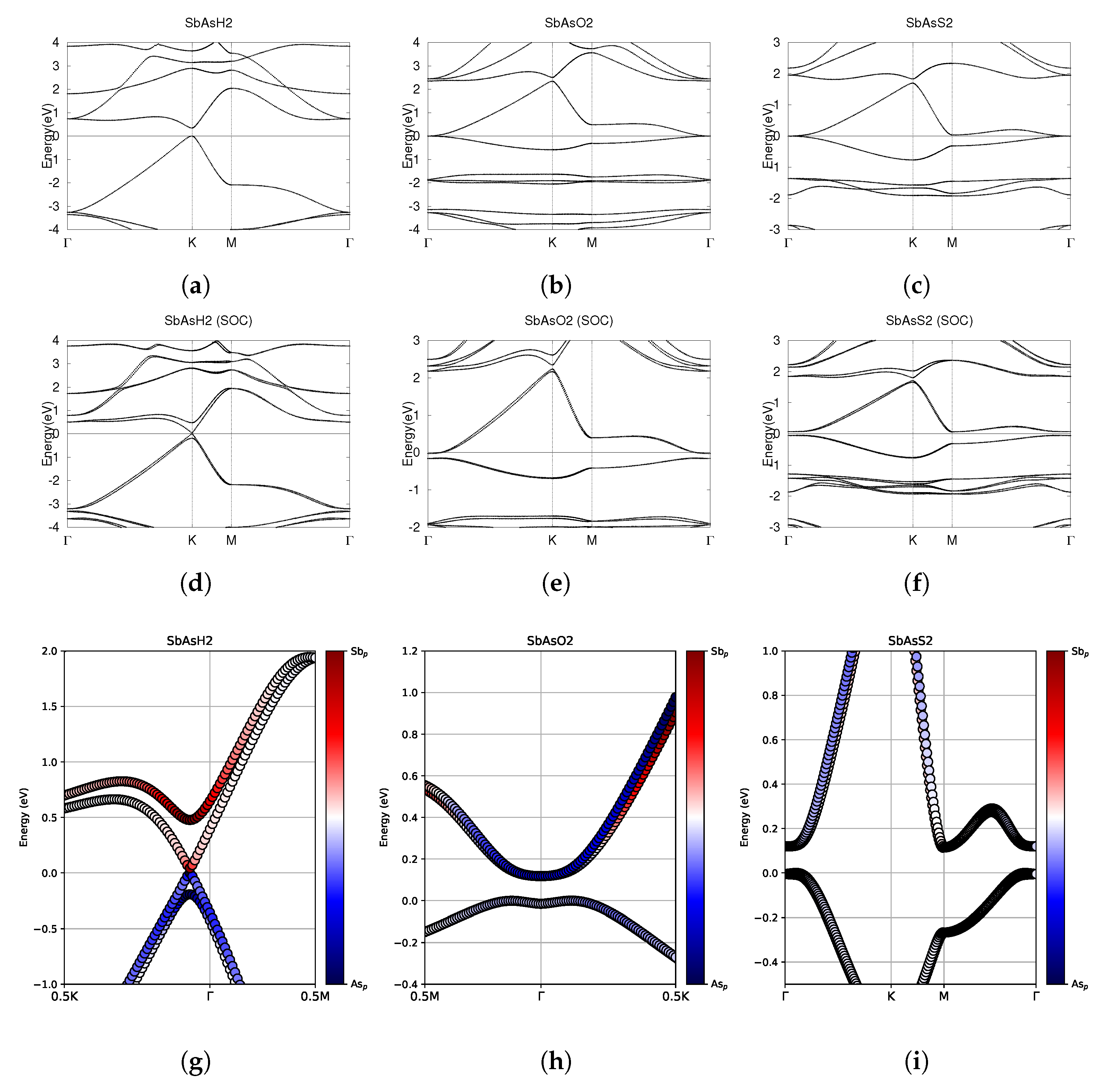
Investigating the electronic band structure, Figure 12a,d reveals that SbAsH2 has a direct band gap at the K point both with and without SOC. Without SOC, SbAsH2 has a band gap of 0.35 eV. Similarly to BiAsH2 as shown in Figure 6a,d, SOC-induced spin splitting in the conduction band reduces the band gap of SbAsH2 to a very small value of 0.04 eV. SbAsO2 has CBM and VBM degenerate at the Γ point, forming a Dirac point. Including SOC effects breaks the degeneracy at Γ , indicating significant topological nature. With SOC, the conduction bands are twofold degenerate at the Γ point, as shown in Figure 12b. The valence bands are also twofold degenerate at the Γ point. After SOC, SbAsO2 has an indirect band gap of 0.12 eV, as listed in Table 6 and shown in Figure 12e. As shown in Figure 12c, SbAsS2 has CBM crossing the Fermi level at the M point. The conduction and valence bands are degenerate at the Γ point. This degeneracy is broken by SOC effects, suggesting significant topology. SOC effects create an indirect band gap of 0.11 eV. After SOC, the CBM stays at the M point, but no longer crosses the fermi level.
Investigating the fatbands in the third row of Figure 12, SbAsH2 clearly has no band inversion, similarly to BiAsH2 in Figure 6g. Figure 12g shows that the conduction bands are dominated entirely by Sb-5p orbitals. The valence bands are dominated solely by As-4p orbitals. SbAsO2 has some orbital mixing, as shown in Figure 12h. The lowest conduction band is largely dominated by Sb-5p orbitals, but is dominated by As-4p orbitals around the Γ point. As shown in Figure 12i, the fatbands of SbAsS2 around the fermi level are not dominated by either p orbital. The lower conduction band is dominated by Sb-5p orbitals at high energy levels. The upper conduction band is dominated by As-4p orbitals at high energy levels.
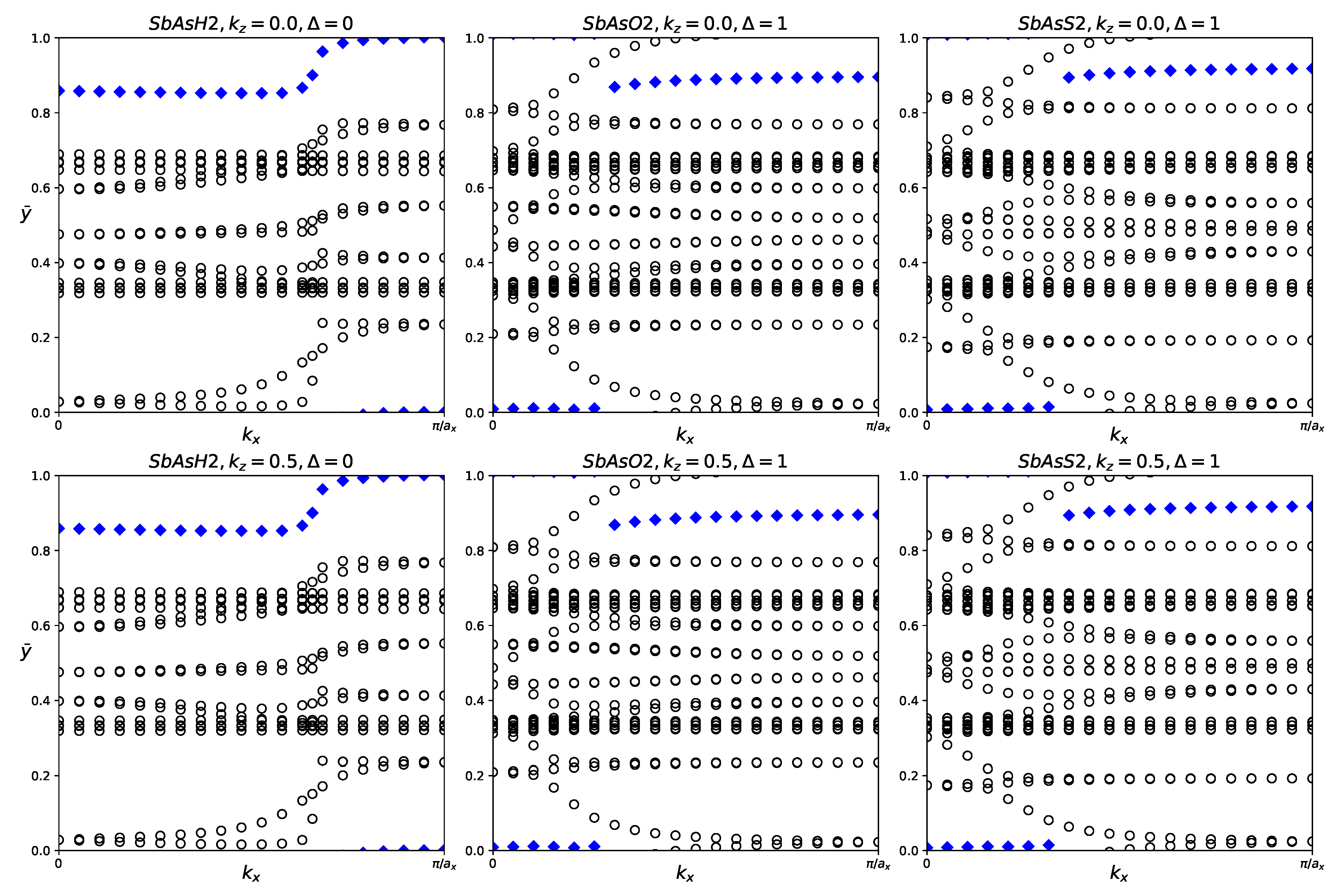
For each structure, we calculated the Z2 invariant by tracking the evolution of the hybrid Wannier charge centers, as shown in Figure 13. Indeed, SbAsH2 does not have significant topological nature. SbAsO2 and SbAsS2 were calculated to have Z2 = 1, indicating nontrivial topology.
SbAsH2 is a trivial semiconductor. SbAsO2 and SbAsS2 are small band gap topological insulators.

3.5. BiSbX2 (X = H, O, S)

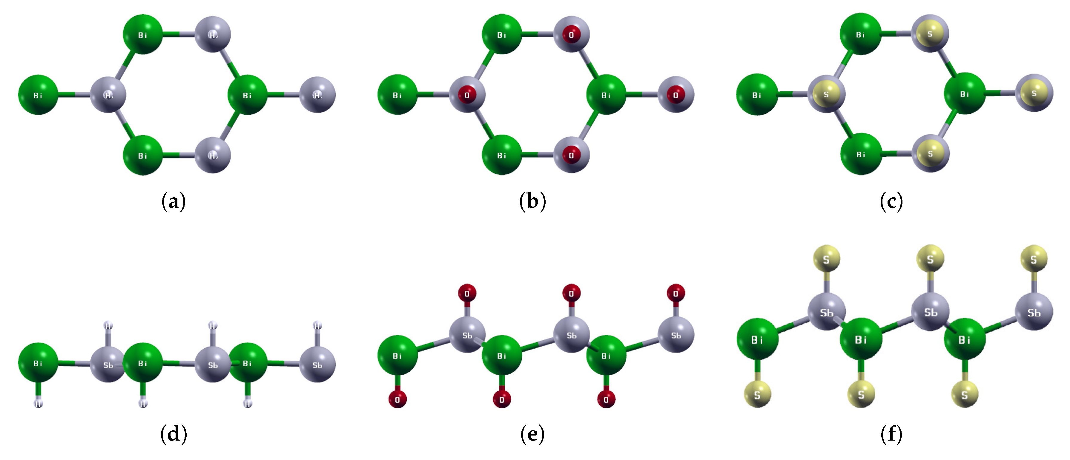
The optimized atomic structures of BiSbX2 (X = H, O, S) are shown in Figure 14. All four monolayers are buckled honeycomb structures, appearing as a zigzag pattern from the side view. Each structure has four atoms per unit cell. The lattice constants, buckling heights, and electronic band structures of the functionalized BiSbX2 monolayers are shown in Table 7 and Figure 15.
As shown in Figure 14d, BiSbH2 buckles inwards. BiSbO2 and BiSbS2 buckle outwards. Similarly to BiAsH2 and SbAsH2 discussed previously, BiSbH2 has a very small buckling height of 0.08 Å compared to 0.91 Å for BiSbO2 and 1.16 Å for BiSbS2, as listed in Table 7.
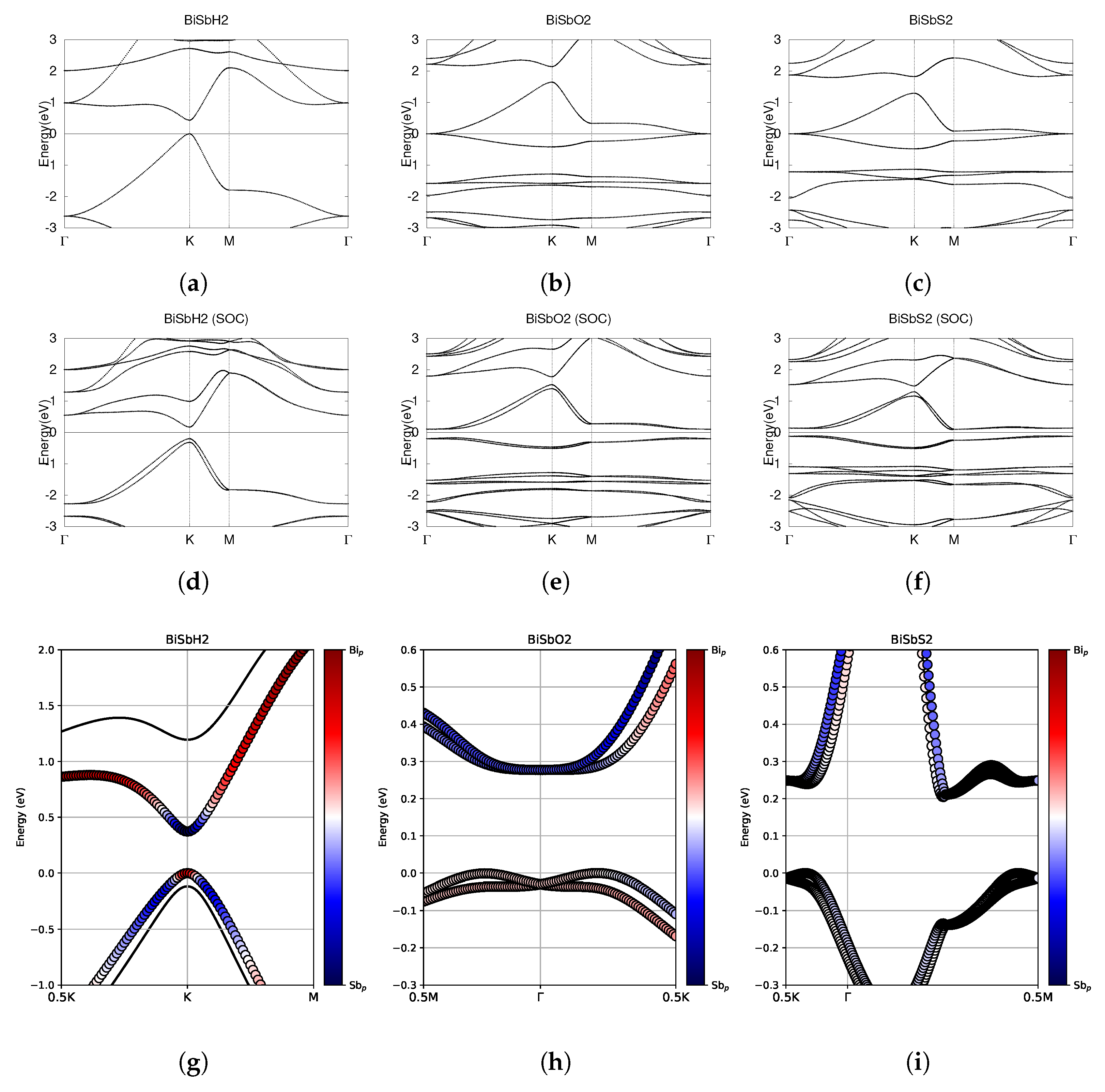
Investigating the electronic band structure, Figure 15a,d reveals that BiSbH2 has a direct band gap at the K point both with and without SOC. Before SOC, BiSbH2 has a band gap of 0.43 eV. After SOC, the band gap is reduced to 0.37 eV. BiSbO2 has VBM and CBM degenerate at the Γ point, forming a Dirac point. SOC effects breaks the degeneracy at Γ , indicating significant topological nature. With SOC, the conduction bands are twofold degenerate at the Γ point, as shown in Figure 15e and with greater detail in Figure 15h. The valence bands are also twofold degenerate at the Γ point. After SOC, BiSbO2 has an indirect band gap of 0.28 eV, as listed in Table 7. As shown in Figure 15c, BiSbS2 has VBM and CBM degenerate at the Γ point, forming a Dirac point. SOC effects breaks the degeneracy at Γ , indicating significant topological nature. With SOC, the conduction bands are twofold degenerate at the Γ point. The valence bands are also twofold degenerate at the Γ point. After SOC, the CBM is between the K and M points. When SOC effects are taken into account, BiSbS2 has an indirect band gap of 0.20 eV, as listed in Table 7.
Investigating the fatbands in the third row of Figure 15, BiSbH2 has an incredibly clear band inversion at the Γ point, indicating significant topological nature. BiSbO2 has some orbital mixing, as shown in Figure 15h. The conduction bands are largely dominated by Bi-6p orbitals, but Sb-5p orbitals still appear in the conduction band. Similarly, the valence bands are largely dominated by Sb-5p orbitals, but Bi-6p orbitals still appear in the valence band. The fatbands of BiSbS2 are shown in Figure 15i. The lower conduction band is only dominated by Sb-5p orbitals at high energy levels. The upper conduction band is dominated by Bi-6p orbitals. The valence bands are unclear, with some orbital mixing.
The fatbands of BiSbH2 clearly indicate topological nature, BiSbO2 and BiSbS2 are unclear. We tracked the hybrid Wannier charge centers for each material and calculated the Z2 invariant, listed in Table 7. The evolution of the hybrid Wannier charge centers can be seen in Figure 16. Indeed, BiSbH2 has Z2 = 1, confirming its topological nature. BiSbO2 and BiSbS2 both have Z2 = 1, indicating significant topology.
BiSbH2, BiSbO2, and BiSbS2, are all topological insulators.

4. Conclusions

We performed first-principles calculations to investigate the atomic structure, electronic band structure, and topological nature of binary VA-VA monolayers BiAs, AsP, SbAs, and BiSb, and functionalized BiAsX2, AsPX2, SbAsX2, and BiSbX2 (X = H, O, S). Our calculations predict 8 room-temperature topological insulators with small band gaps: BiAsO2, BiAsS2, AsPO2, SbAsO2, SbAsS2, BiSbH2, BiSbO2, and BiSbS2. These materials all hold great potential for applications in room-temperature spintronics and other fields. Our results also predict 1 topological semimetal: AsPS2.
We believe our theoretical results reflect real-world properties, and possible directions for future work include further exploration of functionalized Group VA-VA binary monolayers to fill the gap of room-temperature topological insulators. However, theoretical prediction is known to be limited, and we hope our predicted room-temperature topological insulators will inspire experimental research. Topological materials would contribute to practical applications within quantum computing, spintronics, and nanoelectronics.

Author Contributions

Conceptualization, C.D.; Formal analysis, C.D.; Investigation, C.D.; Writing—original draft, C.D.; Writing—review & editing, C.D. and X.L.; Visualization, C.D.; Supervision, X.L. All authors have read and agreed to the published version of the manuscript.

Funding

This research received no external funding.

Data Availability Statement

The original contributions presented in this study are included in the article. Further inquiries can be directed to the corresponding author and additional specific data can be provided upon reasonable request.

Acknowledgments

We would like to thank Gefei Qian for his support throughout our research.

Conflicts of Interest

The authors declare no conflicts of interest.

Abbreviations

The following abbreviations are used in this manuscript:
DFTDensity Functional Theory
PAWProjector Augmented Wave
HWCCHybrid Wannier Charge Centers
SOCSpin-Orbit Coupling
TSMTopological Semimetal
TITopological Insulator
VBMValence Band Maximum
CBMConduction Band Minimum

References

  1. Zhuang, W.; Chen, Z.; Wang, X. Large-area fabrication of 2D layered topological semimetal films and emerging applications. Adv. Phys. X 2022, 7, 2034529. [Google Scholar] [CrossRef]
  2. Qi, X.L.; Zhang, S.C. Topological insulators and superconductors. Rev. Mod. Phys. 2011, 83, 1057–1110. [Google Scholar] [CrossRef]
  3. Yan, B.; Felser, C. Topological Materials: Weyl Semimetals. Annu. Rev. Condens. Matter Phys. 2017, 8, 337–354. [Google Scholar] [CrossRef]
  4. Zhang, M.; Wang, X.; Song, F.; Zhang, R. Electrical spin polarization through spin–momentum locking in topological-insulator nanostructures. Chin. Phys. B 2018, 27, 097307. [Google Scholar] [CrossRef]
  5. Lü, B.Q.; Qian, T.; Ding, H. Experimental perspective on three-dimensional topological semimetals. Rev. Mod. Phys. 2021, 93, 025002. [Google Scholar] [CrossRef]
  6. Gao, H.; Venderbos, J.W.; Kim, Y.; Rappe, A.M. Topological Semimetals from First Principles. Annu. Rev. Mater. Res. 2019, 49, 153–183. [Google Scholar] [CrossRef]
  7. Nayak, C.; Simon, S.H.; Stern, A.; Freedman, M.; Das Sarma, S. Non-Abelian anyons and topological quantum computation. Rev. Mod. Phys. 2008, 80, 1083–1159. [Google Scholar] [CrossRef]
  8. Yang, S.A. Dirac and Weyl Materials: Fundamental Aspects and Some Spintronics Applications. SPIN 2016, 6, 1640003. [Google Scholar] [CrossRef]
  9. Hong, T.; Chen, T.; Jin, D.; Zhu, Y.; Gao, H.; Zhao, K.; Zhang, T.; Ren, W.; Cao, G. Discovery of new topological insulators and semimetals using deep generative models. npj Quantum Mater. 2025, 10, 12. [Google Scholar] [CrossRef]
  10. Chen, A.; Luo, X. First-principles investigation of possible room-temperature topological insulators in monolayers. RSC Adv. 2023, 13, 31375–31385. [Google Scholar] [CrossRef]
  11. König, M.; Wiedmann, S.; Brüne, C.; Roth, A.; Buhmann, H.; Molenkamp, L.W.; Qi, X.L.; Zhang, S.C. Quantum Spin Hall Insulator State in HgTe Quantum Wells. Science 2007, 318, 766–770. [Google Scholar] [CrossRef]
  12. Hasan, M.Z.; Kane, C.L. Colloquium: Topological insulators. Rev. Mod. Phys. 2010, 82, 3045–3067. [Google Scholar] [CrossRef]
  13. Hsieh, D.; Qian, D.; Wray, L.; Xia, Y.; Hor, Y.S.; Cava, R.J.; Hasan, M.Z. A topological Dirac insulator in a quantum spin Hall phase. Nature 2008, 452, 970–974. [Google Scholar] [CrossRef] [PubMed]
  14. Walsh, L.A.; Hinkle, C.L. van der Waals epitaxy: 2D materials and topological insulators. Appl. Mater. Today 2017, 9, 504–515. [Google Scholar] [CrossRef]
  15. Weber, B.; Fuhrer, M.S.; Sheng, X.L.; Yang, S.A.; Thomale, R.; Shamim, S.; Molenkamp, L.W.; Cobden, D.; Pesin, D.; Zandvliet, H.J.W.; et al. 2024 roadmap on 2D topological insulators. J. Phys. Mater. 2024, 7, 022501. [Google Scholar] [CrossRef]
  16. Reis, F.; Li, G.; Dudy, L.; Bauernfeind, M.; Glass, S.; Hanke, W.; Thomale, R.; Schäfer, J.; Claessen, R. Bismuthene on a SiC substrate: A candidate for a high-temperature quantum spin Hall material. Science 2017, 357, 287–290. [Google Scholar] [CrossRef]
  17. Collins, J.L.; Tadich, A.; Wu, W.; Gomes, L.C.; Rodrigues, J.N.B.; Liu, C.; Hellerstedt, J.; Ryu, H.; Tang, S.; Mo, S.K.; et al. Electric-field-tuned topological phase transition in ultrathin Na3Bi. Nature 2018, 564, 390–394. [Google Scholar] [CrossRef]
  18. Bentaibi, B.; Drissi, L.; Saidi, E.; Bousmina, M. New room-temperature 2D hexagonal topological insulator OsC: First Principle Calculations. Mater. Sci. Semicond. Process. 2022, 151, 107009. [Google Scholar] [CrossRef]
  19. Stern, A.; Lindner, N.H. Topological Quantum Computation—From Basic Concepts to First Experiments. Science 2013, 339, 1179–1184. [Google Scholar] [CrossRef]
  20. Ezawa, M. Monolayer Topological Insulators: Silicene, Germanene, and Stanene. J. Phys. Soc. Jpn. 2015, 84, 121003. [Google Scholar] [CrossRef]
  21. Bampoulis, P.; Castenmiller, C.; Klaassen, D.J.; van Mil, J.; Liu, Y.; Liu, C.C.; Yao, Y.; Ezawa, M.; Rudenko, A.N.; Zandvliet, H.J.W. Quantum Spin Hall States and Topological Phase Transition in Germanene. Phys. Rev. Lett. 2023, 130, 196401. [Google Scholar] [CrossRef]
  22. Kou, L.; Ma, Y.; Sun, Z.; Heine, T.; Chen, C. Two-Dimensional Topological Insulators: Progress and Prospects. J. Phys. Chem. Lett. 2017, 8, 1905–1919. [Google Scholar] [CrossRef] [PubMed]
  23. Wu, C.Y.; Sun, L.; Han, J.C.; Gong, H.R. Band structure, phonon spectrum, and thermoelectric properties of β-BiAs and β-BiSb monolayers. J. Mater. Chem. C 2020, 8, 581–590. [Google Scholar] [CrossRef]
  24. Guo, S.D.; Liu, J.T. Lower lattice thermal conductivity in SbAs than As or Sb monolayers: A first-principles study. Phys. Chem. Chem. Phys. 2017, 19, 31982–31988. [Google Scholar] [CrossRef]
  25. Xie, M.; Zhang, S.; Cai, B.; Huang, Y.; Zou, Y.; Guo, B.; Gu, Y.; Zeng, H. A promising two-dimensional solar cell donor: Black arsenic–phosphorus monolayer with 1.54eV direct bandgap and mobility exceeding 14,000 cm2V−1s−1. Nano Energy 2016, 28, 433–439. [Google Scholar] [CrossRef]
  26. Kocabaş, T.; Çakır, D.; Gülseren, O.; Ay, F.; Kosku Perkgöz, N.; Sevik, C. A distinct correlation between the vibrational and thermal transport properties of group VA monolayer crystals. Nanoscale 2018, 10, 7803–7812. [Google Scholar] [CrossRef] [PubMed]
  27. Yu, W.; Niu, C.Y.; Zhu, Z.; Wang, X.; Zhang, W.B. Atomically thin binary V–V compound semiconductor: A first-principles study. J. Mater. Chem. C 2016, 4, 6581–6587. [Google Scholar] [CrossRef]
  28. Xiao, W.Z.; Xiao, G.; Rong, Q.Y.; Wang, L.L. Theoretical discovery of novel two-dimensional VA-N binary compounds with auxiticity. Phys. Chem. Chem. Phys. 2018, 20, 22027–22037. [Google Scholar] [CrossRef]
  29. Nie, Y.; Rahman, M.; Liu, P.; Sidike, A.; Xia, Q.; Guo, G.h. Room-temperature half-metallicity in monolayer honeycomb structures of group-V binary compounds with carrier doping. Phys. Rev. B 2017, 96, 075401. [Google Scholar] [CrossRef]
  30. Liu, C.; Wan, W.; Ma, J.; Guo, W.; Yao, Y. Robust ferroelectricity in two-dimensional SbN and BiP. Nanoscale 2018, 10, 7984–7990. [Google Scholar] [CrossRef]
  31. Zhang, H.; Chen, M. Two-dimensional β-phase group-VA binary compounds for versatile electronic and optical properties. J. Mater. Chem. C 2018, 6, 11694–11700. [Google Scholar] [CrossRef]
  32. Ma, S.; He, C.; Sun, L.Z.; Lin, H.; Li, Y.; Zhang, K.W. Stability of two-dimensional PN monolayer sheets and their electronic properties. Phys. Chem. Chem. Phys. 2015, 17, 32009–32015. [Google Scholar] [CrossRef]
  33. Lin, X.Y.; Meng, F.S.; Liu, Q.C.; Xue, Q.; Zhang, H. Semiconducting two-dimensional group VA–VA haeckelite compounds with superior carrier mobility. Phys. Chem. Chem. Phys. 2020, 22, 12260–12266. [Google Scholar] [CrossRef]
  34. Teshome, T.; Datta, A. Phase Coexistence and Strain-Induced Topological Insulator in Two-Dimensional BiAs. J. Phys. Chem. C 2018, 122, 15047–15054. [Google Scholar] [CrossRef]
  35. Zhang, S.; Xie, M.; Cai, B.; Zhang, H.; Ma, Y.; Chen, Z.; Zhu, Z.; Hu, Z.; Zeng, H. Semiconductor-topological insulator transition of two-dimensional SbAs induced by biaxial tensile strain. Phys. Rev. B 2016, 93, 245303. [Google Scholar] [CrossRef]
  36. Yu, W.; Niu, C.Y.; Zhu, Z.; Cai, X.; Zhang, L.; Bai, S.; Zhao, R.; Jia, Y. Strain induced quantum spin Hall insulator in monolayer β-BiSb from first-principles study. RSC Adv. 2017, 7, 27816–27822. [Google Scholar] [CrossRef]
  37. Teshome, T. Exploring a new topological insulator in β-BiAs oxide. RSC Adv. 2025, 15, 13703–13711. [Google Scholar] [CrossRef]
  38. Gonze, X.; Amadon, B.; Anglade, P.M.; Beuken, J.M.; Bottin, F.; Boulanger, P.; Bruneval, F.; Caliste, D.; Caracas, R.; Cote, M.; et al. ABINIT: First-principles approach of materials and nanosystem properties. Comput. Phys. Commun. 2009, 180, 2582–2615. [Google Scholar] [CrossRef]
  39. Blochl, P. Projector augmented-wave method. Phys. Rev. B 1994, 50, 17953–17979. [Google Scholar] [CrossRef]
  40. Holzwarth, N.A.W.; Tackett, A.R.; Matthews, G.E. A Projector Augmented Wave (PAW) code for electronic structure calculations, Part I: Atompaw for generating atom-centered functions. Comput. Phys. Commun. 2001, 135, 329–347. [Google Scholar] [CrossRef]
  41. Wang, A.; Luo, X. Topologically nontrivial type-I and type-II nodal-line states in magnetic configurations of square-net pnictide CeCuBi2. Comput. Mater. Sci. 2021, 194, 110434. [Google Scholar] [CrossRef]
  42. Pizzi, G.; Vitale, V.; Arita, R.; Blügel, S.; Freimuth, F.; Géranton, G.; Gibertini, M.; Gresch, D.; Johnson, C.; Koretsune, T.; et al. Wannier90 as a community code: New features and applications. J. Phys. Condens. Matter 2020, 32, 165902. [Google Scholar] [CrossRef] [PubMed]
  43. Gresch, D.; Autès, G.; Yazyev, O.V.; Troyer, M.; Vanderbilt, D.; Bernevig, B.A.; Soluyanov, A.A. Z2Pack: Numerical implementation of hybrid Wannier centers for identifying topological materials. Phys. Rev. B 2017, 95, 075146. [Google Scholar] [CrossRef]
  44. Soluyanov, A.A.; Vanderbilt, D. Computing topological invariants without inversion symmetry. Phys. Rev. B 2011, 83, 235401. [Google Scholar] [CrossRef]
  45. Zubair, M.; Evangelista, I.; Khalid, S.; Medasani, B.; Janotti, A. Large Rashba spin splittings in bulk and monolayer of BiAs. Phys. Rev. Mater. 2024, 8, 054604. [Google Scholar] [CrossRef]
  46. Zhang, J.; Zhang, Y.F.; Li, Y.; Ren, Y.R.; Huang, S.; Lin, W.; Chen, W.K. Blue-AsP monolayer as a promising anode material for lithium- and sodium-ion batteries: A DFT study. Phys. Chem. Chem. Phys. 2021, 23, 5143–5151. [Google Scholar] [CrossRef]
  47. Singh, S.; Romero, A.H. Giant tunable Rashba spin splitting in a two-dimensional BiSb monolayer and in BiSb/AlN heterostructures. Phys. Rev. B 2017, 95, 165444. [Google Scholar] [CrossRef]
  48. Yuan, J.; Cai, Y.; Shen, L.; Xiao, Y.; Ren, J.C.; Wang, A.; Feng, Y.P.; Yan, X. One-dimensional thermoelectrics induced by Rashba spin-orbit coupling in two-dimensional BiSb monolayer. Nano Energy 2018, 52, 163–170. [Google Scholar] [CrossRef]
  49. Liu, X.; Zhang, S.; Guo, S.; Cai, B.; Yang, S.A.; Shan, F.; Pumera, M.; Zeng, H. Advances of 2D bismuth in energy sciences. Chem. Soc. Rev. 2020, 49, 263–285. [Google Scholar] [CrossRef]
Figure 1. (a) The primitive vectors and (f) the brillouin zone of BiAs. Displayed here are the top (be) and side (gj) views of a 1 × 1 × 1 supercell of the optimized atomic structures of (b,g) BiAs, (c,h) AsP, (d,i) SbAs, and (e,j) BiSb. Each atom is labeled with its atomic symbol. The green, yellow, orange, and gray atoms represent Bi, As, P, and Sb, respectively.
Materials 18 05017 g001
Figure 2. Optimized atomic structures of BiAs, AsP, SbAs, and BiSb. Displayed here are the (ad) top and (eh) side views of a 2 × 2 × 1 supercell of (a,e) BiAs; (b,f) AsP; (c,g) SbAs; (d,h) BiSb. Each atom is labeled with its atomic symbol. The green, yellow, orange, and gray atoms represent Bi, As, P, and Sb, respectively.
Materials 18 05017 g002
Figure 3. Electronic band structures of pure monolayers BiAs, AsP, SbAs, and BiSb. (ad) The top row displays the bands without SOC. (eh) The middle row displays the bands with SOC. (il) The bottom row shows the fatbands, with SOC. The fermi energy level position from the DFT calculation is set to 0.
Materials 18 05017 g003
Figure 4. Hybrid Wannier charge centers for pure BiAs, AsP, SbAs, and BiSb monolayers. The open circles represent hybrid Wannier charge centers. The first row is at the surface kz = 0. The second row is at the surface kz = 0.5. The Δ indicates the Z2 invariant—0 represents trivial topology, while 1 represents nontrivial topology.
Materials 18 05017 g004
Figure 5. Optimized atomic structures of BiAsX2 (X = H, O, S). Displayed here are the (ac) top and (df) side views of a 2 × 2 × 1 supercell of (a,d) BiAsH2; (b,e) BiAsO2; (c,f) BiAsS2. Each atom is labeled with its atomic symbol. The green, yellow, white, red, and grayish-yellow atoms represent Bi, As, H, O, and S, respectively.
Materials 18 05017 g005
Figure 6. Electronic band structures of functionalized monolayers BiAsH2, BiAsO2, and BiAsS2. (ac) The top row displays the bands without SOC. (df) The middle row displays the bands with SOC. (gi) The bottom row shows the fatbands, with SOC. The fermi energy level position from the DFT calculation is set to 0.
Materials 18 05017 g006
Figure 7. Hybrid Wannier charge centers for functionalized BiAsX2 monolayers (X = H, O, S). The open circles represent hybrid Wannier charge centers. The first row is at the surface kz = 0. The second row is at the surface kz = 0.5. The Δ indicates the Z2 invariant—0 represents trivial topology, while 1 represents nontrivial topology.
Materials 18 05017 g007
Figure 8. Optimized atomic structures of AsPX2 (X = H, O, S). Displayed here are the (ac) top and (df) side views of a 2 × 2 × 1 supercell of (a,d) AsPH2; (b,e) AsPO2; (c,f) AsPS2. Each atom is labeled with its atomic symbol. The yellow, orange, white, red, and grayish-yellow atoms represent As, P, H, O, and S, respectively.
Materials 18 05017 g008
Figure 9. Electronic band structures of functionalized monolayers AsPH2, AsPO2, and AsPS2. (ac) The top row displays the bands without SOC. (df) The middle row displays the bands with SOC. (gi) The bottom row shows the fatbands, with SOC. The fermi energy level position from the DFT calculation is set to 0.
Materials 18 05017 g009
Figure 10. Hybrid Wannier charge centers for functionalized AsPX2 monolayers (X = H, O, S). The open circles represent hybrid Wannier charge centers. The first row is at the surface kz = 0. The second row is at the surface kz = 0.5. The Δ indicates the Z2 invariant—0 represents trivial topology, while 1 represents nontrivial topology.
Materials 18 05017 g010
Figure 11. Optimized atomic structures of SbAsX2 (X = H, O, S). Displayed here are the (ac) top and (df) side views of a 2 × 2 × 1 supercell of (a,d) SbAsH2; (b,e) SbAsO2; (c,f) SbAsS2. Each atom is labeled with its atomic symbol. The gray, yellow, white, red, and grayish-yellow atoms represent Sb, As, H, O, and S, respectively.
Materials 18 05017 g011
Figure 12. Electronic band structures of functionalized monolayers SbAsH2, SbAsO2, and SbAsS2. (ac) The top row displays the bands without SOC. (df) The middle row displays the bands with SOC. (gi) The bottom row shows the fatbands, with SOC. The fermi energy level position from the DFT calculation is set to 0.
Materials 18 05017 g012
Figure 13. Hybrid Wannier charge centers for functionalized SbAsX2 monolayers (X = H, O, S). The open circles represent hybrid Wannier charge centers. The first row is at the surface kz = 0. The second row is at the surface kz = 0.5. The Δ indicates the Z2 invariant—0 represents trivial topology, while 1 represents nontrivial topology.
Materials 18 05017 g013
Figure 14. Optimized atomic structures of BiSbX2 (X = H, O, S). Displayed here are the (ac) top and (df) side views of a 2 × 2 × 1 supercell of (a,d) BiSbH2; (b,e) BiSbO2; (c,f) BiSbS2. Each atom is labeled with its atomic symbol. The green, gray, white, red, and grayish-yellow atoms represent Bi, Sb, H, O, and S, respectively.
Materials 18 05017 g014
Figure 15. Electronic band structures of functionalized monolayers BiSbH2, BiSbO2, and BiSbS2. (ac) The top row displays the bands without SOC. (df) The middle row displays the bands with SOC. (gi) The bottom row shows the fatbands, with SOC. The fermi energy level position from the DFT calculation is set to 0.
Materials 18 05017 g015
Figure 16. Hybrid Wannier charge centers for functionalized BiSbX2 monolayers (X = H, O, S). The open circles represent hybrid Wannier charge centers. The first row is at the surface kz = 0. The second row is at the surface kz = 0.5. The Δ indicates the Z2 invariant—0 represents trivial topology, while 1 represents nontrivial topology.
Materials 18 05017 g016
Table 1. Electron configurations and radius cutoffs in angstroms of the atoms used in current calculations.
ElementElectron ConfigurationRadius Cutoff (Å)
P[Ne]3s23p31.01
As[Ar]4s23d104p31.11
Sb[Kr]5s24d105p³31.27
Bi[Xe]6s24f145d106p31.28
H1s10.53
O[He]2s22p40.75
S[Ne]3s23p41.01
Table 2. Converged kinetic energy cutoff, k-point grid, and vacuum height for each structure.
StructureKinetic Energy Cutoff (Ha)k-Point GridVacuum Height (Å)
BiAs2110 × 10 × 117
BiAsH2218 × 8 × 119
BiAsO2218 × 8 × 121
BiAsS2218 × 8 × 125
AsP1410 × 10 × 113
AsPH22110 × 10 × 122
AsPO2218 × 8 × 119
AsPS22110 × 10 × 124
SbAs1410 × 10 × 115
SbAsH22110 × 10 × 119
SbAsO2218 × 8 × 120
SbAsS2218 × 8 × 125
BiSb2110 × 10 × 118
BiSbH2218 × 8 × 119
BiSbO2216 × 6 × 120
BiSbS2218 × 8 × 125
Table 3. Current and previous other calculations of BiAs, AsP, SbAs, BiSb. a (Å) is the lattice constant; h (Å) is the buckling height; Eg (eV) and E g S O C (eV) are the band gaps calculated without and with SOC, respectively. Z2 is the topological invariant. 1 represents nontrivial topology, 0 indicates trivial topology.
MaterialsBiAsAsPSbAsBiSb
PropertiesCurrentOtherCurrentOtherCurrentOtherCurrentOther
a (Å)3.983.982 [45], 4.00 [28,31]3.483.45 [46], 3.46 [31]3.863.87 [24], 3.86 [31,35]4.234.255 [47], 4.24 [28,31,48]
h (Å)1.561.532 [45], 1.56 [28,31]1.341.33 [46], 1.32 [31]1.521.52 [24,35], 1.51 [31]1.691.69 [28,31,47,48]
Eg (eV)1.12 1.701.82 [46]1.391.47 [35]1.000.95 [47], 0.96 [48]
E g S O C (eV)0.750.70 [45]1.61 1.201.27 [35]0.400.37 [47], 0.36 [48]
Z20 0 0 0
Table 4. The calculated lattice parameters and band gaps of BiAsX2 (X = H, O, S). a (Å) is the lattice constant; d (Å) is the bond length between the two subscripted atoms; h (Å) is the buckling height; Eg (eV) and E g S O C (eV) are the band gaps calculated without and with SOC, respectively. Z2 is the topological invariant. 1 represents nontrivial topology, 0 indicates trivial topology.
Systema (Å) d Bi As (Å) d Bi X (Å) d As X (Å)h (Å)Eg (eV) E g SOC (eV)Z2
BiAsH25.052.921.811.540.040.790.050
BiAsO24.993.031.931.650.9600.211
BiAsS24.782.992.332.061.1500.091
Table 5. The calculated lattice parameters and band gaps of AsPX2 (X = H, O, S). a (Å) is the lattice constant; d (Å) is the bond length between the two subscripted atoms; h (Å) is the buckling height; Eg (eV) and E g S O C (eV) are the band gaps calculated without and with SOC, respectively. Z2 is the topological invariant. 1 represents nontrivial topology, 0 indicates trivial topology.
Systema (Å) d Bi As (Å) d Bi X (Å) d As X (Å)h (Å)Eg (eV) E g SOC (eV)Z2
AsPH23.442.521.691.481.54000
AsPO24.082.601.641.491.0900.051
AsPS24.022.592.041.921.15001
Table 6. The calculated lattice parameters and band gaps of SbAsX2 (X = H, O, S). a(Å) is the lattice constant; d(Å) is the bond length between the two subscripted atoms; h(Å) is the buckling height; Eg(eV) and E g S O C (eV) are the band gaps calculated without and with SOC, respectively. Z2 is the topological invariant. 1 represents nontrivial topology, 0 indicates trivial topology.
Systema (Å) d Bi As (Å) d Bi X (Å) d As X (Å)h (Å)Eg (eV) E g SOC (eV)Z2
SbAsH24.932.851.731.530.060.350.040
SbAsO24.742.931.831.641.0500.121
SbAsS24.532.882.232.051.2000.111
Table 7. The calculated lattice parameters and band gaps of BiSbX2 (X = H, O, S). a(Å) is the lattice constant; d(Å) is the bond length between the two subscripted atoms; h(Å) is the buckling height; Eg(eV) and E g S O C (eV) are the band gaps calculated without and with SOC, respectively. Z2 is the topological invariant. 1 represents nontrivial topology, 0 indicates trivial topology.
Systema (Å) d Bi As (Å) d Bi X (Å) d As X (Å)h (Å)Eg (eV) E g SOC (eV)Z2
BiSbH25.363.101.811.730.080.430.371
BiSbO25.323.201.941.840.9100.281
BiSbS25.073.152.342.251.1600.201
Disclaimer/Publisher’s Note: The statements, opinions and data contained in all publications are solely those of the individual author(s) and contributor(s) and not of MDPI and/or the editor(s). MDPI and/or the editor(s) disclaim responsibility for any injury to people or property resulting from any ideas, methods, instructions or products referred to in the content.