Abstract
Nanostructures composed of semiconducting polymers that adopt highly ordered molecular arrangements at the nano- and microscale typically exhibit enhanced optoelectronic properties. In this study, we aim to establish a comprehensive correlation between nanostructures with varying degrees of molecular order—fabricated using diverse processing methods—and their tailored optoelectronic properties, as demonstrated by various energy devices. These properties include carrier mobility, electrical conductivity, and photovoltaic capabilities measured predominantly in films tens to hundreds of nanometers thick based on semiconducting polymers.
1. Introduction
Ordered nanostructures of semiconducting polymers are hierarchical macromolecular assemblies exhibiting a high degree of morphological organization at the nanoscale. Typically, polymeric nanostructures are produced through the efficient processing of long molecular chains in solutions, films, or bulk materials. A wide variety of polymeric structures, such as surface relief nanostructures, can be fabricated using various top-down nanolithography techniques [1,2,3,4,5] and subsequently applied in numerous technological applications [6,7,8,9,10]. However, these nanostructures do not always exhibit a high degree of internal molecular order. An alternative approach is the bottom-up strategy, which relies on physical processes such as polymer microphase separation [11,12,13,14], polymer self-assembly [15,16,17,18,19,20], or polymer crystallization [21,22,23,24,25,26]. This method can generate polymeric nanostructures with high molecular order at the nanoscale directly from molecular building-blocks [4,15,16,27,28]. Consequently, the resulting nanostructures typically exhibit increased crystallinity, reduced defect densities, and fewer grain boundaries. They can take various morphologies, including nanowires [29,30,31,32], nanofibers [33,34,35,36,37], nanotubes [38,39], single crystals [28,30,40,41], lamellar nanostructures [42,43,44,45,46], cylinders [47,48,49,50,51], nanoparticles [52,53,54,55,56], gyroids [47], vesicles [57,58,59,60], micelles [46,61,62,63,64], helix-resembling [53,65,66] or spherical [44] nanoassemblies, among others [67,68]. These ordered structures are primarily formed in thin polymeric films with thicknesses ranging from tens to a few hundreds of nanometers, and they cover varying surface areas, depending on the fabrication method and physical parameters used to produce the semiconducting polymer films.
Achieving a high degree of internal order, particularly in semiconducting nanostructures, is critical because it determines—according to the well-established structure-property relationships in materials science [69,70,71,72,73,74,75,76]—the final optoelectronic properties of the entire ensemble of macromolecules forming a specific nanostructure. These properties may include enhanced or tuned light absorption [77,78,79], and emission [36,80,81,82], optimized charge transfer [83,84,85], improved charge mobility and electrical transport properties [86,87,88,89,90], and favorable electronic interactions [86,91]. In turn, these characteristics have a crucial impact on the overall efficiency of OSCs [92,93,94], OFETs [29,95,96], OLEDs [81], sensors [97,98], and other applications [2,98].
In this review, we aim to connect recent advancements in charge carrier mobility, electrical conductivity, and power conversion efficiency to the types of assembled (ordered) nanostructures composed of semiconducting polymers used in various energy devices—that is, to the molecular arrangements at the nanoscale. Our focus will primarily be on polymer-based semiconducting nanostructures obtained, though not exclusively, through bottom-up methodologies, particularly via self-assembly, phase separation, and crystallization processes.
2. The Structure-Processing-Property Relationship and Charge Transport Mechanisms in Semiconducting Polymers
Nowadays, it is widely accepted that the primary governing principle in the field of organic optoelectronics is the structure–processing–property relationship [69,70,71,72,73,74,75,76]. This concept states that the final optoelectronic properties of semiconducting materials directly result from the molecularly ordered arrangements adopted by the semiconducting macromolecules at the nano- and microscales during processing. Such arrangements are possible due to polymers’ ability to exhibit various degrees of conformational freedom, typically induced by π-π interactions, side-chain interactions, or even chain entanglement and folding. The hierarchical multiscale structures encompass levels ranging from the nanoscale chemical structure, backbone, and chain conformation to molecular (lamellar, π–π) packing/aggregation and chain entanglements; to amorphous (lacking molecular packing) and crystalline (characterized by high and periodic molecular packing) film microdomains of various orientations and grain boundaries; and finally, to phase-segregated or phase-separated structures in various multicomponent polymer-based blends (Figure 1) [99]. These multiscale structures can be generated through various material processing techniques [100] and dictate how charges separate and how charge carriers migrate within a specific organic material. Consequently, they have a significant impact on charge transport efficiency. Therefore, (i) precise optimization of the polymeric chain orientation with respect to the substrate, (ii) stacking efficiency within various aggregates and crystallites, (iii) intra- and interconnections between aggregates and crystallites, (iv) type and abundance of grain boundaries and tie chains promote the delocalization of charges [86]. This, in turn, can lead to a significant enhancement of charge carrier transport, thereby favoring the fabrication of more efficient energy devices.
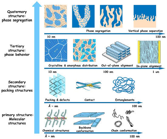
Figure 1.
Various multiscale microstructures of semiconducting polymers that can be generated at different size scales. Reproduced from ref. [99] [Copyright (2023), with permission from the American Chemical Society].
For example, semiconducting polymers owe their electrical conductivity to their unique backbone structure, characterized by alternating single and double bonds between carbon atoms. Both types of bonds feature localized σ components, while the double bonds also include less localized π bonds (Figure 2a) [86]. When monomers link to form long polymer chains, the repeating pattern of alternating σ and π bonds facilitates the delocalization of π orbitals. This delocalization allows π-electrons to move along the conjugated backbone, promoting various electronic interactions that lead to the formation of bonding and antibonding orbitals throughout the polymer chain [86,91].
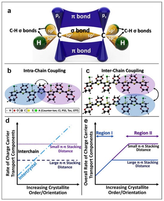
Figure 2.
(a) An example of schematics depicting the σ and π bonds in a semiconducting polymer. Here, each carbon atom displays three σ bonds (two formed with hydrogen and one with the neighboring carbon atom), and one 2pz orbital that forms π bonds, with the latter being orthogonal to the σ plane and eventually delocalized along the polymer chain. (b,c) Schematics showing intra- (a) and interchain (b) coupling in semiconducting polymers. The wave functions of localized charge defects can overlap along a polymer chain, enabling the intrachain coupling. When the distance between individual polymer chains is small, the interchain coupling becomes significant. This interaction enhances the charge transfer integral and increases carrier mobility in conjugated polymers. (d) Schematics emphasizing the rates of intercrystallite and interchain charge transport in (semi)conducting polymers. The blue dashed-dot line represents the rate of intercrystallite charge transport as a function of increasing crystallite order or orientation. Charge transport is more efficient at smaller π–π stacking distances (shown by the dotted purple line) compared to larger π–π stacking distances (depicted by the dashed dark-blue line). (e) Illustration of the overall rate of charge carrier transport combining both intercrystallite and interchain processes. Here, region I represents the low structural order, while region II stands for the high structural order. Increasing the degree of order in region I enhances the electrical conductivity, while the latter is relatively unaffected by the π–π stacking distance. In contrast, in region II the overall charge transport rate plateaus for both small and large π–π stacking distances, indicating that further improvements in order or orientation have a rather limited impact. However, reducing the π–π stacking distance in region II can still significantly improve the overall charge transport rate and electrical conductivity. Reproduced from ref. [86] (a–e) [Copyright (2020) the authors, with permission from Elsevier Ltd.].
It is clear that understanding charge transport in semiconducting polymers is essential for optimizing their material properties and enhancing their performance in various energy devices. A comprehensive understanding of charge transport requires an in-depth knowledge of the transport mechanisms occurring within a single polymer chain, between two or more chains, and at the level of different assemblies of semiconducting chains, such as more or less ordered aggregates and crystallites. Therefore, it is necessary first to understand the interchain and intrachain coupling in semiconducting polymer chains. Intrachain coupling enables charge carriers to move along the polymer backbone through adjacent localized segments. In contrast, interchain coupling facilitates charge hopping between localized sites on different polymer chains or between segments of the same chain that undergo folding (Figure 2b,c) [86]. It is important to emphasize that intrachain coupling is generally stronger than interchain coupling, often resulting in higher charge carrier mobility along the polymer backbone. However, strong interchain coupling plays a crucial role in minimizing charge localization, especially in the presence of structural defects and amorphous regions [86].
Secondly, our goal is to emphasize how aggregates and crystallites, exhibiting a specific degree of molecular order or crystallinity, may impact charge carrier transport. For instance, factors known to enhance intercrystallite charge transport include the degree of order or crystallinity, the size of aggregates or crystallites, their molecular orientation, and the presence of tie chains interconnecting various crystallites [86]. These factors can be controlled by employing the most appropriate processing methodologies, with the primary objective of reducing the π–π stacking distance to generate strong interchain coupling (charge carrier mobility increases as the π–π stacking distance decreases; see Figure 2d) [86]. Conversely, a larger π–π stacking distance typically results in weaker interchain coupling and, consequently, decreased charge carrier mobility. It is important to note that to enhance charge transport, both interchain and intercrystallite charge transport must be optimized through minimization/maximization of the structural disorder/order at the nano- and microscale. While, experimentally, it is possible to reach a limit in crystallite order and orientation (see region II in Figure 2e), additional processing treatments such as doping or the use of additives can often further reduce the π–π stacking distance, thereby improving charge transport even more [86].
We conclude this section with a brief discussion of the most common orientations observed in semicrystalline assemblies (crystallites) typically formed by semiconducting polymers. These orientations include disordered, face-on, edge-on, and end-on orientations (Figure 3a–c) [86,87]. In both face-on and edge-on orientations, the polymeric backbones are aligned parallel to the substrate surface, whereas in the end-on orientation, the backbones are oriented perpendicular to the substrate. This latter orientation is characteristic of highly ordered structures such as single crystals [28]. These orientations are achieved through various processing techniques, including multiple film casting methods and post-fabrication treatments such as thermal and melt-annealing, solvent vapor annealing (SVA), mechanical shearing, rubbing, stretching, hot pressing, and others [100]. Molecular orientation is typically determined using X-ray scattering and diffraction measurements, as the periodic planes of most atomic or molecular species diffract incident X-ray beams of specific wavelengths (noting that the crystalline orientation is indicated by the direction of the diffracted beam) (Figure 3d–h). Key parameters related to molecular interactions and structure can be extracted from X-ray analysis, including the fraction of edge-on and face-on orientations (Figure 3i), the π–π stacking distance (the distance between the centers of aromatic parallel or offset rings) and the crystallographic d-spacing (distance between parallel planes of atoms or molecules within a crystal lattice). Further details on X-ray and other techniques used to determine preferential orientations in semiconducting polymer films can be found in comprehensive reviews available in the literature [86,99].
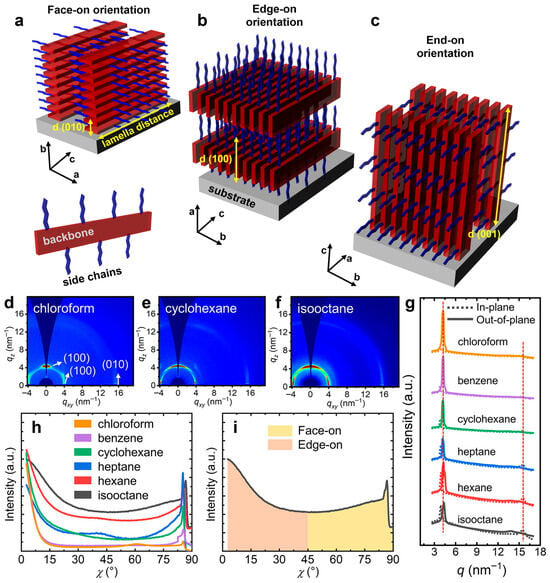
Figure 3.
(a–c) Illustration of different crystallization orientations frequently found in semiconducting polymer thin films: face-on (a), edge-on orientation (b), and end-on (c) orientation. As one can observe, the conjugated backbone is parallel to the surface of substrate in the case of both face-on and edge-on orientations, whereas it is orthogonal with respect to the substrate in the case of end-on orientation. (d–f) 2D GIWAXS patterns of PCDTPT-ODD films drop-cast from solutions of chloroform (d), cyclohexane (e), and isooctane (f). Here, GIWAXS patterns reveal that in PCDTPT-ODD films drop-cast from chloroform solution the content of edge-on orientations is over 74%, whereas this content decreases below 54% in film analogs drop-cast from isooctane solution (similarly, the content of face-on orientations increases from over 25% to more than 46%). (g) 1D GIWAXS plots along the out-of-plane and in-plane directions measured for PCDTPT-ODD films drop-cast from various solutions. (h) Intensity distribution of the (100) peak as relative to the azimuth angle χ for various PCDTPT-ODD films. (i) Fraction of face-on and edge-on orientations extracted for various PCDTPT-ODD films relative to the χ angle. Reproduced from ref. [87] (d–i) [Copyright (2021), with permission from the American Chemical Society].
Finally, it is important to evaluate the efficiency of charge carrier transport in the aforementioned crystalline orientations. It is now well established that charge transport is anisotropic, with charge carrier mobility generally higher along the conjugated backbone (i.e., intrachain) than along the orthogonal direction of the interchain π–π stacking [90,101,102]. Moreover, the actual landscape within thin films of semiconducting materials is often more complex, characterized by a variety of multiscale structures. Therefore, additional factors and structures must be optimized to enhance overall charge transport and charge carrier mobility in these materials. Of particular importance are grain boundaries—interfaces within a polycrystalline film where two or more crystals with different orientations meet—and the abundance of so-called tie chains that interconnect crystalline or ordered domains, creating continuous pathways for charge carrier transport. Fewer grain boundaries and a higher abundance of tie chains both promote increased charge carrier mobilities [28,87]. More detailed information on the effects of molecular conformations and morphology on charge transport processes in semiconducting polymer films can be found in the literature [87,88,89], along with additional theoretical studies that can relate the processing and multiscale structural order of various semiconducting compounds to their optoelectronic properties and device performance [103].
3. Polymeric Semiconducting Nanostructures Displaying High Charge Carrier Mobilities
3.1. Carrier Mobility in Diketopyrrolopyrrole-Based Nanostructures
The enhancement of optoelectronic properties in semiconducting polymers—including charge carrier mobility, electrical conductivity, and photovoltaic performance—is crucial for the development of state-of-the-art nanotechnological applications such as OSCs, OFETs, and OLEDs. We begin by emphasizing the ability of semiconducting polymer chains to transport various charges through hopping between chains or traveling along them. More precisely, we relate charge carrier mobility (µ) to the speed at which charge carriers, such as electrons or holes, can move along or between polymer chains relative to a reference direction in the presence of an electric field [104]. As we will observe, this reference direction is typically preferred either along the π–π stacking axis or along the long chain axis, known as the backbone. Moreover, semiconducting polymeric systems generally exhibit high mobility due to cofacial π-electron system to π-electron system interactions, which are also responsible for photoluminescence quenching [105]. More theoretical details on charge carrier mobility in semiconducting polymers can be found in the literature [106]. Finally, it is worth noting that we will primarily focus on recent scientific reports published roughly within the last five years that discuss charge carrier mobility in semiconducting polymers. Earlier studies (prior to 2020) will be briefly mentioned, as the most significant charge mobilities recorded for various polymers have been comprehensively summarized in several extensive reviews available in the literature [86,107,108,109,110]).
Over the past five years, research on charge mobility in semiconducting polymers has predominantly focused on systems based on DPP. This trend has persisted since the 2013–2015 period, when high charge mobilities of µ = 7 cm2V−1s−1 and µh = 24 cm2V−1s−1 were reported for a PDTTDPP copolymer [111], and a highly crystalline DPPBTSPE system [29], respectively. Both polymers were drop-cast from solutions processed in advance using simple thermal protocols, resulting in highly ordered nanowires. Additionally, a longer DPPBTSPE that produced nanowires with weaker π–π stacking upon processing exhibited a mobility of only 4.15 cm2V−1s−1 [29], underscoring the critical role of molecular packing strength in the π-π direction. Moreover, 24 cm2V−1s−1 remains a record for DPP-based polymers, as subsequent reports of mobilities for over 60 BPP-based polymers did not exceed µh = 17.8 cm2V−1s−1 [108,109,112,113,114,115]. This latter value was achieved for a DPP-selenophene vinylene selenophene (DPP-SVS) polymer containing linear spacer groups, which was solution-sheared and thermally annealed to form well-interconnected granular nanodomains [115].
Relatively high hole mobilities were also observed (see Table 1) in DPP-2T [113], PDPPy-Se [112], or PDPPT3 (see its chemical structure in Figure 4a) [114]. In these cases, polymer chains tended to pack into strong aggregates, large-scale crystallites, or highly continuous structures interconnected by tie chains, respectively. Notably, the presence of tie chains was reported to yield the highest hole mobility measured in a typical OFET device (Figure 4b) for polymer chains with an intermediate molecular weight of Mn = 88 kg/mol (Figure 4c), suggesting the existence of improved transport pathways via tie chains (Figure 4d) [114].
More recently, other DPP-based polymers have been designed and synthesized to fabricate more efficient OFETs. Reports on such polymers have revealed hole mobilities ranging from 2.2 × 10⁻³ to 13.77 cm2V−1s−1 [116,117,118,119,120,121] (see the typical OFET characteristics presented in Figure 4e–g), for films composed of smooth surfaces with nanopinholes [120] or one-dimensional (1D) rod-like nanostructures of tuned molecular weight (Figure 4h) [119]. In contrast, electron mobilities up to 7.76 cm2V−1s−1 were reported for fiber-like domains exhibiting face-on packing and a relatively short π–π stacking distance of 0.370 nm (Figure 4i,j) [118]. Nonetheless, the aforementioned polymers are not particularly suitable for flexible OFETs. Therefore, DPP-based polymers with additional flexible blocks, such as PDPP-TT-PDMS, have been recently designed and optimized [122]. These systems can be processed through solution shearing combined with thermal annealing (TA) to produce highly interconnected fiber-like nanostructures capable of transporting charges with a respectable mobility even when stretched [122]. Other polymers can also be used for fabricating stretchable OFETs, notably P(g2T-T) and P(gT2), both capable of transporting charges at more than 0.35 cm2V−1s−1 through highly aligned crystalline structures interconnected with tie chains and fabricated using TA [123]. Additional information on charge mobilities recently reported for semiconducting polymers based on DPP can be found elsewhere [124].

Figure 4.
(a) Chemical structure of PDPPT3. (b) Schematics depicting a typical OFET device in a top-gate/bottom-contact configuration. (c) Plot depicting the impact of polymer Mn on the hole mobility. (d) AFM height image depicting the microstructure of a thin film of PDPPT3. The inset is a schematic representation of the microstructure of PDPPT3 chains of Mn = 88 kg/mol, with the emphasis on tie-chains. (e,f) Typical electrical measurements evaluating the OFET devices made of TDPP-Se (Mn = 40.7 kg/mol) and recorded in the parallel direction: transfer (e) and output (f) characteristics referring to ID versus VG at a fixed VD, and to ID versus VD at various fixed VG, respectively. (g) Saturation mobility against VG in the parallel direction for devices measured in (e,g). (h) AFM topography micrograph depicting a TDPP-Se film bar-coated from D-ODCB solution onto a substrate kept at 120 °C. (i) AFM height micrograph showing the fiber-like microstructure of a P(TDPP-TQ) film. (j) 2DGIWAXS pattern of P(TDPP-TQ). Reproduced from ref. [114] (a–d) [Copyright (2020), with permission from the American Chemical Society], ref. [119] (e–h) [Copyright (2022) WILEY-VCH Verlag GmbH with permission from John Wiley and Sons], and ref. [118] (i,j) [Copyright (2022) the author(s), with permission from Springer Nature].

3.2. Carrier Mobility in Thiophene-Based Nanostructures
Possibly the second most studied class of semiconducting polymers in terms of charge mobility—and thus widely employed in OFETs—is the class of polythiophene-based systems. The remarkable charge mobility journey of polythiophenes began in 1986, when polythiophene was shown to exhibit mobilities in the range of 10−5 cm2V−1s−1 [125]. This progress has continued to the present day, with maximum mobilities in thiophene-based materials demonstrated to exceed 92 cm2V−1s−1 [96]. Although numerous studies have been reported on common polythiophene systems such as P3OT [126,127] and P3HT [126], the most notable charge mobilities reported in the literature remain the values of 0.62 cm2V−1s−1 [126] and 0.5 cm2V−1s−1 [90], measured in single crystals using OFET and C-AFM configurations, respectively. These values were only surpassed in random polythiophene copolymers, where mobilities of 1.37 cm2V−1s−1 were recorded [128], or in the case of polythiophene isomers, with a reported mobility of 4.6 cm2V−1s−1 [129]. It is important to note that single crystals are highly ordered structures in which all constituent molecules adopt a unique molecular arrangement, with chains often exhibiting a fully extended conformation and end-on orientation [28], which particularly favors intrachain charge mobility. In such molecular assemblies, the side chains may undergo interdigitation, while the backbones interact strongly in the π–π stacking direction leading to small π–π spacings (of only 0.330 nm [28]).
A good mobility of 0.116 cm2V−1s−1 was recently reported in P3HT nanofibers obtained by TA [130]. In this case, a π–π spacing of 0.384 nm was measured. In contrast, nanofibers of P3HT-b-PDL displayed a lower mobility of 0.088 cm2V−1s−1, most likely due to weaker stacking along the π–π direction, as indicated by the slightly larger π–π spacing of 0.385 nm [130]. It is also worth mentioning that a slightly higher mobility of 0.12 cm2V−1s−1 was recently measured in regio-regular P3HT domains that were unidirectionally aligned using a unidirectionally floating-film transfer method [131].
In parallel with P3OT and P3HT systems, numerous other thiophene-based systems have been designed and developed, often incorporating BTBT, DNTT, DBTTT, CDT or IDT. Until 2020, such polymers, often aligned with respect to the substrate, exhibited charge carrier mobilities in the range of 10-20 cm2V−1s−1 [107,132,133]. For example, the alignment of CDT-BTZ polymer chains generated hole mobilities of 11.4 cm2V−1s−1 [132], while PDFDSe highly crystalline chains adopting well-packed edge-on orientations were capable of transporting holes at a maximum mobility of 20.3 cm2V−1s−1 [133]. At the same time, electron mobilities in dithiophene-based polymeric systems were shown to be less than 3.8 cm2V−1s−1 [134]. Intriguingly, CDT-BTZ polymer chains assembled into highly ordered fiber-like single crystals led to a mobility of only 5.5 cm2V−1s−1 along the polymer backbone direction [135].
In the past five years, although the record charge mobility values exhibited by this category of thiophene-based materials have not been surpassed, several notable studies have been reported. Notably, these include the fabrication of continuous nanostructures of a D-A PBDP-F2 [136], generation of fibrillar nanostructures of F8T2 [137]; and the realization of nanostructures composed of large crystallite grains of BDT)-based polymer chains [138]. These were achieved using processing techniques such as simple TA, as well as on-center and off-center spin coating combined with TA; these nanostructures exhibited maximum hole OFET mobilities ranging from 1.93 cm2V−1s−1, to 5.4 cm2V−1s−1, to over 8 cm2V−1s−1, respectively. The highest value was recorded for off-center spin-coated structured films displaying a short π–π spacing of 0.382 nm. In contrast, the counterpart film fabricated via on-center spin coating was less densely packed in the π–π direction (0.386 nm) and generated a hole mobility of only 5.56 cm2V−1s−1 [138], demonstrating that a decrease in π–π spacing typically triggers an increase in charge mobility. In conclusion, all the aforementioned charge mobilities are surpassed by the record-high charge mobility of 92.64 cm2V−1s−1 measured in nanowires of PCDTPT (Mw = 76 kg/mol) fabricated using liquid-bridge-mediated nano-transfer molding [96].
3.3. Carrier Mobility in Naphthalenediimide-Based Nanostructures
NDI-based polymers represent a promising category of semiconducting polymers capable of experiencing high charge mobilities. This subsection begins by revisiting research from approximately ten years ago, when electron mobilities exceeding 1 cm2V−1s−1 were reported for OFETs fabricated from P(NDI2SiC6-T2) [139] and PNDI-RO [140]. Both polymers demonstrated excellent crystallinity and were processed via spin coating followed by TA, resulting in either fibrillar structures with an increased fraction of face-on lamellar orientations [139], or interconnected crystalline grains approximately 120 nm in size with strengthened intermolecular interactions that promote superior charge-transport properties [140].
During approximately the same period, other new NDI-based polymers were reported to display electron mobilities exceeding 5 cm2V−1s−1. For example, the P(NDI2OD-T2) n-type system was pre-aggregated in mesitylene and wire-bar-coated at room temperature to produce shear-aligned nanostructured films with a highly oriented functional surface capable of transporting electrons along the deposition direction at a rate of 6.4 cm2V−1s−1 [141] (note that the same system, but with approximately three times higher molecular weight, was also used to fabricate microwire-like crystals via controlled self-seeding; however, the reported charge carrier mobility only slightly exceeded 2.5 cm2V−1s−1, see ref. [142]). Similar electron mobility values of 6.50 cm2V−1s−1 and 5.64 cm2V−1s−1 were reported for PNDIF-T2 and PNDIF-TVT, respectively [143]. The corresponding thin films, made by spin coating and subjected to TA, consisted of long-range superstructures composed of “backbone” and “side-chain” crystals generated by the strong self-organization of semi-fluoroalkyl segments into highly ordered crystallites [143].
In 2019, Wang and coworkers surpassed the barrier of 7 cm2V−1s−1 for the electron mobility of NDI-based polymers [144]. Specifically, to achieve a highly planar backbone conformation, they incorporated vinylene spacers into an NDI-based polymer, previously synthesized by copolymerizing dibromo-NDI with tin monomers of SNT. Subsequently, they fabricated thin films with enhanced crystallinity and molecular packing, characterized by an exceptionally short π–π stacking distance (0.340 nm) and bimodal distributions of both parallel and perpendicular orientations relative to the π-stacking planes [144]. As a result, a unipolar maximum μe of 7.37 cm2V−1s−1 was demonstrated [144], a value that remains representative for this class of semiconducting polymers today.
More recently, new NDI-based systems have been reported, although their charge mobilities remain relatively average at present. One notable example is the P(NDI2OD-Se-Th 1.0). Synthesized by Lee and coworkers, this polymer was used to fabricate, via TA, surfaces composed of face-on packed crystalline structures that exhibited a modest OFET charge mobility [145].
3.4. Carrier Mobility in Isoindigo-Based Nanostructures
IID-based semiconducting polymers demonstrated significant charge mobility characteristics in 2014, when Kim and coworkers reported a maximum hole mobility of 14.4 cm2V−1s−1 [95] (prior to this, reported charge mobilities were typically in the range of a few cm2V−1s−1, as indicated by refs. [109,110,146]). To achieve this record value, they synthesized a novel D-A polymer named PTIIG-Np and used it to fabricate thin films, which were subsequently exposed to TA to generate highly aligned nanofibrillar networks. These densely ordered lamellar structures, characterized by short π–π stacking distances (0.361 nm) and exhibiting a bimodal distribution of both edge-on and face-on orientations, were responsible for the reported high mobility [95].
Many scientific articles published on IID-based polymers by various research groups between 2015 and 2021 have reported hole mobilities ranging from several to slightly over 8 cm2V−1s−1 [109,110,146,147,148], with a record electron mobility of 9.7 cm2V−1s−1 [149]. The latter was measured in OFET devices incorporating thin films of a highly crystalline polymer (P2FIID-2FBT; based on IID and 3,3′-difluoro-2,2′-bithiophene/2FBT), which, upon TA, formed uniform, large fiber-like polycrystalline grains characterized by effective π–π stacking [149].
More recently, novel IID-based polymers, P(TzII-dTh-dTh) and P(TzII-dTh-dTz), were synthesized by copolymerizing TzII with bithiophene and bithiazole, respectively [150]. Thin films fabricated from these polymers and processed via TA were shown to exhibit poorly crystalline structures. When incorporated into OFET devices, the P(TzII-dTh-dTh) polymer demonstrated the highest hole mobility, while the P(TzII-dTh-dTz) polymer showed the highest electron mobility [150]. However, both values remain modest compared to the other mobility values reported for IID-based polymers discussed above.
3.5. Carrier Mobility in Nanostructures Based on Other Semiconducting Polymeric Systems
Highly ordered structures, such as nanowire single crystals composed of rigid rod-like PPE-based polymers, were shown already in 2009 to display good OFET charge carrier mobilities (0.1 cm2V−1s−1) [31]. A year earlier, several polymers —including PFO and PFO copolymers Y80F8:20F5 and S50F8:50F5, which contained, respectively, 20% and 50% 9,9-di(2-methyl)butyl substituted fluorene units, respectively—were aligned into nematic structures by spin coating from heated solutions. However, the resulting time-of-flight charge mobilities were very modest (µ = 2.7 × 10⁻⁴ cm2V−1s−1) [105].
More recently, Chen and coworkers synthesized new semiconducting PNBDO-FDTE containing varying percentages of additional TFE segments [151]. By spin-casting thin films of these polymers and subjecting them to TA, they generated crystalline structures composed of molecular self-assemblies exhibiting π–π spacings ranging from 0.329 nm to 0.357 nm. Polymers with the highest TFE content demonstrated the highest OFET electron mobilities (µe = 7.43 cm2V−1s−1, respectively) [151].
Other categories of promising semiconducting polymers exhibiting good charge mobilities include F4BDOPV-2T and polymers based on quinacridone (QA). The highest hole mobility in QA-based systems (slightly over 1 cm2V−1s−1) was demonstrated in hydrogen-bonded self-assembled block- and fiber-shaped structures generated by TA [152]. A relatively high charge carrier mobility was also recently reported in ordered structures of F4BDOPV-2T (Figure 5a), fabricated using the self-seeding method (Figure 5b). These structures were shown to be microwire-like crystals (Figure 5c) characterized by high molecular order (Figure 5d,e) [142]. Due to a lower hopping energy barrier present in such microwire-like structures, a charge carrier mobility of 5.58 cm2V−1s−1 was measured along the polymer chain backbone. Nonetheless, the record electron mobility for this class of polymers remains that reported in 2016 by Zheng and coworkers (14.9 cm2V−1s−1) [153], who fabricated thin films of F4BDOPV-2T by combining slow spin coating and TA to generate surfaces composed of large, highly ordered edge-on packed crystallites exhibiting very short π–π stacking distances (0.352 nm) and increased coherence length [153]. A comprehensive comparison between the highest carrier mobilities measured for the aforementioned and other classes of semiconducting polymers can be seen in Figure 5f.
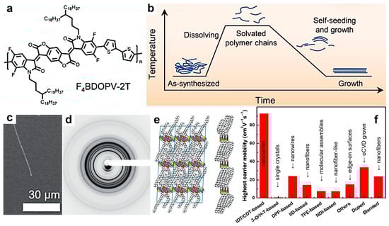
Figure 5.
(a) Chemical structure of F4BDOPV-2T. (b) Diagram depicting the self-seeding method used to grow microwire-like crystals of F4BDOPV-2T. (c,d) Scanning electron micrograph (c) and 2D powder XRD pattern (d) of F4BDOPV-2T crystals grown from polymer seeds initially produced by slowly cooling the solution from 140 °C to 25 °C. (e) Lamellar packing (left) and π–π packing (right) of F4BDOPV-2T molecules within the microwire-like crystals, as inferred from molecular modeling. Here, gray stands for C, white represents H, red is O, blue is N, cyan is F, and yellow is S. (f) Illustration of highest carrier mobilities corresponding to different classes of semiconducting polymers. Reproduced from ref. [142], [Copyright (2021) WILEY-VCH Verlag GmbH with permission from John Wiley and Sons].
3.6. Improved Carrier Mobility in Semiconducting Polymers Blended with Other Polymers
Despite their widespread use in various energy-based applications, semiconducting polymers face significant challenges in future optoelectronic devices, particularly due to their limited environmental stability, poor stretchability, and generally low charge carrier mobility. These limitations are largely influenced by the molecular arrangements of polymer chains at the nano- and microscale. One potential strategy to address these issues is blending semiconducting polymers with insulating and thermoplastic polymers or elastomers. By understanding and controlling processes such as microphase separation in more or less miscible polymer systems, it may be possible to create microstructures that enhance charge transport mechanisms and introduce new material properties, including improved flexibility and stretchability—features that are crucial for the advancement of wearable optoelectronics.
Obviously, one of the most widely used semiconducting polymers in such blends is the P3HT system. Reports in the literature have demonstrated that P3HT can be successfully blended with PDMS, PMMA, PS, PE, HDPE, MEH-PPV, SEBS and others [97]. The most efficient combinations in terms of charge mobility appear to be P3HT/PDMS [154] and P3HT/SEBS [155] blends. The latter exhibit top insulator and bottom semiconductor nanofiber phase-separated morphologies. The P3HT/PDMS microstructure was obtained through solute-solute and solute-surface interactions combined with semiconductor aggregation and exhibited a charge mobility of 0.24 cm2V−1s−1, approximately twice that of analogous neat P3HT films [154]. In contrast, the P3HT/SEBS microstructure was generated through solute-solvent and solute-substrate interactions and demonstrated charge mobilities approaching 0.7 cm2V−1s−1 [155]. However, none of these results match the performance of P3HT nanofibers produced by electrospinning and embedded in a gel composed of PEGDA, HOMPP, and EMIM TFSI, all deposited on stretchable fibers of SBS. This complex system yielded stretchable OFETs capable of charge transport at a record 23 cm2V−1s−1 when unstretched, and 18 cm2V−1s−1 after more than 1500 cycles of stretching at a strain level of ε = 0.7 [156].
Other promising blends (Table 1) include combinations of (i) PDPP-DTT, PDPP3T, PCDTPT, or P(NDI2OD-T2) with PS; (ii) PQT or PDPP-TVT with PMMA; and (iii) PDPP-DTT with SEBS [97]. In these cases, the highest charge mobility of 23.7 cm2V−1s−1 was demonstrated for the PCDTPT/PS microphase-separated morphology, which consists of unidirectional PCDTPT fibrils embedded in the insulating PS matrix. This morphology was obtained through solute–substrate interactions in nanogroove surface relief patterns [157].
More recently, new blend microstructures (Table 1) have been developed, consisting either of semiconducting nanopillars self-assembled under nanoconfinement in a blend of P3HT and PTB7-th [158], or of fibrillar nanostructures and nanoclusters generated by thermally annealing a blend composed of a DPPF-NTz polymer and SEBS [159]. However, the extracted charge carrier mobilities were modest, measuring only 0.73 cm2V−1s−1 and 0.0024 cm2V−1s−1, respectively.
It is also worth mentioning three other interesting blends (Table 1). The first blend consists of P(DPP-T) and BPE [160]. In this case, the microphase-separated granular nanostructures obtained via slot-die coating and direct-ink writing techniques resulted in a hole mobility of only 7 × 10⁻⁴ cm2V−1s−1 [160]. The second blend is formed by mixing a stretchable PU(DPP)35 with PDPPT325% [161]. This blend, upon TA, generated upon TA large microphase-separated domains exhibiting a charge mobility of 1.28 cm2V−1s−1 [161]. The third blend is a mixture of P2TDPP2TFT4 and SEBS [162]. When subjected to a solution shearing method, this blend formed nanofibers displaying charge mobilities up to 2 cm2V−1s−1 [162].
3.7. Enhancing Carrier Mobility of Semiconducting Polymers by Chemical Doping
Unlike inorganic semiconductors, where trace impurities at parts-per-million levels can effectively reduce the band gap, doping semiconducting polymers requires much higher concentrations. Efficient doping of these polymers involves adding strong oxidizing agents for p-type doping or strong reducing agents for n-type doping. This process often affects a substantial portion of the monomer units—typically between one-third and two-thirds—corresponding to doping concentrations of approximately 1019 to 1021 cm−3 [86]. Although chemical or electrochemical doping is primarily used to enhance the electrical performance of semiconducting polymers by either removing an electron from the HOMO through oxidation or adding an electron to the LUMO through reduction, it also has significant consequences on the corresponding charge mobilities.
For example, the pristine PEDOT system, which typically exhibits charge mobilities on the order of 10−4 cm2V−1s−1 [163], has been shown to achieve Hall charge mobilities as high as 33.6 23 cm2V−1s−1 in doped PEDOT thin films fabricated from the EDOT monomer and FeCl3 oxidant using the oCVD method [164]. PEDOT is often combined with PSS in the well-known PEDOT:PSS composite, which exhibits excellent electrical conductivity and is used in various high-tech applications. More information on the charge mobility of PEDOT, PEDOT:PSS and various PEDOT:PSS composites can be found in recent comprehensive reviews published in the literature [86,165].
Another example illustrating the impact of doping on charge mobility is P3HT. As previously noted, the highest charge mobility in P3HT (0.5 cm2V−1s−1) was reported for highly ordered single crystals composed of fully aligned and interdigitated chains [90]. By chemically doping P3HT, this mobility limit can be increased to 0.8 cm2V−1s−1, as demonstrated by Stanfield and coworkers, who doped P3HT with F4TCNQ and optimized the casting solvent for the dopant [166]. P3HT can also be doped with other dopants such as DDB [167] and CPE [168], but the extracted charge mobilities are relatively modest.
In conclusion, the highest charge mobility recorded so far for a semiconducting polymer is 92.64 cm2V−1s−1 measured for nanowires of PCDTPT (Table 1). This value aligns with theoretical studies suggesting that the mobility limit for polymeric systems could reach 100 cm2V−1s−1 [107]. However, we do not discuss in this work the ladder-type 2DCPs which have demonstrated charge mobilities as high as 970 cm2V−1s−1, as recently shown for the 2DCP-MPc ladder-type polymer [169].
Finally, it is worth noting that most of the aforementioned processing methods, which produce various highly ordered nanostructures characterized by optimal molecular packing and high carrier mobilities, rely on widely employed film deposition techniques such as solution shearing, bar coating, spin coating, drop casting, and thermal treatments like TA. Techniques such as solution shearing and bar coating offer greater control and are therefore more efficient in producing densely packed nanostructures, while also demonstrating promising potential for scalability. Consequently, these techniques could be employed in large-scale applications. In contrast, spin coating, drop casting, and similar methods tend to produce nanostructures with less efficient packing at the micro- and nanoscale, especially without TA, and exhibit limited scalability due to the restricted size of the polymer films produced. As a result, these methods are more prone to failure or remain limited in practical device applications.

Table 1.
Summary of the most recent charge mobilities reported in the literature for various semiconducting polymers. Most relevant results are marked in gray.
Table 1.
Summary of the most recent charge mobilities reported in the literature for various semiconducting polymers. Most relevant results are marked in gray.
| Polymer System (* = Full Name) | Molecular Weight (kg/mol) | Nanostructure Type | Processing Strategy | π–π Spacing (nm) | Measurement Technique | Charge Mobility (cm2V−1s−1) | Current On/Off Ratio | Threshold Voltage (V) | Ref. |
|---|---|---|---|---|---|---|---|---|---|
| DPP-based polymers | |||||||||
| PDTTDPP | - | nanowires | thermal protocols and drop casting | 0.370 | OFET | µ = 7 | - | −15 | [111] |
| DPPBTSPE | Mn = 8 | nanowires | thermal protocols and drop casting | 0.346 | OFET | µh = 24 | 104 | −4 | [29] |
| DPPBTSPE | Mn = 68 | nanowires | thermal protocols and drop casting | 0.372 | OFET | µ = 4.15 | 108 | 0 | [29] |
| DPP-2T | Mn = 74 | strongly packed aggregates | TA | 0.380 | OFET | µh = 1.33 | 104 | −3 | [113] |
| PDPPT3 | Mn = 88 | high continuity structures with tie chains | TA | 0.372 | OFET | µh = 4.9 | 104–105 | −7 to −15 | [114] |
| PDPPy-Se | Mn = 409.1 | large-scale crystallites | TA | 0.362 | OFET | µe = 2.22 | - | − | [112] |
| P(gDPP-TT) P(gDPP-T2) P(gDPP-MeOT2) | - - - | (highly) ordered and crystalline edge-on oriented surfaces | spin coating | 0.358 0.354 0.352 | OECT | µ = 0.57 µ = 1.55 µ = 0.28 | 105 105 104 | −0.54 −0.52 −0.26 | [117] |
| P(TDPP-BT) P(TDPP-TQ) P(TDPP-BBT) | Mn = 42 Mn = 16.1 Mn = 21 | fiber-like domains with face-on packing | TA | 0.357 0.369 0.369 | OFET | µe/h = 3.83/2.77 µe/h = 7.76/6.16 µe/h = 0.35/0.25 | - - - | − − − | [118] |
| TDPP-Se | Mn = 21.2 Mn = 40.7 Mn = 61.3 Mn = 73.3 Mn = 135.3 | 1D rod-like nanostructures | bar-coating | 0.369 0.370 0.370 0.369 0.370 | OFET | µh = 6.47 µh = 13.77 µh = 12.05 µh = 6.81 µh = 7.42 | 103 ÷106 105 ÷107 105 ÷107 104 ÷107 105 ÷107 | −11 ÷ −6 −8 ÷ −3 −7 ÷ 0 −10 ÷ −2 −12 ÷ −6 | [119] |
| NH-FDPP-TT NH-FDPP-BT | Mw = 8.69 Mw = 5.61 | smooth surfaces with nanopinholes | TA | 0.390 - | OFET | µh = 5 × 10⁻³ µh = 2.2 × 10⁻³ | 105 105 | −17.5 −25.4 | [120] |
| PTNDP-IDT PNDP-2T | Mw = 41.8 Mw = 29.2 | coplanar π–π stacked structures | TA | 0.386 0.366 | OFET | µe = 0.99 µe = 0.82 | 6 6 | 17−21 15−18 | [121] |
| IDTz-DPP-based | Mn = 48.5 | amorphous structures without long-range order | TA | - | OFET | µe = 1.3 | - | 2.6 | [116] |
| PDPP-TT PDPP-TT-PDMS-1k PDPP-TT-PDMS-2.5k PDPP-TT-PDMS-25k | Mn = 17.7 Mn = 14 Mn = 14.6 Mn = 37.5 | interconnected fiber-like nanostructures | solution shearing and TA | 0.369 0.363 0.370 0.365 | OFET | µ = 0.7 µ = 0.21 µ = 0.15 µ = 0.1 | ~105 ~106 ~106 ~106 | 22.69 ± 8 29.06± 4 25.76 ± 2 17.08 ± 1 | [122] |
| P(g2T-T) P(gT2) | Mn = 67.5 Mn = 71 | aligned crystalline structures with tie-chains | TA | 0.356 0.374 | OECT | µ = 0.93 µ = 0.38 | - - | - - | [123] |
| 3-octyl and 3-hexyl-thiophene (3-O/H-T)-based polymers | |||||||||
| P3OT | Mw = 120 | single crystal | - | - | OFET | µ = 1.54 × 10⁻⁴ | 37 | 7.3 | [127] |
| P3OT | Mw = 51.2 | single crystal | - | - | OFET | µ = 0.62 | - | - | [126] |
| P3HT | Mw = 39.6 | single crystal | - | - | OFET | µ = 1.57 × 10⁻³ | - | - | [126] |
| P3HT | Mn = 1.332 | single crystal | - | - | C-AFM | µ = 0.5 | - | 8 | [90] |
| P3HT P3HT-b-PDL | Mn = 15 Mn = 29.6 | nanofibers | TA | 0.384 0.385 | OFET | µ = 0.116 µ = 0.088 | 3.9 × 10⁵ 4.5 × 10⁵ | −2.6 −2.6 | [130] |
| RR-P3HT | - | unidirectionally aligned domains | unidirectional floating-film transfer method | - | OFET | µ = 0.12 | 104 | - | [131] |
| Bithiophene, IDT, CDT-based polymers | |||||||||
| CDT-BTZ | Mn = 50 | nanofibers | - | - | OFET | µ = 5.5 | 106 | −60 | [135] |
| s-BTI2-FT f-BTI2-FT | Mn = 19.5 Mn = 13.8 | crystalline edge-on aggregates | TA | 0.360 0.360 | OFET | µe = 0.82 µe = 1.13 | 106 106 | 19 18 | [170] |
| f-BTI2TEG-T f-BTI2TEG-FT | Mn = 6.7 Mn = 6.3 | fibrillar nanostructure | TA | 0.353 0.353 | OECT | µe = 0.044 µe = 0.034 | - | 0.68 0.53 | [171] |
| OFET | µe = 6.34 × 10⁻⁴ µe = 3.67 × 10⁻⁴ | 16.8 1.3 × 10³ | - - | ||||||
| P(g2T-TT) PgBTTT | Mn = 7 Mn = 10 | 2D islands of elongated parallel backbones | drop-casting and electrospray deposition | 0.358 0.354 | OECT | µh = 0.41 µh = 3.44 | - - | - - | [172] |
| PBDP-F2 | Mn = 40.9 | continuous donor and acceptor nanostructures | TA | 0.369 | OFET | µh = 1.93 | - | - | [136] |
| F8T2 | - | fibrillar structures | TA | - | OFET | µh = 5.40 | >105 | -3 | [137] |
| BDT-based | Mn = 12.8 | nanostructures comprising large crystallite grains | on-center vs. off-center and TA | 0.386 0.382 - - | PMMA-gated PMMA-gated pristine OFET functionalized | µh = 0.44 × 10⁻² µh = 1.90 × 10⁻² µh = 5.56 µh = 8.03 | >102 >102 >105 ~106 | −16.90 −26.64 −1.25 −1.47 | [138] |
| C16-IDT-BT | Mw = 108 | - | TA | 0.410 | OFET | µh = 1.2 | - | − | [173] |
| IDT-BT TTIF-BT | Mn = 58 Mn = 51 | surfaces of enhanced crystalline order | TA | 0.410 0.414 | OFET | µh = 1.5 µh = 1.1 | - 106 | 0 −12 | [174] |
| PCDTPT | Mw = 76 | nanowires | liquid-bridge-mediated nano- transfer molding | 0.442 | OFET | µ = 92.64 | 1.8 × 10⁴ | 1.77 | [96] |
| IID-based polymers | |||||||||
| Polyisoindigo Poly(ethynylisoindigo) Poly(bisisoindigo) | Mn = 21.9 Mn = 15.4 Mn = 15.5 | surfaces with different molecular order | TA | 0.370 0.350 0.380 | OFET | µe = 2.85 × 10⁻⁴ µe = 4.15 × 10⁻⁴ µe = 7.67 × 10⁻⁵ | 104 104 104 | 59 57 51 | [175] |
| P(TzII-dTh-dTh) P(TzII-dTh-dTz) | Mn = 236 Mn = 138 | poorly crystalline structures | TA | - - | OFET | µh/e = 1.43/0.55 µh/e = 0.38/0.56 | 103 ~3 | 15.96 79.78 | [150] |
| P2FIID-2FBT | Mn = 59 | fiber-like poly-crystalline grains | TA | 0.350 | OFET | µe = 9.7 | 103–104 | 57 | [149] |
| PTIIG-Np | Mn = 21 | nanofibers | TA | 0.361 | OFET | µh = 14.4 | - | −45÷ −48 | [95] |
| NDI-based polymers | |||||||||
| P(NDI2OD-Se-Th 1.0) | Mn = 70 | surfaces comprising face-on packed crystalline structures | TA | - | OFET SCLC | µ = 0.138 µe = 2.5 × 10⁻⁴ | >103 - | 1.3 - | [145] |
| P(NDI2OD-T2) | Mn = 76.6 | microwire | OFET | µ = 2.56 | - | - | [142] | ||
| SNTandNDI-based | Mw = 54.9 | nanofiber-like crystalline structures | TA | 0.340 | OFET | μe = 7.37 | 106–107 | 1-5 | [144] |
| TFE-based polymers | |||||||||
| PNBDO-FDTE100 PNBDO-FDTE90 PNBDO-FDTE80 PNBDO-FDTE70 PNBDO-FDTE60 PNBDO-FDTE0 | Mw = 164.4 Mw = 117.6 Mw = 115.5 Mw = 108.1 Mw = 105.5 Mw = 76.9 | crystalline structures comprising molecular self-assemblies | spin coating and TA | 0.350 0.350 0.353 0.356 0.357 0.329 | OFET | µe = 7.43 µe = 7.25 µe = 6 µe = 1.75 µe = 062 µe = 0.182 | 102–103 102–103 102–103 ~102 ~102 102–103 | 19.18 18.76 17.5 18.4 14.75 17.73 | [151] |
| Other types of polymers | |||||||||
| PFO Y80F8:20F5 S50F8:50F5 | - | aligned nematic structures | spin coated from heated solutions | - | time-of-flight | µ = 2.7 × 10⁻⁴ µ = 3.7 × 10⁻² µ = 2.7 × 10⁻² | - | - | [105] |
| TA-PPE | Mw = 51.328 | nanowire | OFET | µ = 0.1 | - | −40 | [31] | ||
| F4BDOPV-2T | Mn = 60.4 | microwire | OFET | µ = 5.58 | 103-104 | 2 | [142] | ||
| F4BDOPV-2T | Mn = 38 | surfaces of edge-on packed crystallites | TA | 0.352 | OFET | µe = 14.9 | 103-104 | −17 | [153] |
| QA based | Mw = 38.5 | block- and fiber-shaped structures | TA | 0.356 | OFET | µh = 1.02 | 5-6 | −17 | [152] |
| Doped polymers | |||||||||
| P3HT/CPE | Mw = 80 | ordered crystallites | dopant induced | - | OFET | µh = 0.135 | ~103 | −22.4 ± 2.1 | [168] |
| P3HT/DDB | Mn = 50–70 | lamellar crystallites | spin coating | - | AC-Hall effect | µ = 0.095 | - | - | [167] |
| PEDOT/FeCl3 | - | - | oCVD | - | AC-Hall effect | µ = 33.6 | - | - | [164] |
| Blended polymers | |||||||||
| PCDTPT/PS | Mw = 50 | nanofibers | slow-drying | - | OFET | µh = 23.7 | - | - | [157] |
| P3HT PTB7-th P3HT/PTB7-th | - - - | nanopillars nanopillars nanopillars | self-assembly under nano confinement | 0.373 0.391 0.378:0.387 | conductive scanning force microscopy | µvertical = 0.96 µvertical = 0.036 µvertical = 0.73 | - - - | - - - | [158] |
| P2TDPP2TFT4/SEBS | Mn = 97 | nanofibers | solution shearing | 0.366 | OFET | µ = 2 | 104–105 | - | [162] |
| PU(DPP)35 PU(DPP)35/PDPPT325% | Mn = 20 - | tens to hundred nm large phase- separated domains | TA | - 0.364 | OFET | µh = 0.19 µh = 1.28 | - - | - - | [161] |
| P(DPP-T)/BPE | Mw = 146.3 | phase-separated granular nanostructures | slot-die coating | - | OFET | µh = 1.37 × 10⁻² | 102 | 14.6 | [160] |
| direct-ink writing | - | µh = 7 × 10⁻⁴ | 101 | −13.3 | |||||
| DPPF-NTz/SEBS | Mn = 34 | fibrillar nanostructures and nanoclusters | TA | 0.390 | OFET | µe = 0.0024 | 105 | 4.61 | [159] |
| P3HT/PEGDA/HOMPP based | MwP3HT = 87 | nanofibers | electrospinning | - | OFET | µ = 23 | 105 | −3÷ −2.7 | [156] |
At the end of this section, one must emphasize that chemical doping and polymer blending are widely employed strategies to tailor the optoelectronic properties of semiconducting polymers. However, over the long term, these approaches often introduce significant challenges related to the stability and reproducibility of polymer film properties. These challenges include: (i) chemical instability of dopants (or other blend components), where dopant molecules can diffuse out of the polymer matrix, undergo chemical transformations, or degrade under environmental conditions such as humidity or light exposure, leading to a time-dependent loss of doping efficiency; (ii) morphological instability caused by poor miscibility between various components (e.g., polymer–additive, polymer–fullerene, polymer–polymer, polymer–dopant), resulting in phase segregation through crystallization or aggregation—dopants, small acceptor molecules, or additives can crystallize or aggregate into new morphological structures that disrupt carrier transport pathways; (iii) non-uniform doping and dedoping effects, where even in rare cases when homogeneous doping at the nanoscale is achieved, it does not persist due to slow desorption of dopants, which decreases the free carrier concentration; (iv) reproducibility challenges related to variations in polymer synthesis, dopant or additive purity, inconsistent processing conditions (for example, caused by minor changes in solvent or substrate temperature, humidity variations, etc.), or kinetic trapping of blended or doped films in often unreproducible metastable states; (v) optoelectronic trade-offs caused by photoluminescence quenching and broadening or shifting of absorption and emission spectra; and (vi) degradation of device interfaces, typically induced by the migration of dopant ions or additive molecules to various interfaces, which compromises interfacial stability and, consequently, device performance.
4. The Enhancement of Electrical Conductivity in Nanostructures of Semiconducting Polymers
Electrical conductivity measures a material’s capability to permit the flow of electric current, indicating how easily charge carriers can move through the material when an electric field is applied. The bulk conductivity of a semiconducting polymer is typically determined by charge transport both along individual polymer chains and between adjacent chains. It depends on the type of charge carriers, their mobility and density [40]. While the latter can be effectively tuned by chemical doping—as discussed in this subsection, doping is a widely used method to enhance electrical conductivity in semiconducting polymers, potentially increasing it from insulating to metallic levels (i.e., from 10−10–10−5 S/cm to 104 S/cm [176])—the charge transfer process plays a crucial role in enhancing conductivity at the micro- and nanoscale. This process typically occurs from one crystallite to another and across tie chains connecting crystallites [86]. Therefore, highly ordered nanostructures exhibiting strong interchain packing (i.e., decreased π–π stacking distance) generally promote charge delocalization along and across polymer chains through mechanisms such as hopping and intrachain coupling. Additional factors influencing electrical conductivity in semiconducting polymers are comprehensively reviewed in a recent publication by Pooja and coworkers [177].
There are many semiconducting polymers that exhibit good electrical conductivity, with the most common being PEDOT, PANI, PPy, P3HT, PA, and several others (Table 2). Among these, PEDOT stands out as the most prominent, in terms of electrical conductivity and practical applications. When polymerized via a chemical oxidative method in an aqueous solvent using Fe2(SO4)3 as the oxidant, PEDOT shows a conductivity in the range of 0.0002–0.001 S/cm [178]. This conductivity can be significantly increased to 130 S/cm by assembling PEDOT molecules into high aspect-ratio nanofibers through evaporative vapor-phase polymerization inside a CVD chamber, followed by TA [179]. PEDOT’s conductivity can be further enhanced by employing a novel synthetic strategy that induces surfactant-free interfacial polymerization at the interface of PEDOT and flexible cellulose paper. The resulting PEDOT paper, composed of densely packed π-conjugated chains, exhibits a conductivity of approximately 375 S/cm [180]. Moreover, Massonnet and coworkers synthesized PEDOT-based polymers displaying metallic-like behavior, by using Fe(OTf)3 as the oxidant, achieving a conductivity of 1218 S/cm for PEDOT:OTf [181]. Subsequent treatment of the PEDOT-based polymer in TsOH, TfOH and H2SO4 further enhanced its electrical conductivity to 1503 S/cm, 1613 S/cm, and 2273 S/cm, respectively [181]. These high conductivity values for PEDOT were surpassed by molecularly engineering the crystallization and morphology of PEDOT using oCVD, followed by treatment with hydrobromic acid and precise control of film thickness [182]. The resulting films, composed of highly crystalline, face-on oriented PEDOT chains, exhibited a record-high conductivity of 6259 S/cm [182].
For many technological applications, it is useful to blend PEDOT with PSS to generate PEDOT:PSS water-soluble hole transport layers. Due to the non-conductive nature of PSS, the PEDOT:PSS system exhibits a relatively low conductivity of around 0.02 S/cm [183], but it can typically reach values between 0.25 S/cm [184] and approximately 1 S/cm [181]). Guo and coworkers demonstrated that PSS can be replaced by poly(diphenylamine-4-sulfonic acid) (PDAS) to create a novel water-soluble hole transport layer with significantly higher conductivity (0.135 S/cm) [183]. Fortunately, many formulations of PEDOT:PSS that can be further enhanced with various additives to improve conductivity [185]. Until 2015, the best formulation appeared to be the commercial PEDOT:PSS known as Clevios P, to which DMSO was added. This treatment increased the electrical conductivity from 0.2 to 1 S/cm to 677 S/cm (many other relevant formulations are documented elsewhere [185]). By 2019, these formulations had been further optimized, achieving conductivities ranging from a few thousand to several thousand S/cm [186]. Two of the highest conductivities were obtained for PEDOT:PSS commercially known as PH1000, either by depositing it as a transparent conductor film using the solution shearing approach [187] or by mixing it with additives followed by light oxygen plasma treatment [188]. Consequently, a conductivity of 4600 S/cm was measured in the former case [187], while a record-high value of 5012 S/cm was recorded in the latter [188].
More recently, Chen and coworkers employed a triple-network strategy (Figure 6a) by incorporating a covalently crosslinked network of PEGDA into a PEDOT:PSS hydrogel doped with DMSO. The resulting three-dimensional (3D) porous system was then soaked in acetic acid and rinsed with water. This process was followed by the diffusion of additional PEG chains into the porous structure, yielding a stretchable triple-network hydrogel (TN-H) composed of phase-separated PEDOT and PSS domains (Figure 6b) and pores containing interconnected fibers (Figure 6c). The TN-H system exhibited an overall electrical conductivity of 0.3 S/cm at a stretchability of 900%, a benchmark value to date for all stretchable PEDOT:PSS-based gels [189].
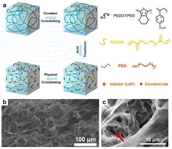
Figure 6.
(a) Diagram depicting the triple-network strategy used to prepare the TN–H hydrogel. (b) A cross-sectional scanning electron microscopy (SEM) image depicting the TN–H gel. (c) A SEM micrograph of the TN-H freeze-dried hydrogel emphasizing the interconnected fibers in its pores (red arrow). Reproduced from ref. [189], [Copyright (2023) the authors, SmartMat published by Tianjin University and John Wiley and Sons Australia, Ltd., with permission from John Wiley and Sons].
Another class of polymers displaying highly effective conductive properties includes PPy and DPP-based systems. Electrical conductivity ranges from 10−6 S/cm for neat DPP-based films [190,191], to 12 S/cm for PPy hydrogels [192], and up to 70 S/cm for DPP-based polymers doped withCN6-CP [190]. Doping DPP-based polymers with FeCl3 has been shown to further increase conductivity from the range of 19–119 S/cm [191,193] to a staggering 997 S/cm [194]. In contrast, the use of N-DMBI dopant typically results in more modest conductivities, ranging from 0.0001 to 8.4 S/cm [124].
Recently, novel DPP-based polymers have been reported in the literature, including PDPIN [195], PTz-5-DPP [196], P(DPP-CNPz) [197], as well as P(DPP-DCNPz) [197]. The PTz-5-DPP, P(DPP-CNPz), and P(DPP-DCNPz) systems doped with N-DMBI delivered conductivities of 8.31 S/cm, 25.3 S/cm, and 33.93 S/cm, respectively. In contrast, the PDPIN system doped with PSpF demonstrated a higher conductivity of 78.1 S/cm. This promising value has been challenging to surpass, even in more recent DPP-based polymers doped with N-DMBI, such as the ThDPP-CNBTz system (56.5 S/cm) [198]; the DPP-BFDO-Th system, based on a quinoidal BFDO unit (65.68 S/cm) [199]; and the PDFSe system, based on an acceptor-triad moiety of DFSe (62.6 S/cm) [200]. The only higher conductivity values—218 S/cm and up to 170 S/cm —were recorded for P(PzDPP-2FT) (Figure 7a) doped with TDAE or CoCp2 (Figure 7b) and further docked with pyridine and imidazole aromatic cations (Figure 7c), respectively [201]. Other significant conductivities in the range of 50–100 S/cm were also measured for P(PzDPP-2FT) docked with various alkyl cations (Figure 7d). These high electrical conductivities were attributed to decreased energetic disorder in the P(PzDPP-2FT)-based system, resulting from docking the cations near the polymer backbone (Figure 7e) [201]. A similar conductivity of 173 S/cm was reported for n-doped P(PzDPP-2FT) fibers (Figure 7f) fabricated using a flow-enhanced crystallization method based on shear flow-induced disaggregation and alignment. These fibers comprised highly planar backbones and crystallized alkyl side chains, which promoted strong interchain π–π stacking interactions (Figure 7g,h) that enhanced electrical conductivity [98]. Additional conductivity data for other polymers doped with various chemicals can be found elsewhere [177].
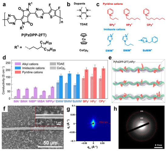
Figure 7.
(a–c) Schematics depicting the P(PzDPP-2FT) (a), TDAE) and CoCp2 dopants (b) and pyridine and imidazole aromatic cations (c). (d) Plot juxtaposing the electrical conductivities recorded for doped P(PzDPP-2FT) films that were docked with various cations. (e) A molecular dynamic simulation emphasizing the docking of P(PzDPP-2FT) with HPy+ cations. (f–h) SEM image (f), 2D small-angle x-ray scattering (SAXS) pattern (g) and selected area electron diffraction (SAED) of a P(PzDPP-2FT) fiber. Reproduced from ref. [201] (a–e) [Copyright (2024) The author(s), with permission from Springer Nature] and ref. [98] (f–h) [Copyright (2024) the authors, some rights reserved; exclusive licensee American Association for the Advancement of Science].
Neat films of P3HT, as well as other thiophene-based systems—including PBTTT derivatives—typically display low electrical conductivities in the range of 10−6 S/cm [202,203]. Upon optimal doping with F4TCNQ, the conductivity of these polymeric systems increases dramatically to 1-2 S/cm [202,203,204], with more recent reports demonstrating conductivities reaching up to 5.6 S/cm [166]. Interestingly, doping aligned films of P3HT and PBTTT derivatives with FeCl3 has yielded exceptional conductivities of 570 S/cm and 2.2 × 10⁵ S/cm, respectively [205]. Additional conductivity values ranging from 3 × 10⁻⁴ to 251 S/cm have been reported for P3HT (including both regioregular and regiorandom forms) doped with various other molecules. These findings are comprehensively summarized in a recent dedicated study [206]. Similarly, notable combinations of PBTTT with various dopants, exhibiting conductivities in the range of 36-1300 S/cm, are documented elsewhere [99].
Other recently developed thiophene-based systems reported to display promising electrical conductivity include polymers such as n-PT4, [207]PO12, [208], PCNI2-BTI polymer [209], and f-BSeI2TEG-FT [210]. For example, the PO12 system (schematically depicted in Figure 8a) doped with N-DMBI, was shown to generate films composed of large, highly crystalline domains intercalated with small dopant domains (Figure 8b) and delivered a conductivity of 92 S/cm at a dopant concentration of 4 mg/mL (Figure 8c) [208]. Notably, analogous systems based on longer or shorter side chains exhibited significantly lower conductivities. Higher conductivities of 103.5 S/cm [210] and 133.3 S/cm [207] were achieved for the f-BSeI2TEG-FT and n-PT4 systems, respectively, when doped with N-DMBI. In the latter case, due to the extremely short side chains of n-PT4 (Figure 8d), doping induced a crystalline fibril-textured morphology (Figure 8e) with improved molecular order, characterized by a short π–π stacking distance of only 0.350 nm (compared to 0.360 nm before doping; see Figure 8f) [207]. Moreover, this efficient π–π stacking of highly doped n-PT4 chains was accompanied by an increased coherence length in n-PT4 films and decreased paracrystalline disorder (Figure 8f). These observations demonstrate that high doping efficiency can be achieved without introducing additional structural disorder into the film microstructure, thereby greatly favoring the increase in conductivity.
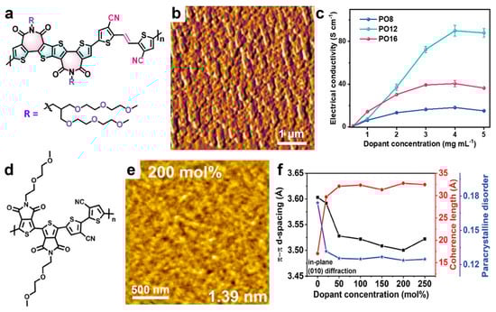
Figure 8.
(a) Chemical structure of PO12 system. (b) AFM phase image depicting the morphology of a PO12 film n-doped with N-DMBI. (c) Electrical conductivities measured against the dopant concentration for PO12 and its analogs displaying longer and shorter side chains, respectively. (d) Chemical structure of n-PT4. (e) AFM topography image depicting the morphology of a doped n-PT4 films using a dopant concentration of 200 mol%. The rms surface roughness is shown in the bottom-right corner. (f) The dependance of π-π stacking distance, coherence length, and paracrystalline disorder on the doping concentration in n-PT4 films. Reproduced from ref. [208] (a–c) [Copyright (2023) the authors. Advanced Science published by Wiley-VCH GmbH, with permission from John Wiley and Sons], and ref. [207] (d–f) [Copyright (2023) Wiley-VCH GmbH, with permission from John Wiley and Sons].
A higher conductivity of 150.2 S/cm was measured for thin films of PCNI2-BTI doped with N-DMBI [209]. These films were prepared via solution shearing, as spin coating proved less efficient, and consisted of highly oriented, fiber-like aggregates showing a preferential face-on orientation. It is worth noting that other imide-based polymeric systems, such as the PDTzSI-Se have demonstrated a conductivity of 164 S/cm when doped with N-DMBI [211]. analogs with lower selenophene content, doped similarly, demonstrated conductivities in the range of 62–98 S/cm.
Other notable polymeric systems exhibiting high electrical conductivity include those based on PPV. Among these are the FBDPPV and FBDPPV-OEG systems [212,213]. When doped with a TAM derivative, thin films of FBDPPV demonstrated conductivities up to 21 S/cm [213]. This value increased slightly to 22.5 S/cm by using shorter FBDPPV chains [212]. In contrast, the FBDPPV-OEG/TAM doped system, initially dissolved in hexafluoroisopropanol, formed disconnected porous regions that facilitated dopant penetration, resulting in a higher conductivity of 39 S/cm [214]. A comparable conductivity (38.3 S/cm) was also observed in films of the PFClTVT system, doped with N-DMBI and composed of nanofiber-like aggregates [215].
Another system worth mentioning in this section is oligoaniline TANI, which can be processed from solutions to generate plate-like single crystals vertically aligned with respect to the graphene guiding substrate. These crystals were shown, using C-AFM, to possess an electrical conductivity of 12.3 S/cm along the π-stacking direction [216]. This value exceeds by more than an order of magnitude the highest conductivity previously reported for TANI in wire-, ribbon-, or plate-like structures produced using a solvent exchange method [217]. It also surpasses the typical conductivity values of 0.1 to 1 S/cm recorded for PANI [176,218], although PANI is capable of reaching conductivities up to 200 S/cm [219]. Moreover, even higher conductivity values of 320 S/cm have been obtained for PANI when self-assembled into tubes with a diameter of 140 nm and doped with TSA [220]. Additional relevant conductivity values for doped PANI can be found elsewhere [177].
Furthermore, polymers based on NDI and doped with N-DMBI have been shown to exhibit moderate electrical conductivities, ranging from 0.008 S/cm for P(NDI2OD-T2) (or N2200) to 1.8 s/cm for the PNDI2TEG-2Tz system [124]. Additional polymer/dopant configurations and their corresponding conductivities can be found in comprehensive recent reviews [99,221,222].
Other polymeric systems exhibiting promising electrical conductivities include biodegradable materials based on PANI, PEDOT, or PPy. Detailed information on the generated nanostructures and their corresponding electrical conductivities can be found elsewhere [223]. Additionally, it is worth mentioning the report by Matsuhisa and coworkers, who prepared an elastic conductor ink by mixing Ag flakes with an elastomeric fluorine copolymer and a water-based fluorine surfactant in an organic solvent [224]. This process resulted in a phase-separated morphology consisting of an elastic core covered by an Ag-dense surface layer, which exhibited an initial conductivity of 738 S/cm. This value decreased to a still high conductivity of 182 S/cm when the elastic conductor was stretched to 215% strain [224]. In this work, we have again excluded ladder-type polymers, which can achieve conductivities in the range of few thousand S/cm. An example of such a system is PBFDO, which can exhibit conductivities exceeding 2000 S/cm in films composed of molecules adopting a preferential edge-on orientation [225].
Finally, it is worth noting that two primary trade-offs remain unresolved or only partially addressed in organic optoelectronics. The first trade-off involves balancing charge carrier mobility with the thermal and morphological stability of thin films composed of semiconducting polymers. This challenge arises from conflicting structural and chemical requirements: achieving high mobility demands high crystallinity and well-ordered, efficiently π–π-stacked nanostructures, whereas such crystalline nanostructures are thermodynamically less stable due to phase segregation caused by possible reorientation, coarsening, or further growth. Therefore, a critical challenge is to identify optimal solutions that maintain high crystallinity for morphological stability without significantly compromising device performance. This entails designing polymers that form nanostructures with a high degree of local order while suppressing macroscopic phase changes through crosslinking or non-covalent interactions. The second trade-off concerns the balance between flexibility/stretchability and electrical conductivity in thin films of semiconducting polymers, which is crucial for advancing flexible optoelectronics, wearable devices, and organic circuits. Electrical conductivity requires long conjugation lengths in planar, rigid backbones, whereas increased flexibility demands deformable backbones composed of soft, potentially elastomeric segments. Moreover, although high crystallinity and doping improve π–π stacking and charge transport, highly crystalline and doped structures are prone to cracking under mechanical strain. Potential solutions include developing semiconducting block copolymers that incorporate elastomeric blocks to combine conductive and stretchable domains; semiconducting polymer-based composites that maintain good conductivity while remaining highly flexible; or ductile crystalline polymers that preserve order under mechanical strain.
Table 2.
Summary of conductivity values recently reported in the literature for various semiconducting polymers. Most relevant values are marked in gray.
Table 2.
Summary of conductivity values recently reported in the literature for various semiconducting polymers. Most relevant values are marked in gray.
| Polymer System/Dopant (If the Case) | Molecular Weight (kg/mol) | Nanostructure Type | Processing Strategy | Measurement Configuration | Electrical Conductivity (S/cm) | Ref. |
|---|---|---|---|---|---|---|
| PEDOT | - | scale-like morphology | chemical oxidative method and TA | four-probe measurements | 0.0002–0.001 | [178] |
| PEDOT | - | nanofibers | evaporative vapor-phase polymerization | four-probe measurements | 130 | [179] |
| PEDOT | - | microfibers | surfactant-free interfacial polymerization | four-probe measurements | 375 | [180] |
| PEDOT | - | face-on fibrillar domains | oCVD and acid treatment | four-probe measurements | 6259 | [182] |
| PEDOT:PSS | - | well-defined (elongated) nanofibers | solution shearing, TA, treated with methanol | four-probe measurements | 4600 | [187] |
| PEDOT:PSS/ additives | - | fibrous morphology | blending with additives and light oxygen plasma treatment, + soaking in solvents and TA | four-probe measurements | 5012 | [188] |
| PEDOT:PSS/PEGDA/PEG | - | phase-separated PEDOT and PSS domains | triple-network strategy: incorporating PEGDA in PEDOT:PSS, diffusion of PEG | four-probe measurements | 0.3 | [189] |
| Selenium substituted DPP | - | ordered edge-on oriented crystalline structures | drop casting followed by immersion in dopant solution | four-probe measurements | 977 | [194] |
| PDFSe | Mn = 95.5 | near-amorphous featureless surfaces | spin coating and TA | four-probe measurements | 62.6 | [200] |
| PTz-5-DPP/N-DMBI | Mn = 22 | mixed face-on and edge-on orientated structures | spin coating and TA | four-probe measurements | 8.31 | [196] |
| P(PzDPP-2FT) | - | structures of pyridine counterions docked near the polymer backbone | spin coating followed by immersion in dopant solution | four-probe measurements | 218 | [201] |
| P3HT/FeCl3 | Mn = 24.2 | π-stacked ordered domains of highly aligned polymer chains intercalated with dopants | doctor blading of hot polymer solutions followed by high-temperature film rubbing and TA | four-probe measurements | 570 | [205] |
| PBTTT derivative/FeCl3 | Mn = 26 | π-stacked ordered domains of highly aligned polymer chains intercalated with dopants | doctor blading of hot polymer solutions followed by high-temperature film rubbing and TA | four-probe measurements | 2.2 × 10⁵ | [205] |
| PDTzSI-Se/N-DMBI | Mn = 145.7 | crystalline structures exhibiting high backbone coplanarity | spin coating and TA | - | 164 | [211] |
| PO12/N-DMBI | Mn = 23.8 | large highly crystalline domains intercalated with small dopant domains | spin coating and TA | - | 92 | [208] |
| n-PT4/N-DMBI | Mn = 137 | crystalline fibril-textured morphology | spin coating and TA | four-probe measurements | 133.3 | [207] |
| PCNI2-BTI/N-DMBI | Mn = 70.9 | oriented-fiber-like aggregates | solution shearing and TA | - | 150.2 | [209] |
| FBDPPV-OEG/TAM | Mn = 65.63 | disconnected regions of pore structures | spin coating followed by vapor doping and TA | four-probe measurements | 39 | [214] |
| PFClTVT/N-DMBI | Mn = 39.4 | nanofiber-like aggregates | spin coating and TA | four-probe measurements | 38.3 | [215] |
| TANI | - | single crystals | grown from solution on guiding substrates | C-AFM | 12.3 | [216] |
| P3HT/DDB | Mn = 50–70 | lamellar crystallites | spin casting | AC-Hall effect | 12.9 | [167] |
| PANI/TSA | - | self-assembled nanotubes | template-free and interfacial polymerization method | four-probe measurements | 320 | [220] |
5. Latest Photovoltaic Properties of Polymer-Based Semiconducting Nanostructures
Various nanostructures of semiconducting polymers, exhibiting different degrees of ordering, are also significantly important in the design and development of novel OSC energy devices. This includes OSCs based on fullerene acceptors, non-fullerene acceptors, as well as all-polymer OSCs. The efficiency of these devices has been shown to strongly correlate with the molecular arrangements adopted by the donor and acceptor molecules in the active layer, at both the nano- and microscale [72,226,227], since internal processes such as charge transfer and transport depend heavily on the film microstructure.
5.1. Nanostructures with Enhanced Photovoltaic Properties Found in Fullerene-Based OSCs
Fullerene-based binary OSCs feature an active layer composed of a donor polymer and a fullerene-based acceptor. The ideal morphology in these devices should facilitate efficient charge transfer at the donor-acceptor interface, as well as subsequent charge migration toward the respective electrodes. This morphology typically includes interpenetrating, bi-continuous donor-acceptor networks. An advantage of this type of OSC is the spherical shape of fullerene acceptors, which enhances their ability to accept and transport electrons isotropically with relatively high mobilities [228,229].
Until 2017, fullerene-based OSCs were shown to approach a PCE limit of approximately 12%. This limitation was primarily caused by energy losses due to charge transfer states, as well as radiative and nonradiative recombination within active layers that had insufficiently controlled microstructures [230]. The most extensively studied combinations involved polythiophenes such as P3HT and PCBM or their derivatives (C60, PC71BM, etc.). These bulk heterojunctions achieved PCEs ranging from several percent up to over 10% [228,231]. Even highly ordered P3HT structures—such as needle-like and hairy single crystals and nanofibers of varying molecular weights mixed with PC71BM—did not exceed PCEs of a few percent [232] (Table 3). This outcome is unsurprising, as P3HTs generally exhibit limitations, including a large optical bandgap that restrict their absorption range [229].
A notable study reporting PCEs approaching 12% was conducted by Zhao and coworkers in 2016. They utilized the novel PffBT4T-C9C13 in combination with PC71BM to fabricate active layers with enhanced microstructure. These films were spin-coated from TMB-PN. Compared to PffBT4T-C9C13:PC71BM films processed from TBM alone, those processed from the TMB-PN mixture exhibited polymer backbones that were more oriented relative to the substrate and adopted face-on orientations. Moreover, processing from TMB-PN simultaneously reduced domain size and increased domain purity in the PffBT4T-C9C13:PC71BM films [93]. As a result, the PCE improved from 6.4% to 11.7%. Although more recent studies have employed other donor polymers with PC71BM, such as IID-based [146] and NTz-based [233] systems, the reported PCE values remain in the range of a few percent up to 11% [146,233]. Therefore, to the best of our knowledge, PffBT4T-C9C13:PC71BM OSCs remain the most efficient polymer:fullerene OSCs fabricated to date. This limitation is most likely due to the poor absorption of fullerenes and the significant voltage loss present in such OSCs [229].
The only polymer:fullerene-based OSCs that significantly surpassed the 12% PCE limit were later achieved by incorporating a non-fullerene acceptor (NFA) alongside the fullerene electron-accepting component in so-called ternary OSCs [231] (sometimes with an additional dopant included [234]). A notable example includes OSCs composed of polythiophenes with cyano-group substitutions and varying degrees of fluorination (P5TCN-F25) mixed with [70]PCBM and the Y6 NFA, achieving a PCE of 17.2% [231]. Another example was reported by Lin and coworkers, who used neutral Diquat (DQ) as an n-dopant to maximize the PCE of ternary PM6:BTP-eC9:PC71BM OSCs to 18.3% [234].
5.2. Nanostructures Employed in Efficient OSCs Based on Non-Fullerene Acceptors
To address some of the limitations of polymer:fullerene OSCs, such as poor absorption, limited tunability of fullerene structures, and significant voltage loss, fullerene acceptors have been increasingly replaced by a variety of newly developed NFA small molecules. These NFAs not only efficiently transport electrons but also exhibit reduced voltage loos, thereby enabling higher PCEs in polymer:NFA OSCs. Additionally, NFAs are easier to design and synthesize, and the morphology of the resulting polymer:NFA blends can be tuned and optimized more straightforwardly [229].
Until 2017, the most efficient polymer:NFA OSCs were those based on wide:low, low:low, and medium:medium bandgap blends, achieving PCEs of approximately 13%, 12%, and over 10%, respectively [230]. Other polymer:NFA blends involving low:wide and wide:wide bandgap systems resulted in OSCs with PCEs ranging from a few percent to less than 10% [230]. Most NFAs were based on the perylene diimide (PDI) core unit, known for its high electron mobility and deep LUMO level, which is compatible with most polymers [229]. Other NFAs, such as those based on IDT and IDTT fused-ring electron acceptors, also showed promise. Among these, the most notable is ITIC. This rigid molecule features a core structure of seven fused aromatic rings and typically crystallizes into structures exhibiting high electron mobility [229]. Consequently, when paired with a suitable polymer, ITIC-based OSCs can achieve high PCEs exceeding 11% [235]. The highest-performing polymer:NFA OSCs of this period were fabricated using a blend of the donor PBDB-T-SF and the acceptor IT-4F, reaching a PCE of 13.1% [236].
The next five years were predominantly marked by the emergence of a new NFA called Y6, which features an electron-deficient benzothiadiazole unit at its core. This unit promotes aggregation, and molecular packing, and even crystallization [229]. Indeed, Y6 and its derivative Y12 were recently shown to form single crystals of various shapes and sizes under specific SVA conditions, exhibiting intriguing absorbance properties [237]. Moreover, the central alkyl chains in Y6 are attached to the nitrogen atoms of the pyrrole units, which helps reduce voltage loss in Y6-based NFA OSCs, possibly by decreasing nonradiative recombination losses [229]. Consequently, different polymer:Y6 OSC combinations have achieved PCEs approaching 18.22% [99]. It is worth noting that other polymer:NFA blends, based on different donor polymers and NFAs, have been developed, but have not surpassed this PCE threshold. Nonetheless, some of these combinations have produced NFA-based OSCS with the highest recorded PCE of 10.24% for P3HT and a maximum PCE of 16.2% for a polythiophene derivative [99].
More recent examples of polymer:Y6 OSCs have demonstrated PCEs exceeding 19%. The first example is the PM6:Y6 blend. For example, Dong and coworkers processed the PM6:Y6 blend with a BDT additive, enhancing its aggregation and crystallinity properties. This improvement led to better exciton dissociation and charge transfer, more efficient carrier migration, and suppressed bimolecular recombination [84]. Consequently, the PM6:Y6 OSCs exhibited a PCE of 17.91%. When PM6 was replaced with D18 or its chlorinated derivative (D18-Cl), and BDT was substituted with DBTF and DBOF additives, the resulting OSCs achieved PCEs up to 19.19%. These high PCEs resulted from strong π–π coupling with Y6 in ordered, crystalline structures, which reduced non-radiative energy loss [238]. To the best of our knowledge, the record PCE in D18:Y6 (Figure 9a,b) binary OSCs (see a typical device configuration in Figure 9c) was very recently demonstrated by Zhao and coworkers [239]. They processed this blend, which exhibits suitable HOMO/LUMO alignments (Figure 9d), using a synergistic dual-phases morphology control protocol based on a novel solvent additive called DIO. This approach generated a nanophase-separated morphology composed of nanofibril networks that promote efficient charge transport (Figure 9e) [239]. When incorporated into OSCs, this morphology yielded a PCE of 19.35%. This PCE surpassed that of OSCs based on the control D18:Y6 bulk heterojunction (BHJ) processed without DIO (PCE = 17.76%; Figure 9f).
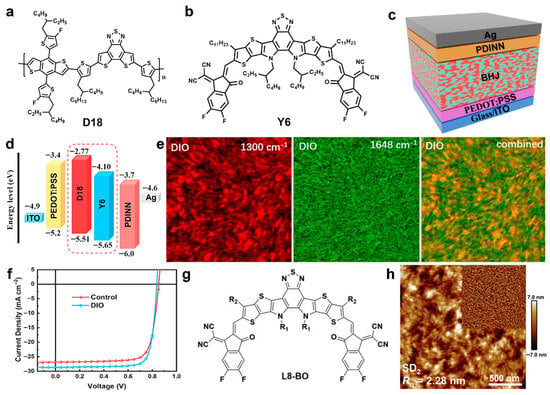
Figure 9.
(a,b) Chemical structure of D18 (a) and Y6 (b). (c) Typical OSC device configuration. (d) Diagram depicting the energy levels of the D18:Y6 BHJ active layer. (e) A series of photo-induced force microscopy (PiFM) images emphasizing the microstructure of a D18:Y6 blend film processed with DIO additive. Here, a wave number of 1300 cm−1 represents Y6 and 1648 cm−1 represents D18, respectively. (f) J-V plots recorded for both control and DIO-processed OSC devices. (g) Chemical structure of L8-BO. (h) AFM height and phase (inset) images depicting the morphology of a D18:L8-BO film obtained after two-step processing via sequential deposition (SD2). Here, Rq refers to the surface roughness. Reproduced from ref. [239] (a–f) [Copyright (2025) Elsevier B.V. All rights are reserved, including those for text and data mining, AI training, and similar technologies, with permission from Elsevier], and ref. [240] (g,h) [Copyright (2022) Wiley-VCH GmbH, with permission from John Wiley and Sons].
Another NFA that has recently gained popularity in the fabrication of polymer:NFA OSCs is the so-called L8-BO. This NFA features a branched 2-butyloctyl alkyl chain and exhibits excellent absorption and packing properties. L8-BO (Figure 9g) has been shown to pair optimally with donor polymers such as D18 [240], MP6 [84], and PMQ-Si605 [241]. The resulting blends—D18:L8-BO, PM6:L8-BO, and PMQ-Si605:L8-BO—were demonstrated to form nanophase-separated ordered morphologies, after appropriate processing, including large nanofibers (Figure 9h) or fibrous structures. The corresponding OSCs exhibited PCEs of 19.05% [240], 19.01% [84], and 18.08% [241], respectively. Moreover, the D18:L8-BO blend was further optimized by modulating the active layer crystallization behavior using D18-Cl as a morphology modulator, which generated a well-structured nanofiber morphology that enhanced both charge separation and carrier transport [242]. The resulting dual-donor OSCs achieved a maximum PCE of 19.13%. This PCE was subsequently surpassed by PCEs recorded in OSCs based on D18:L8-BO blends that were (i) processed under high pressure [243], (ii) composed of both high and low molecular weight D18 [85], or (iii) processed with additives [94]. In the first case, processing the D18:L8-BO blend at elevated temperatures within a pressure-tight vial produced highly crystalline nanofibers with extended exciton diffusion lengths, resulting in a PCE of 19.65% in OSC devices [243]. In the second case, Wei and coworkers utilized both high and low molecular weight D18 donors to construct an ordered multiscale fibrous morphology, MIX-D18:L8-BO. This morphology was characterized by an enlarged exciton diffusion length, improved charge transfer and carrier migration, and reduced trap-assisted recombination, leading to OSCs with an excellent PCE of 20% [85]. In the third case, processing D18 with alkoxythiophene additives and TA yielded an ordered nanophase-separated morphology composed of nanofibrillar structures a few tens of nanometers wide and a few hundred nanometers long, exhibiting a dominant face-on orientation (Figure 10a–i) [94]. Consequently, the resulting D18:L8-BO fibrillar BHJ (Figure 10j,k)) not only promoted an efficient exciton dissociation but also facilitated charge transport, culminating in OSCs with an outstanding PCE of 20.1% [94].
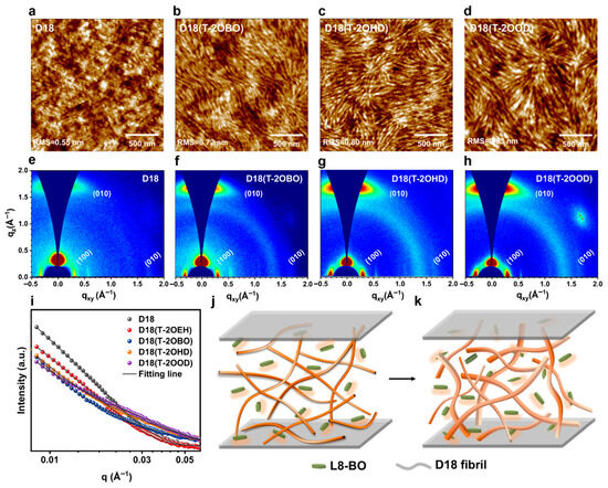
Figure 10.
(a–i) AFM height images (a–d), 2D GIWAXS patterns (e–h), and 1D GISAXS profiles along the qxy axis (i) in D18 films before (a,e) and after processing (b–d,f–h) with T-2OBO (b,f), T-2OHD (c,g), and T-2OOD (d,h) additives. (j,k) Schematic diagram of the obtained morphology displaying thin fibrils in a D18:L8-BO film processed with T-2OEH (j), and thick fibrils in a D18:L8-BO film processed with T-2OOD (k). Reproduced from ref. [94] [Copyright (2024), with permission from the American Chemical Society].
Instead, the PM6:L8-BO blend has recently been successfully utilized at least twice in NFA-based OSCs to further improve the PCE from 19.01% [84] to 19.8% [94], and subsequently to 19.91% [244]. In the first example, PM6:L8-BO was processed with various alkoxythiophene additives and then subjected to TA to generate a nanophase-separated fibrillar morphology, resulting in OSCs with PCEs ranging from 19.3% to 19.8% [94]. In the second case, PM6:L8-BO-X blend was employed. L8-BO-X is a slightly modified version of L8-BO, characterized by a shift in the position of its branched side chains. This blend was processed using reversed TA to induce temperature-modulated nanophase aggregation, which produced honeycomb-like nanostructures. Consequently, while processing the PM6:L8-BO-X blend with conventional TA yielded OSCs with a PCE of 18.98%, using reversed TA increased the PCE of analogous OSCs to 19.91% [94].
Finally, we would like to mention that other efficient polymer:NFA blends have recently been processed using appropriate protocols to fabricate OSCs with PCE in the range of 19.2–19.53%. These include D18:Z19 [92], PBQx-TF:BTP-eC9-2Cl [245], and PM6:BTP-eC9 [246]. In the latter case, adding a dimer acceptor such as QD-1 to the PM6:BTP-eC9 blend can increase the PCE to 20.19%. This high PCE can be further improved to 20.6% by fabricating tandem OSCs [247].
5.3. Nanostructures Leading to High Power Conversion Efficiencies in All-Polymer OSCs
All-polymer OSCs (all-PSCs) have emerged as a promising alternative technology, offering excellent thermal stability, good processability, and relatively high PCEs. These advantages complement their already notable photostability, as well as exceptional device flexibility and stretchability. However, because all-PSCs are composed solely of polymeric materials, a significant drawback is their relatively low electron mobility, especially when compared to that of fullerenes or NFAs. Furthermore, while the molecular arrangements of polymer chains greatly influence the final efficiency of all-PSCs, controlling the microstructure in these systems remains challenging. In contrast, this issue is less pronounced in fullerene- and NFAs-based OSCs, where achieving good control over the blend microstructure is more feasible.
The first all-PSC was fabricated thirty years ago by Yu and Heeger using the donor MEH-PPV and the acceptor cyano--PPV (CN-PPV), achieving a modest PCE of 0.9% [248]. This low efficiency was most likely due to the relatively poor electron mobility of CN-PPV. Once this issue was addressed by designing new polymers (see Section 3 of this work), all-PSCs began to develop rapidly, especially after 2010. By 2018, the PCE of all-PSCs had improved significantly: from just over 1% when combining the donor PTB7 with the acceptor P(NDI2OD-T2) [249], to 5.7% when mixing PBDTTT-EF-T with P(NDI2OD-T2) [250], and exceeding 10% when blending PTzBI-Si with P(NDI2OD-T2) [251]. Subsequently, the morphology of the PTzBI-Si:P(NDI2OD-T2) blend was further optimized by manipulating solvent quality to enhance molecular co-facial packing, resulting in an increased PCE of 11% [252]. Comprehensive summaries of other polymer combinations and the progress of all-PSCs up to 2020 can be found in several detailed reviews available in the literature [134,146,230,253,254].
Between 2020 and 2022, all-PSCs achieved PCEs reaching the 15% limit. For example, Fan and coworkers utilized the donor polymerPBDB-T and a PF5-Y5 polymer to generate a fibrillar microstructure characterized by reduced aggregation and optimized phase separation. This morphology was expected to enhance exciton dissociation and charge transport. Indeed, the measured PCE of PBDB-T:PF5-Y5 all-PSCs was 14.45% [255]. A similar PCE of 14.4% was also achieved by blending PBDB-T with PJ1. The PBDB-T:PJ1 blend exhibited a microstructure consisting of a nanophase-separated interpenetrating network [256]. By optimizing the molecular weight of PBDB-T and subsequently applying TA, Zhang and coworkers improved the microstructure of the PBDB-T:PJ1 blend by enhancing its crystallinity and promoting a face-on orientation of polymer chains within the fibrillar microstructure [257]. This enhancement increased the PCE of PBDB-T:PJ1 solar cells to 15.4%. The PCE of all-PSCs was further improved to 15.8% through the incorporation of a novel narrow-band regioregular polymer acceptor based on benzotriazole (BTz)-core fused-ring segments, named PZT-γ [258]. The resulting morphology of the PBDB-T:PZT-γ active layer consisted of well-defined, phase-separated fibrous interpenetrating structures of optimal size, which promoted efficient exciton dissociation and effective charge transport [258].
Surpassing the 16% PCE threshold was achievable only in ternary all-PSCs utilizing the PM6 donor. This was accomplished either by combining PM6 with various electron acceptors, such as regioregular L15 and MBTI—synthesized through the copolymerization of dibrominated fused-ring electron acceptors with distannylated aromatic imide [259]—or by employing other donor:acceptors pairs, including PTQ10:PY-IT [260] and J71:PY-IT [261]. The highest PCEs obtained for these nanoscale phase-separated microstructures were 16.5% for the M6:L15:MBTI ternary blend [259], and 16.52% for the PM6:PTQ10:PY-IT [260] and PM6:J71:PY-IT blends [261].
Since 2023, various polymeric systems have been successfully employed to develop highly efficient donor-acceptor blends capable of achieving PCEs exceeding 19% in binary configurations [262]. Notably, all-PSCs with PCEs surpassing 17% were first reported for nanofibrillar morphologies, which promote binary exciton dissociation and enhance charge transport. These blends were created by mixing either the donor PBQx-TCl with the acceptor BTPICγ-BDD [263], or the donor PBBTz-Cl with the acceptor PY-IT [264]. It is important to note that the donor PBQx-TCl results from the copolymerization of a chlorinated BDT-T unit with DTQx; PBBTz-Cl is a polymer synthesized by connecting the benzobisthiazole and chlorinated benzodithiophene units with thiophene, and BTPICγ-BDD is based on the copolymerization of a BDD unit with an Y-shaped small NFA.
Moreover, the PM6 donor (Figure 11a) appears to be the best match for PY-IT (Figure 11b), as demonstrated by the impressive device performance of all-PSC devices made from PM6:PY-IT blends (Figure 11c,d), with PCEs reaching up to 19.06% [262]. This record PCE was achieved by Zeng and coworkers, who (i) enhanced light collection by using a micro-sized surface topology and (ii) optimized the active layer by combining SVA with TA and the use of additives to control the kinetics of polymer crystallization. Through this processing, they generated a nano-to-micron sized hierarchical morphology composed of interconnected nanofibrillar donor-acceptor networks of molecular dimensions (Figure 11e,f) [262]. This morphology not only facilitated efficient photon-to-charge conversion, but also enabled a large light-receiving angle, resulting in a 30% increase in power output [262]. This record PCE of over 19% for binary (and ternary) all-PSCs (Figure 11d) was recently surpassed, approaching 20%, but only in all-PSCs based on multicomponent blends [83,265]. For example, Wang and coworkers diluted PM6 with PY-IT and subsequently diluted PY-IT with PM6 or D18 to generate highly structured donor-dominant or acceptor-dominant heterojunctions that enhanced charge carrier mobility and improved exciton diffusion length. These blends exhibited PCEs ranging from 18.8% to 19.4% [265]. Another example of multicomponent all-polymer blends was reported by Wu and coworkers, who employed a layer-by-layer (LbL) doctor-blading deposition technique to fabricate a quaternary PM6:D18-Cl:PY-SSe:PY-Cl structure. This architecture not only improved charge transfer and transport but also reduced losses caused by non-geminate recombination [83]. Consequently, all-PSCs based on LbL-processed PM6:D18-Cl:PY-SSe:PY-Cl structures achieved maximum PCEs of 19.46%, whereas their BHJ analogs exhibited lower PCEs of only 16.02% [83].
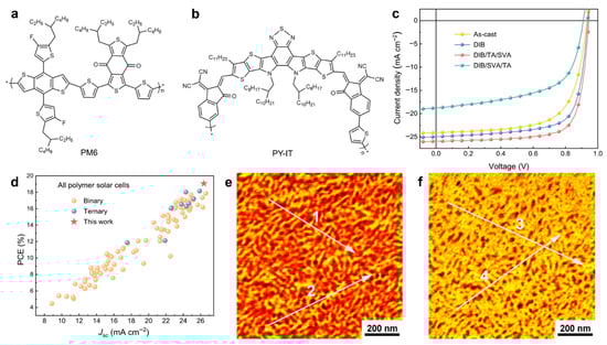
Figure 11.
(a,b) Chemical structure of PM6 (a) and PY-IT (b). (c) J-V curves of all-PSCs processed in various conditions and measured under AM 1.5 G (100 mA/cm2). Here, DIB stands for the 1,4-diiodobenzene additive. (d) Comparison of the PCE versus JSC for the most prominent all-PSCs reported in the literature until 2023. (e,f) Tapping AFM-based infrared spectroscopy micrographs recorded at the wavenumber of 1650 cm−1 (representing PM6) and 2215 cm−1 (representing PY-IT) for PM6:PY-IT blend films processed with DIB and exposed to TA and SVA. White arrows and numbers are not relevant here. Reproduced from ref. [262] [Copyright (2023) the author(s), with permission from Springer Nature].
Finally, it is important to note that thermal stability remains a critical challenge for organic energy devices due to the inherently heat-sensitive nature of organic materials. Consequently, while polymer materials can degrade upon annealing at elevated temperatures, small semiconducting molecules may undergo volatilization and thermal oxidation. Moreover, both types of materials can experience morphological instabilities and changes in crystallinity, which may alter the microstructure and reduce the optoelectronic performance. For example, drawbacks of TA include electrode instabilities caused by the diffusion of metal atoms at high temperatures, unwanted interlayer reactions driven by thermal energy, and limited operational lifetimes, as organic energy devices exhibit performance degradation when subjected to prolonged TA at elevated temperatures. Potential solutions to these issues include the use of thermally stable materials (for example, polymers with high glass transition temperatures) and crosslinking polymer chains through chemical bonding.
Table 3.
Summary of recent, most relevant photovoltaic properties reported in the literature for various types of OSCs. Most relevant values are marked in gray.
Table 3.
Summary of recent, most relevant photovoltaic properties reported in the literature for various types of OSCs. Most relevant values are marked in gray.
| Donor:acceptor | Polymer Molecular Weight (kg/mol) | Nanostructure Type | Processing Method | JSC (mA/cm2) | FF (%) | VOC (V) | PCE (%) | Ref. |
|---|---|---|---|---|---|---|---|---|
| Fullerene-based OSCs | ||||||||
| P3HT:PC71BM | Mn = 7.15 | single crystal | solution grown crystals/nanofibers were mixed with PC71BM and spin coated to fabricate thin films | 7.69 | 54 | 0.59 | 2.45 | [232] |
| P3HT:PC71BM | Mn = 7.15 | nanofiber | 5.93 | 45 | 0.57 | 1.52 | [232] | |
| P3HT:PC71BM | Mn = 48.8 | single crystal | 9.18 | 55 | 0.58 | 2.93 | [232] | |
| P3HT:PC71BM | Mn = 48.8 | nanofiber | 7.10 | 47 | 0.59 | 1.97 | [232] | |
| P3HT-b-PEG:PC71BM | Mn = 49.55 | hairy single crystal | 9.26 | 54 | 0.58 | 2.90 | [232] | |
| P3HT-b-PEG:PC71BM | Mn = 49.55 | nanofiber | 7.11 | 53 | 0.58 | 2.18 | [232] | |
| P3HT-b-PS:PC71BM | Mn = 7.669 | hairy single crystal | 7.74 | 51 | 0.58 | 2.29 | [232] | |
| P3HT-b-PMMA:PC71BM | Mn = 7.647 | hairy nanofiber | 5.47 | 47 | 0.58 | 1.49 | [232] | |
| PffBT4T-C9C13:PC71BM | - | 38 nm polymer-rich domains comprising molecules adopting face-on orientations | spin coating from warm solutions | 19.8 | 73 | 0.784 | 11.7 | [93] |
| PM6:BTP-eC9:PC71BM multicomponent | - | ~35 nm long nanofiber-like structures | spin coating solutions containing DQ | 26.93 | 79.4 | 0.856 | 18.3 | [234] |
| OSCs based on non-fullerene acceptors | ||||||||
| PBDB-T-SF:IT-4F | Mn = 20.9 | nanophase-separated morphology | spin coating | 20.88 | 71.3 | 0.88 | 13.1 | [236] |
| PM6:Y6 | - | morphology comprising homogeneous nanophase | processed with BDT additive, TA | 27.61 | 77.11 | 0.841 | 17.91 | [84] |
| D18:Y6 D18-Cl:Y6 | - | small and homogeneous aggregation domains | processed with DBTF and DBOF additives, TA | 27.65 | 77.99 | 0.890 | 19.19 | [238] |
| D18:Y6 | - | nanophase-separated morphology comprising nanofibril networks | synergistically dual-phases morphology control | 28.6 | 80.84 | 0.836 | 19.35 | [239] |
| D18:L8-BO | - | 20 nm large nanofibers | spin coating sequential deposition | 26.86 | 77.25 | 0.918 | 19.05 | [240] |
| PM6:L8-BO | - | morphology comprising homogeneous nanophase | processed with BDT additive, TA | 26.59 | 80.03 | 0.893 | 19.01 | [84] |
| PMQ-Si605 | Mn = 51.1 | phase-separated fibrous structures | spin coating and TA | 26.16 | 77.40 | 0.893 | 18.08 | [241] |
| D18:L8-BO | Mn = 84.5 | highly crystalline nanofibers | high-pressure fabrication in a pressure-tight vial | 26.48 | 80.65 | 0.910 | 19.65 | [243] |
| MIX-D18:L8-BO | Mn ≥ 40/<40 | multiscale interpenetrating fiber network structure | spin coating and TA | 26.75 | 81 | 0.920 | 20.0 | [85] |
| D18:L8-BO | - | morphology comprising nanofibril aggregates with dominant face-on orientation | processed with alkoxythiophene additives, TA | 26.5 | 81.2 | 0.906 | 20.1 | [94] |
| PM6:L8-BO | - | phase-separated nanofibrillar morphology | processed with alkoxythiophene additives, TA | 26.8 | 80.20 | 0.902 | 19.8 | [94] |
| PM6:L8-BO-X | - | nanophase-aggregated honeycomb resembling nanostructures | reversed TA | 28.12 | 79.46 | 0.891 | 19.91 | [94] |
| D18:Z19 | - | phase-separated fibrous morphology with preferential face-on orientation | spin coating and TA | 24.6 | 77.60 | 1.002 | 19.2 | [92] |
| PBQx-TF:BTP-eC9-2Cl | - | phase-separated fibrillar network with face-on orientation | processed with additives, TA | 27.2 | 80.40 | 0.879 | 19.2 | [245] |
| PM6:BTP-eC9 PM6:BTP-eC9:QD-1 | Mn = 45 | interpenetrating phase-separated fiber-like network structures | spin coating and TA | 28.51 28.98 | 79.30 79.82 | 0.864 0.873 | 19.53 20.19 | [246] |
| All polymer OSCs | ||||||||
| f-BTI2-FT:PTB7-Th | Mn = 13.8/- | phase-separated bicontinuous network | TA | 11.55 | 57.04 | 1.04 | 6.85 | [170] |
| PTzBI-Si:P(NDI2OD-T2) | Mn = 38.4/75.1 | phase-separated crystalline morphology with preferential face-orientation | spin coating and TA | 15.57 | 73.39 | - | 10.1 | [251] |
| PBDB-T:PF5-Y5 | Mw = -/33.3 | fibral microstructures | spin coating and TA | 20.65 | 74 | 0.946 | 14.45 | [255] |
| PBDB-T:PJ1 | Mn = -/23.3 | finely nanoscale phase-separated interpenetrating network | spin coating and TA | 22.3 | 70 | 0.9 | 14.4 | [256] |
| PBDB-T:PJ1 | Mn = 38/11.4 | fibril-like nanostructures with preferential face-on orientation | spin coating and TA | 22.7 | 75.3 | 0.9 | 15.4 | [257] |
| PBDB-T:PZT-γ | Mn = -/7.8 | phase-separated fibrous interpenetrating nanostructures | solvent optimization, spin coating and TA | 24.7 | 71.3 | 0.896 | 15.8 | [258] |
| PBBTz-Cl:PY-IT | Mn = 61.3/- | nanofibrillar D-A structures | spin coating and TA | 24.56 | 73.73 | 0.947 | 17.15 | [264] |
| PBQx-TCl:BTPICγ-BDD | Mn = -/12.38 | nanofibrillar D-A structures | spin coating and TA | 24.1 | 76.92 | 0.944 | 17.5 | [263] |
| PM6:PY-IT | - | interconnected nanofibrillar D-A networks | spin coating combined with SVA, TA, use of additives and topologically modified surfaces | 26.37 | 76.48 | 0.945 | 19.06 | [262] |
6. Conclusions
In this review, we link the most relevant nanostructures fabricated in recent years from semiconducting polymers—using a variety of processing protocols—to their final optoelectronic properties (e.g., charge mobility, electrical conductivity, photovoltaic capabilities) measured in specific energy devices. We observe that ordered nanowires of PCDTPT, fabricated via liquid-bridge-mediated nano-transfer molding, exhibit the highest charge mobility among all semiconducting polymers (µ = 92.64 cm2V−1s−1, ref. [96]; note that ladder-type 2DCPs, excluded from this work, have demonstrated charge mobilities up to 970 cm2V−1s−1, ref. [169]). This dominance is shared by nanowires of DPPBTSPE, which show a hole mobility of 24 cm2V−1s−1 (ref. [29]), the highest value recorded for a DPP-based system. It is also noteworthy that nanofibers and fiber-like polycrystalline grains made of IID-based polymers can achieve efficient charge mobilities, with hole and electron mobilities reaching 14.4 cm2V−1s−1 and 9.7 cm2V−1s−1, respectively (refs. [95] and [149]). Furthermore, the highest electron mobility is that reported for F4BDOPV-2T structures (14.9 cm2V−1s−1, ref. [153]). In contrast, the highest mobilities for common polythiophene polymers remain those measured in highly ordered single crystals of P3OT (0.62 cm2V−1s−1, ref. [126]) and P3HT (0.5 cm2V−1s−1, ref. [90]). Finally, it is worth mentioning that charge mobilities can be significantly enhanced by chemical doping (for example, PEDOT doped with FeCl3 achieved mobilities exceeding 33 cm2V−1s−1, ref. [164]) and by blending with other polymers (for instance, nanofibers of PCDTPT mixed with PS experienced a hole mobility of 23.7 cm2V−1s−1, ref. [157]).
PEDOT fibrillar domains, displaying a face-on orientation and fabricated using the oCVD method combined with acid treatment, have achieved the highest electrical conductivity reported for a semiconducting polymer to date (6259 S/cm, ref. [182]). This conductivity significantly surpasses that of PANI self-assembled nanotubes (320 S/cm, ref. [220]) and that of ordered edge-on oriented crystalline structures of selenium-substituted DPP (977 S/cm, ref. [194]). Nanofibers of PEDOT:PSS, obtained by mixing PEDOT with the non-conductive PSS and processed via a solution shearing approach, exhibit a lower conductivity (4600 S/cm, ref. [187]) compared to the highest values recorded for PEDOT. However, this conductivity can be substantially increased to over 5000 S/cm by employing additives (ref. [188]). Furthermore, similar to charge mobility, electrical conductivity can be enhanced through chemical doping. For instance, doping a PBTTT derivative with FeCl3, combined with doctor blading, high-temperature film rubbing, and TA, produced π-stacked ordered domains of highly aligned polymer chains intercalated with dopants, resulting in an exceptional electrical conductivity of 2.2 × 10⁵ S/cm (ref. [205]).
The photovoltaic properties of semiconducting polymer-based nanostructures were summarized considering three main classes of OSCs. The first class, fullerene-based OSCs, has reached its performance limit in terms of PCE. For example, PffBT4T-C9C13:PC71BM OSCs fabricated from a BHJ comprising polymer-rich domains several tens of nanometers in size with molecules adopting face-on orientations, achieved a PCE of 11.7% (ref. [93]). Higher PCE values have only been reported for multicomponent OSCs, with the highest PCE of 18.3% observed in long PM6:BTP-eC9:PC71BM nanofiber-like structures containing DQ (ref. [234]). The second class, OSCs based on NFAs, has proven more versatile, with typical PCEs ranging from approximately 17% to just under 20%. Two recent studies demonstrated that D18:L8-BO multiscale interpenetrating fiber network structures and nanofibril aggregates with dominant face-on orientation, processed using alkoxythiophene additives, yielded OSCs with PCEs of 20% (ref. [85]) and 20.1% (ref. [94]), respectively. A higher PCE of 20.19% was recently achieved in OSCs based on interpenetrating phase-separated fiber-like network structures composed of PM6:BTP-eC9 blends containing additional dimer acceptors (resulting PCE = 20.19%, ref. [246]). It is also noteworthy that the VOC of 1.002V measured in OSCs with D18:Z19 phase-separated fibrous morphology (ref. [92]) appears to be the highest reported to date. Finally, the third class comprises all-PSCs. Although reported PCEs for all-PSCs typically range between 15% and just under 18%, a breakthrough morphology consisting of PM6:PY-IT interconnected nanofibrillar D-A networks—fabricated by combining spin coating with SVA and TA, while employing additives and topologically modified surfaces—achieved a record PCE exceeding 19% (ref. [262]).
Author Contributions
Conceptualization, I.B. and M.P.; methodology, I.B. and M.P.; formal analysis, I.B. and M.P.; data curation, I.B. and M.P.; writing—original draft preparation, M.P.; writing—review and editing, I.B.; supervision, I.B. All authors have read and agreed to the published version of the manuscript.
Funding
This research received no external funding.
Data Availability Statement
Not applicable.
Acknowledgments
M. P. acknowledges the financial support from the doctoral grant offered by the Babes-Bolyai University.
Conflicts of Interest
The authors declare no conflicts of interest.
Abbreviations
| 2DCP-MPc | 2D phthalocyanine-based poly(benzimidazobenzophenanthroline); |
| 2DCPs | two-dimensional conjugated polymers; |
| BDD | 1,3-bis(thiophen-2-yl)-5,7-bis(2-ethylhexyl)benzo-[1,2-c:4,5-c′]dithiophene-4,8-dione; |
| BDT | benzo [1,2-b:4,5-b′]dithiophene; |
| BFDO | benzodifurandione; |
| BHJ | bulk heterojunction; |
| BPE | branched polyethylene; |
| BTBT | (di)thiophene, [1]benzothieno[3,2-b][1]benzothiophene; |
| BTP-eC9 | 2,2′- [[12,13-Bis(2-butyloctyl)-12,13-dihydro-3,9 dinonylbisthieno[2″,3″:4′,5′]thieno[2′,3′:4,5] pyrrolo[3,2-e:2′,3′-g][2,1,3]benzothiadiazole-2,10-diyl]bis[methylidyne(5,6-chloro-3-oxo-1H-indene-2,1(3H)-diylidene)]]bis [propanedinitrile]; |
| BTP-eC9-2Cl | 2,2′- [[12,13-Bis(2-butyloctyl)-12,13-dihydro-3,9-dinonylbisthieno[2″,3″:4′,5′] thieno[2′,3′:4,5]pyrrolo[3,2-e:2′,3′-g][2,1,3]benzothiadiazole-2,10-diyl]bis[methylidyne(2 or 3-chloro-3-oxo-1H-indene-2,1(3H)-diylidene) ]]bis [propanedinitrile]; |
| C-AFM | conductive atomic force microscopy; |
| CDT | cyclopentadithiophene; |
| CDT-BTZ | polymer based on ecosyl-substituted cyclopentadithiophene-benzothiadiazole; |
| CN6-CP | hexacyano-trimethylene-cyclopropane; |
| CoCp2 | bis(cyclopentadienyl)cobalt; |
| CPE | conjugated polyelectrolyte; |
| D-ODCB | deuterated 1,2 dichlorobenzene; |
| D-A | donor-acceptor; |
| D18 | poly[(2,6-(4,8-bis(5-(2-ethylhexyl)-4-fluoro)thiophen-2-yl)-benzo[1,2-b:4,5-b′]dithiophene)-alt-5,5′-(5,8-bis(4-(2-butyloctyl)thiophen-2-yl)dithieno [3′,2′:3,4;2″,3″:5,6] benzo [1,2-c][1,2,5]thiadiazole)]; |
| D18-Cl | poly[(2,6-(4,8-bis(5-(2-ethylhexyl)-4-chlorothiophen-2-yl)-benzo[1,2-b:4,5-b′]dithiophene))-alt-5,5′-(5,8-bis(4-(2-butyloctyl)thiophen-2-yl)dithieno[3′,2′:3,4;2″,3″:5,6]benzo[1,2-c][1,2,5]thiadiazole)]; |
| DBOF | 3,5-dibromotriffluoromethoxybenzene; |
| DBTF | 3,5-dibromobenzotrifluoride; |
| DBTTT | dibenzothiopheno[6,5-b:6′,5′-f]thieno[3,2-b]thiophene; |
| DDB | dodecaborane; |
| DFSe | diketopyrrolopyrrole-difluorobenzoselenadiazole-diketopyrrolopyrrole; |
| DIO | 1,8-diiodooctane; |
| DMSO | dimethyl sulfoxide; |
| DNTT | dinaphtho[2,3-b:2′,3′-f]thieno[3,2-b]thiophene; |
| DPP | diketopyrrolopyrrole; |
| DPP-2T | a polymer based on DPP and containing bithiophene; |
| DPPBTSPE | is based on DPP and 1,2-bis(5-(thiophen-2-yl)selenophen-2-yl)ethene (BTSPE); |
| DPPF-NTz | a polymer made of a furan-flanked diketopyrrolopyrrole (DPPF) as a monomer and napthobisthiadiazole (NTz) as comonomer units; |
| DTQx | dithieno[3,2-f:2′,3′-h]quinoxaline; |
| EMIM TFSI | 1-ethyl-3-methylimidazolium bis(trifluoromethylsulfonyl) imide; |
| F4BDOPV-2T | a polymer composed of four-fluorinated benzodifurandione-based oligo(p-phenylene vinylene) (F4BDOPV) and 2,2′-bithiophene; |
| F4TCNQ | 2,3,5,6-tetrafluoro-7,7,8,8-tetracyanoquinodimethane; |
| F8T2 | poly(9,9-dioctylfuorene-co-bithiophene); |
| FBDPPV | a polymer system derived from fluorinated benzodifurandione (FBD); |
| FBDPPV-OEG | a polymer which incorporates oligo(ethylene glycol) (OEG)-substituted FBD; |
| Fe(OTf)3 | iron(III) trifluoromethanesulfonate; |
| f-BSeI2TEG-FT | a polymer system obtained by selenium substitution in bithiophene imide; |
| f-BTI2-FT | a polymer based on a fused bithiophene imide (BTI); |
| f-BTI2TEG-T and f-BTI2TEG-FT | polymers comprising f-BTI2 bearing 3-(2-(2-methoxyethoxy)ethoxy)-2-((2-(2-methoxyethoxy)ethoxy)methyl)propan-1-yl side chain as the acceptor unit and thiophene/difluorothiophene as the donor co-unit (fluorine F atoms were introduced to further tune polymers′ frontier molecular orbital energy levels and crystallinity; f-fused); |
| GIWAXS | grazing incidence wide-angle X-ray scattering; |
| H2SO4 | sulfuric acid; |
| HDPE | high-density polyethylene; |
| HOMO | highest occupied molecular orbital; |
| HOMPP | 2-hydroxy-2-methyl propiophenone; |
| ID | drain current; |
| IDT | indacenodithiophene; |
| IDTT | indacenodithieno[3,2-b]thiophene; |
| IDTz | indacenodithiazole; |
| IID | isoindigo; |
| IT-4F | 3,9-bis(2-methylene-((3-(1,1-dicyanomethylene)-6,7-difluoro)-indanone))-5,5,11,11-tetrakis(4-hexyl phenyl)-dithieno[2,3-d:2′,3′-d′]-s-indaceno[1,2-b:5,6-b′]dithiophene; |
| ITIC | 3,9-bis(2-methylene-(3-(1,1-dicyanomethylene)-indanone))-5,5,11,11-tetrakis(4-hexylphenyl)-dithieno[2,3-d:2′,3′-d′]-s-indaceno[1,2-b:5,6-b′]dithiophene; |
| J71 | poly[[5,6-difluoro-2-(2-hexyldecyl)-2H-benzotriazole-4,7-diyl]-2,5-thiophenediyl[4,8-bis[5-(tripropylsilyl)-2-thienyl]benzo[1,2-b:4,5-b′]dithiophene-2,6-diyl]-2,5-thiophenediyl]; |
| L8-BO (also known as L8-BO-2F) | 2,2′-((2Z,2′Z)-((12,13-bis(2-ethylhexyl)-3,9-(2-butyloctyl)-12,13-dihydro-[1,2,5] thiadiazolo[3,4-e]thieno[2″,3″:4′,5′]thieno[2′,3′:4,5]pyrrolo[3,2-g]thieno[2′,3′:4,5]thieno[3,2-b]indole-2,10-diyl)bis (methanylylidene))bis(5,6-difluoro-3-oxo-2,3-dihydro-1H-indene-2,1-diylidene))dimalononitrile; |
| LUMO | lowest unoccupied molecular orbital; |
| MEH-PPV | poly[2-methoxy-5-(2-ethylhexyloxy)-1,4-phenylenevinylene]; |
| N-DMBI | 4-(1,3-dimethyl-2,3-dihydro-1H-benzoimidazol-2-yl)-N,N-dimethylaniline; |
| n-PT4 | a polymer system created by functionalizing each thiophene unit of a non-fused-ring polythiophene backbone with imide or cyano groups; |
| NFA | non-fullerene acceptor; |
| NDI | naphthalenediimide; |
| NH-FDPP-BT | fluorene-flanked diketopyrrolopyrrole (FDPP)-based semiconducting polymers containing bithiophene (BT) as the donor comonomers; |
| NH-FDPP-TT | fluorene-flanked diketopyrrolopyrrole (FDPP)-based semiconducting polymers containing thieno[3,2-b]thiophene (TT) as the donor comonomers; |
| NTz | napthobisthiadiazole; |
| oCVD | oxidative chemical vapor deposition; |
| OECTs | organic electrochemical transistors; |
| OFETs | organic field-effect transistors; |
| OLEDs | organic light-emitting diodes; |
| OSCs | organic solar cells; |
| P(g2T-T) | poly(2-(3,3′-bis(2-(2-(2-methoxyethoxy)ethoxy)ethoxy)-[2,2′-bithiophen]-5)yl thiophene); |
| P(g2T-TT) | poly(2--(3,3′--bis(2--(2--(2--methoxyethoxy)ethoxy)ethoxy)--[2,2′--bithiophen]--5--yl)thieno 3,2--b] thiophene); |
| P(gDPP-MeOT2), P(gDPP-T2) and P(gDPP-TT) | D-A copolymers based on 3,6-bis(5-bromothiophen-2-yl)-2,5-bis(2-(2-(2-methoxyethoxy)ethoxy) ethyl)-2,5dihydropyrrolo [3,4-c]pyrrole-1,4-dione; |
| P(gT2) | poly-[3,3′-bis(2-(2-(2-methoxyethoxy)ethoxy)ethoxy)-2,2′-bithiophene]; |
| P(DPP-CNPz) | a polymer based on 3,6-dibromopyrazine-2-carbonitrile (CNPz); |
| P(DPP-DCNPz) | a polymer based on 3,6-dibromopyrazine-2,5-di-carbonitrile (DCNPz); |
| P(DPP-T) | poly(diketopyrrolopyrrole-co-thiophene); |
| P(NDI2OD-Se-Th 1.0) | poly[4-methyl-9-(5-(5-(9-(5-methylselenopheno[3,2-b]thiophen-2-yl)-2,7-bis(2-octyldodecyl)-1,3,6,8-tetraoxo-1,2,3,6,7,8-hexahydrobenzo[lmn][3,8]-phenanthrolin-4-yl)selenophen-2-yl)thiophen-2-yl)-2,7-bis(2-octyldodecyl)benzo[lmn][3,8]phenanthroline -1,3,6,8(2H,7H)-tetraone]; |
| P(NDI2OD-T2) or N2200 | poly{[N,N′-bis(2-octyldodecyl)-1,4,5,8-naphthalene diimide-2,6-diyl]-alt-5,5′-(2,2′-bithiophene)}; |
| P(NDI2SiC6-T2) | a polymer composed of naphthalenediimide and bithiophene (T2) repeating units; |
| P(PzDPP-2FT) | a polymer featuring pyrido[3,4-b]pyrazine-diketopyrrolopyrrole (PzDPP) units and fluorinated bithiophene (2FT) blocks; |
| P(TDPP-BBT) | a D-A polymer based on thiophene-flanked diketopyrrolopyrrole and benzobisthiadiazole (BBT); |
| P(TDPP-BT) | a D-A polymer based on thiophene-flanked diketopyrrolopyrrole and benzothiadiazole (BT); |
| P(TDPP-TQ) | a D-A polymer (see its chemical structure in the inset) based on thiophene-flanked DPP and thymoquinone (TQ); |
| P(TzII-dTh-dTh) | a polymer synthesized by copolymerizing thiophene-flanked thiazoloisoindigo (TzII) with bithiophene; |
| P(TzII-dTh-dTz) | a polymer synthesized by copolymerizing thiophene-flanked TzII with bithiazole; |
| P2TDPP2TFT4 | poly[((2,6--bis(thiophen--2--yl)--3,7--bis(9--octylnonadecyl)thieno[3,2--b]thieno[2′,3′:4,5] thieno[2,3--d]thiophene)--5,5′--diyl)(2,5--bis(8--octyl octadecyl)--3,6--di(thiophen--2--yl)pyrrolo[3,4--c]pyrrole--1,4--dione)--5,5′--diyl]]; |
| P3HT | poly(3-hexylthiophene); |
| P3HT-b-PDL | poly(3-hexylthiophene)-block-poly(δ-decanolactone); |
| P3OT | poly(3-octylthiophene); |
| PA | polyacetylene; |
| PANI and TANI | polyaniline and tetraaniline; |
| PB | polybutadiene; |
| PBDB-T | poly[(2,6-(4,8-bis(5-(2-ethylhexyl)thiophen-2-yl)-benzo[1,2-b:4,5-b′]dithiophene))-alt-(5,5-(1′,3′-di-2-thienyl-5′,7′-bis(2-ethylhexyl)benzo[1′,2′-c:4′,5′-c′]dithiophene-4,8-dione))]; |
| PBDB-T-SF | poly[(2,6-(4,8-bis(5-(2-ethylhexylthio)-4-fluorothiophen-2-yl)-benzo[1,2-b:4,5-b′]dithiophene))-alt-(5,5-(1′,3′-di-2-thienyl-5′,7′-bis(2-ethylhexyl)benzo[1′,2′-c:4′,5′-c′]dithiophene-4,8-dione)]; |
| PBDP-F2 | a polymer based on 3-dodecylthiophene-flanked (BDP) as the electron-acceptor moiety and thiophene derivatives containing fluorine atoms as electron-donor moieties; |
| PBDTTT-EF-T | poly[[4,8-bis[5-(2-ethylhexyl)-2-thienyl]benzo[1,2-b:4,5-b′]dithiophene-2,6-diyl][2-[[(2-ethylhexyl)oxy] carbonyl]-3-fluorothieno[3,4-b]thiophenediyl]]; |
| PBFDO | poly(benzodifurandione); |
| PBQx-TF | a polymer that results from the copolymerization of a fluorinated benzo[1,2-b:4,5-b′]dithiophene (BDT-T) unit with dithieno[3,2-f:2′,3′-h]quinoxaline (DTQx); |
| PBTTT | poly(2,5-bis(3-alkylthiophen-2-yl)thieno[3,2-b]thiophene); |
| PCBM | phenyl-C61-butyric acid methyl ester; |
| PCE | power conversion efficiency; |
| PCDTPT | poly[4-(4,4-dihexadecyl-4H-cyclopenta [1,2-b:5,4-b′]dithiophen-2-yl)-alt-[1,2,5]thiadiazolo[3,4-c]pyridine]; |
| PCDTPT-ODD | poly[4-(4,4-bis(2-octyldodecyl)-4H-cyclopenta[1,2-b:5,4-b′]dithiophen-2-yl)-alt-[1,2,5]-thiadiazolo [3,4-c]pyridine]; |
| PCNI2-BTI | a polymer based on a cyano-functionalized fused bithiophene imide dimer; |
| PDFDSe | poly(4-(4,4-bis(2-ethylhexyl)-4H-silolo[3,2-b:4,5-b′]dithiophene-2-yl)-7-(4,4-bis(2-ethylhexyl)-6-(selenophene-2-yl)-4H-silolo[3,2-b:4,5-b′]dithiophene-2-yl)-5,6-difluorobenzo[c][1,2,5]thiadiazole; |
| PDMS | poly(dimethylsiloxane); |
| PDPP-DTT | polydiketopyrrolopyrrole-dithienylthieno[3,2-b]thiophene; |
| PDPP-TT-PDMS | poly-diketopyrrolopyrrole-thienothiophene-poly(dimethylsiloxane); |
| PDPP-TVT | poly[2,5-bis(2-decyltetradecyl)pyrrolo[3,4-c]pyrrole-1,4-(2H,5H)-dione-(E)-1,2-di(2,20-bithiophen-5-yl) ethene]; |
| PDPP3T | poly(diketopyrrolopyrroleterthiophene); |
| PDPIN | a polymer based on the 2,2′-((2E,2′E)-(((2,5-bis(2-octyldodecyl)-3,6-dioxo-2,3,5,6-tetrahydropyrrolo[3,4-c] pyrrole-1,4-diyl)bis(thiophene-5,2-diyl))bis(methanylylidene))bis(3-oxo-2,3-dihydro-1H-indene-2,1-diylidene))dimalononitrile repeat unit; |
| PDPPT3 | poly{2,2′-[(2,5-bis(2-hexyldecyl)-3,6-dioxo-2,3,5,6- tetrahydropyrrolo[3,4-c]pyrrole-1,4-diyl)dithiophene]- 5,5′-diyl-alt-thiophen-2,5-diyl}; |
| PDPPT325% | poly(2,5-bis (4-hexyldodecyl)-2,5-dihydro-3,6-di-2-thienyl-pyrrolo[3,4-c] pyrrole-1,4-dionealt-thiophene); |
| PDPPy-Se | a polymer based on pyridine and selenophene; |
| PDTTDPP | a copolymer composed of DPP and dithieno[3,2-b:20,30-d]thiophene (DTT); |
| PDTzSI-Se | a polymer which is based on thiazole imide with a high content of selenophene; |
| PEDOT | poly(3,4-ethylenedioxythiophene); |
| PE | polyethylene; |
| PEGDA | poly(ethylene glycol) diacrylate; |
| PF5-Y5 | a polymer synthesized by coupling a (2,2′-((2Z,2′Z)-((12,13-bis(2-ethylhexyl)-3,9-diundecyl-12,13-dihydro[1,2,5]thiadiazolo[3,4e]thieno[2″,3″:4′,5′] thieno[2′,3′:4,5]pyrrolo[3,2-g] thieno[2′,3′:4,5]thieno[3,2-b]indole-2,10-diyl)bis(methanylylidene))bis(3-oxo-2,3-dihydro1H-indene-2,1-diylidene))dimalononitrile) (Y5) acceptor unit with a thienyl-benzodithiophene (BDT-T) donor unit; |
| PFClTVT | a polymer based on dichlorodithienylethene (ClTVT); |
| PffBT4T-C9C13 | poly[(5,6-difluoro-2,1,3-benzothiadiazol-4,7-diyl)-alt-(3,3″′- di(2-nonyltridecyl)-2,2′;5′,2″;5″,2″′-quaterthiophen-5,5″′-diyl)]; |
| PFO | poly(9,9-dioctylfluorene); |
| PgBTTT | a polymer obtained by relocating the glycol side chains position on the bithiophene unit of poly(2--(3,3′--bis(2--(2--(2--methoxyethoxy)ethoxy)ethoxy)--[2,2′--bithiophen]--5--yl)thieno 3,2--b] thiophene); |
| PJ1 | poly[[12,13-bis(2-decyltetradecyl)-12,13-dihydro-3,9 diundecylbisthieno[2″,3″:4′,5′]thieno[2′,3′:4,5]pyrrolo[3,2-e:2′,3′-g][2,1,3]benzothiadiazole-2,10-diyl]methylidyne[1-(dicyanomethylene)-1,3-dihydro-3-oxo-2H-inden-yl-2-ylidene]-2,5-thiophenediyl[1-(dicyanomethylene)-1,3-dihydro-3-oxo-2H-inden-yl-2-ylidene]methylidyne]; |
| PM6 (also known as PBDB-T-2F) | poly[(2,6-(4,8-bis(5-(2-ethylhexyl)-4-fluorothiophen-2-yl)-benzo[1,2-b:4,5-b′]dithiophene))-alt-(5,5-(1′,3′-di-2-thienyl-5′,7′-bis(2-ethylhexyl)benzo[1′,2′-c:4′,5′-c′]dithiophene-4,8-dione))]; |
| PMMA | poly(methyl methacrylate); |
| PMQ-Si605 | a polymer based on 6,7-difluoro-3-methylquinoxaline-thiophene backbone and containing 5% siloxane; |
| PNBDO-FDTE | poly((3E,7E)-3,7-bis(2-oxo-1Hpyrrolo[2,3-b]pyridin-3(2H)-ylidene)benzo[1,2-b:4,5-b′]-difuran-2,6 (3H,7H)-dione)-(E)-1,2-bis(3-fluorothiophen-2-yl)ethene; |
| PNDI-RO | a polymer consisting of p-conjugated backbones adjacent to alkyl chains; |
| PNDI2TEG-2Tz | a polymer system synthesized using bithiazole/2Tz donor units and NDI carrying triethylene glycol acceptors; |
| PNDIF-T2 | poly[2,7-bis(11,11,12,12,13,13,14,14,15,15,16,16,17,17,18,18,18-heptadecafluoro octadecyl)-4-methyl-9-(5′-methyl-[2,2′-bithiophen]-5-yl)benzo[lmn][3,8]phenanthroline-1,3,6,8 (2H,7H)-tetraone]; |
| PNDIF-TVT | poly[(E)-2,7-bis(11,11,12,12,13,13,14,14,15,15,16,16,17,17, 18,18,18-heptadecafluorooctadecyl)-4-methyl-9-(5-(2-(5-methylthiophen-2-yl)vinyl)thiophen-2-yl)benzo[lmn][3,8]phenanthroline-1,3,6,8(2H,7H)-tetraone]; |
| PO12 | a fused bithiophene imide dimer-based polymer incorporating distinct oligo(ethylene glycol) side chains; |
| PPE | poly(para-phenylene ethynylene); |
| PPV | poly(p-phenylene vinylene); |
| PPy | polypyrrole; |
| PQT | poly[5,50-bis(3-dodecyl-2-thienyl)-2,20-bithiophene)]; |
| PS | polystyrene; |
| PSpF | poly(4-styrenesulfonyl fluoride); |
| PSS | polystyrene sulfonate; |
| PTB7 | poly{[4,8-bis[(2-ethylhexyl)oxy]benzo[1,2-b:4,5-b′]dithiophene-2,6-diyl][3-fluoro-2-[(2-ethylhexyl)carbonyl] thieno[3,4-b]thiophenediyl]}; |
| PTzBI-Si | poly{(4,8-bis(5-(2-ethylhexyl)thiophen-2-yl)benzo[1,2-b:4,5-b′]dithiophene-co-4,8-di(thien-2-yl)-2-(6-(1,1,1, 3,5,5,5-heptamethyltrisiloxan-3-yl)hexyl)-6-octyl[1,2,3]triazolo[4,5-f]isoindole-5,7(2H,6H)-dione}; |
| PTB7-th | poly([2,6′-4,8-di(5-ethylhexylthienyl)benzo[1,2-b;3,3-b]dithiophene]{3-fluoro-2[(2-ethylhexyl)carbonyl] thieno[3,4-b]thiophenediyl}); |
| PTIIG-Np | poly(thienoisoindigo-alt-naphthalene); |
| PTQ10 | poly[[6,7-difluoro[(2-hexyldecyl)oxy]-5,8-quinoxalinediyl]-2,5-thiophenediyl]]; |
| PTz-5-DPP | a polymer based on 3,6-di(thiazol-5-yl)-diketopyrrolopyrrole; |
| PU | polyurethane; |
| PU(DPP)35 | a polyurethane multiblock copolymer containing a diketopyrrolopyrrole-based rigid block and a hydrogenated polybutadiene flexible block linked via urethane bonds; |
| PY-IT | poly[[12,13-bis(2-octyldodecyl)-12,13-dihydro-3,9-diundecylbisthieno[2″,3″:4′,5′]thieno[2′,3′:4,5] pyrrolo[3,2-e:2′,3′-g][2,1,3]benzothiadiazole-2,10-diyl]methylidyne[1-(dicyanomethylene)-1,3-dihydro-3-oxo-2H-inden-yl-2-ylidene]-2,5-thiophenediyl[1-(dicyanomethylene)-1,3-dihydro-3-oxo-2H-inden-yl-2-ylidene]methylidyne]; |
| SBS | poly(styrene-b-butadiene-b-styrene); |
| SCLC | space charge-limited current; |
| SEBS | polystyrene-block-poly(ethyleneran-butylene)-block-polystyrene; |
| SNT | dithiophene-thiadiazolebenzotriazole; |
| SVA | solvent vapor annealing; |
| TA | thermal annealing; |
| T-2OBO | 3,4-bis((2-butyloctyl)oxy)thiophene; |
| T-2OHD | 3,4-bis((2-hexyldecyl)oxy)thiophene; |
| T-2OEH | 3,4-bis((2-ethylhexyl)oxy)thiophene; |
| T-2OOD | 3,4-bis((2-octyldodecyl)oxy)thiophene; |
| TAM | triaminomethane; |
| TDAE | tetrakis(dimethylamino)ethylene; |
| TDPP-Se | a copolymer composed of thiophene-flanked diketopyrrolopyrrole; |
| TFE | tetrafluoroethylene; |
| TfOH | trifluoromethanesulfonic acid; |
| ThDPP-CNBTz | a polymer which comprises a thiophene-flanked diketopyrrolopyrrole and a cyano functionalized benzothiadiazole; |
| TMB-PN | 1,2,4-trimethylbenzene containing 1-phenylnaphthalene; |
| TNDP | thienyl naphthodipyrrolopyrrole; |
| TSA | p-toluene sulfonic acid; |
| TsOH | para-toluenesulfonic acid; |
| TTIF-BT | a donor-acceptor fused ring π-polymer featuring a dithioeno[3,2-b] thioenoindeno[1,2-b] fluorene (TTIF) backbone as the donor component; |
| TzII | thiophene-flanked thiazoloisoindigo; |
| VD | drain voltage; |
| VG | gate voltage; |
| XRD | X-ray diffraction; |
| Y12 (also known as BTP-4F-12 or Y6-BO) | 2,2′-((2Z,2′Z)-((12,13-bis(2-butyloctyl)-3,9-diundecyl-12,13-dihydro-[1,2,5]thiadiazolo[3,4-e]thieno[2″,3″:4′,5′]thieno[2′,3′:4,5]pyrrolo[3,2-g]thieno[2′,3′:4,5]thieno[3,2-b]indole-2,10-diyl)bis (methanylylidene))bis(5,6-difluoro-3-oxo-2,3-dihydro-1H-indene-2,1-diylidene))dimalononitrile; |
| Y6 (also known as BTP-4F) | 2,2′-((2Z,2′Z)-((12,13-bis(2-ethylhexyl)-3,9-diundecyl-12,13-dihydro-[1,2,5]thiadiazolo[3,4-e]thieno[2″,3″:4′,5′]thieno[2′,3′:4,5]pyrrolo[3,2-g]thieno[2′,3′:4,5]thieno[3,2-b]indole-2,10-diyl)bis(methanylylidene)) bis(5,6-difluoro-3-oxo-2,3-dihydro-1H-indene-2,1-diylidene))dimalononitrile; |
| Z19 | a polymer based on a backbone containing alkoxy and phenyl-substituted alkyl chains. |
References
- Acikgoz, C.; Hempenius, M.A.; Huskens, J.; Vancso, G.J. Polymers in Conventional and Alternative Lithography for the Fabrication of Nanostructures. Eur. Polym. J. 2011, 47, 2033–2052. [Google Scholar] [CrossRef]
- Wang, W.; Qi, L. Light Management with Patterned Micro- and Nanostructure Arrays for Photocatalysis, Photovoltaics, and Optoelectronic and Optical Devices. Adv. Funct. Mater. 2019, 29, 1807275. [Google Scholar] [CrossRef]
- Tatsi, E.; Griffini, G. Polymeric Materials for Photon Management in Photovoltaics. Sol. Energy Mater. Sol. Cells 2019, 196, 43–56. [Google Scholar] [CrossRef]
- Handrea-Dragan, M.; Botiz, I. Multifunctional Structured Platforms: From Patterning of Polymer-Based Films to Their Subsequent Filling with Various Nanomaterials. Polymers 2021, 13, 445. [Google Scholar] [CrossRef]
- Handrea-Dragan, I.M.; Botiz, I.; Tatar, A.-S.; Boca, S. Patterning at the Micro/Nano-Scale: Polymeric Scaffolds for Medical Diagnostic and Cell-Surface Interaction Applications. Colloids Surf. B Biointerfaces 2022, 218, 112730. [Google Scholar] [CrossRef]
- Xiao, S.; Yang, X.; Lee, K.; Hwu, J.; Wago, K.; Kuo, D. Directed Self-Assembly for High-Density Bit-Patterned Media Fabrication Using Spherical Block Copolymers. J. Micro/Nanolithography MEMS MOEMS 2013, 12, 031110. [Google Scholar] [CrossRef][Green Version]
- Di Mauro, A.E.; Striccoli, M.; Depalo, N.; Fanizza, E.; Cano, L.; Ingrosso, C.; Agostiano, A.; Curri, M.L.; Tercjak, A. Selective Confinement of Oleylamine Capped Au Nanoparticles in Self-Assembled PS-b-PEO Diblock Copolymer Templates. Soft Matter 2014, 10, 1676–1684. [Google Scholar] [CrossRef]
- Sun, W.; Shen, J.; Zhao, Z.; Arellano, N.; Rettner, C.; Tang, J.; Cao, T.; Zhou, Z.; Ta, T.; Streit, J.K.; et al. Precise Pitch-Scaling of Carbon Nanotube Arrays within Three-Dimensional DNA Nanotrenches. Science 2020, 368, 874–877. [Google Scholar] [CrossRef]
- Leordean, C.; Marta, B.; Gabudean, A.-M.; Focsan, M.; Botiz, I.; Astilean, S. Fabrication of Highly Active and Cost Effective SERS Plasmonic Substrates by Electrophoretic Deposition of Gold Nanoparticles on a DVD Template. Appl. Surf. Sci. 2015, 349, 190–195. [Google Scholar] [CrossRef]
- Chen, S.; Haehnle, B.; der Laan, X.V.; Kuehne, A.J.C.; Botiz, I.; Stavrinou, P.N.; Stingelin, N. Understanding Hierarchical Spheres-in-Grating Assembly for Bio-Inspired Colouration. Mater. Horiz. 2021, 8, 2230–2237. [Google Scholar] [CrossRef]
- Albalak, R.J.; Thomas, E.L. Microphase Separation of Block Copolymer Solutions in a Flow Field. J. Polym. Sci. B Polym. Phys. 1993, 31, 37–46. [Google Scholar] [CrossRef]
- Hong, K.M.; Noolandi, J. The Effect of Polydispersity on the Microphase Separation of a Block Copolymer System. Polym. Commun. 1984, 25, 265–268. [Google Scholar]
- Todor-Boer, O.; Petrovai, I.; Tarcan, R.; Vulpoi, A.; David, L.; Astilean, S.; Botiz, I. Enhancing Photoluminescence Quenching in Donor–Acceptor PCE11:PPCBMB Films through the Optimization of Film Microstructure. Nanomaterials 2019, 9, 1757. [Google Scholar] [CrossRef]
- Kikuchi, M.; Binder, K. Microphase Separation in Thin Films of the Symmetric Diblock-Copolymer Melt. J. Chem. Phys. 1994, 101, 3367–3377. [Google Scholar] [CrossRef]
- Nickmans, K.; Schenning, A.P.H.J. Directed Self-Assembly of Liquid-Crystalline Molecular Building Blocks for Sub-5 Nm Nanopatterning. Adv. Mater. 2018, 30, 1703713. [Google Scholar] [CrossRef] [PubMed]
- Jung, H.; Shin, W.H.; Park, T.W.; Choi, Y.J.; Yoon, Y.J.; Park, S.H.; Lim, J.-H.; Kwon, J.-D.; Lee, J.W.; Kwon, S.-H.; et al. Hierarchical Multi-Level Block Copolymer Patterns by Multiple Self-Assembly. Nanoscale 2019, 11, 8433–8441. [Google Scholar] [CrossRef] [PubMed]
- Lee, J.K.; Link, J.M.; Hu, J.C.Y.; Athanasiou, K.A. The Self-Assembling Process and Applications in Tissue Engineering. Cold Spring Harb. Perspect. Med. 2017, 7, a025668. [Google Scholar] [CrossRef]
- Stephanopoulos, N.; Ortony, J.H.; Stupp, S.I. Self-Assembly for the Synthesis of Functional Biomaterials. Acta Materialia 2013, 61, 912–930. [Google Scholar] [CrossRef]
- Babutan, I.; Todor-Boer, O.; Atanase, L.I.; Vulpoi, A.; Simon, S.; Botiz, I. Self-Assembly of Block Copolymers on Surfaces Exposed to Space-Confined Solvent Vapor Annealing. Polymer 2023, 273, 125881. [Google Scholar] [CrossRef]
- Babutan, I.; Todor-Boer, O.; Atanase, L.I.; Vulpoi, A.; Botiz, I. Self-Assembly of Block Copolymers in Thin Films Swollen-Rich in Solvent Vapors. Polymers 2023, 15, 1900. [Google Scholar] [CrossRef]
- Le, T.P.; Smith, B.H.; Lee, Y.; Litofsky, J.H.; Aplan, M.P.; Kuei, B.; Zhu, C.; Wang, C.; Hexemer, A.; Gomez, E.D. Enhancing Optoelectronic Properties of Conjugated Block Copolymers through Crystallization of Both Blocks. Macromolecules 2020, 53, 1967–1976. [Google Scholar] [CrossRef]
- Yu, L.; Davidson, E.; Sharma, A.; Andersson, M.R.; Segalman, R.; Müller, C. Isothermal Crystallization Kinetics and Time–Temperature–Transformation of the Conjugated Polymer: Poly(3-(2′-Ethyl)Hexylthiophene). Chem. Mater. 2017, 29, 5654–5662. [Google Scholar] [CrossRef]
- Marsh, H.S.; Reid, O.G.; Barnes, G.; Heeney, M.; Stingelin, N.; Rumbles, G. Control of Polythiophene Film Microstructure and Charge Carrier Dynamics through Crystallization Temperature. J. Polym. Sci. B Polym. Phys. 2014, 52, 700–707. [Google Scholar] [CrossRef]
- Darko, C.; Botiz, I.; Reiter, G.; Breiby, D.W.; Andreasen, J.W.; Roth, S.V.; Smilgies, D.M.; Metwalli, E.; Papadakis, C.M. Crystallization in Diblock Copolymer Thin Films at Different Degrees of Supercooling. Phys. Rev. E 2009, 79, 041802. [Google Scholar] [CrossRef] [PubMed]
- Jahanshahi, K.; Botiz, I.; Reiter, R.; Thomann, R.; Heck, B.; Shokri, R.; Stille, W.; Reiter, G. Crystallization of Poly(γ-Benzyl L-Glutamate) in Thin Film Solutions: Structure and Pattern Formation. Macromolecules 2013, 46, 1470–1476. [Google Scholar] [CrossRef]
- Babutan, I.; Todor-Boer, O.; Atanase, L.I.; Vulpoi, A.; Botiz, I. Crystallization of Poly(Ethylene Oxide)-Based Triblock Copolymers in Films Swollen-Rich in Solvent Vapors. Coatings 2023, 13, 918. [Google Scholar] [CrossRef]
- Hill, J.D.; Millett, P.C. Directed Self-Assembly in Diblock Copolymer Thin Films for Uniform Hemisphere Pattern Formation. Macromolecules 2019, 52, 9495–9503. [Google Scholar] [CrossRef]
- Rahimi, K.; Botiz, I.; Stingelin, N.; Kayunkid, N.; Sommer, M.; Koch, F.P.V.; Nguyen, H.; Coulembier, O.; Dubois, P.; Brinkmann, M.; et al. Controllable Processes for Generating Large Single Crystals of Poly(3-Hexylthiophene). Angew. Chem. Int. Ed. 2012, 51, 11131–11135. [Google Scholar] [CrossRef]
- Um, H.A.; Lee, D.H.; Heo, D.U.; Yang, D.S.; Shin, J.; Baik, H.; Cho, M.J.; Choi, D.H. High Aspect Ratio Conjugated Polymer Nanowires for High Performance Field-Effect Transistors and Phototransistors. ACS Nano 2015, 9, 5264–5274. [Google Scholar] [CrossRef]
- Cao, X.; Zhao, K.; Chen, L.; Liu, J.; Han, Y. Conjugated Polymer Single Crystals and Nanowires. Polym. Cryst. 2019, 2, e10064. [Google Scholar] [CrossRef]
- Dong, H.; Jiang, S.; Jiang, L.; Liu, Y.; Li, H.; Hu, W.; Wang, E.; Yan, S.; Wei, Z.; Xu, W.; et al. Nanowire Crystals of a Rigid Rod Conjugated Polymer. J. Am. Chem. Soc. 2009, 131, 17315–17320. [Google Scholar] [CrossRef]
- Garcia-Cruz, A.; Lee, M.; Marote, P.; Zine, N.; Sigaud, M.; Bonhomme, A.; Pruna, R.; Lopez, M.; Bausells, J.; Jaffrezic, N.; et al. Large Area in Situ Fabrication of Poly(Pyrrole)-Nanowires on Flexible Thermoplastic Films Using Nanocontact Printing. Mater. Res. Express 2016, 3, 085018. [Google Scholar] [CrossRef]
- Baghgar, M.; Labastide, J.; Bokel, F.; Dujovne, I.; McKenna, A.; Barnes, A.M.; Pentzer, E.; Emrick, T.; Hayward, R.; Barnes, M.D. Probing Inter- and Intrachain Exciton Coupling in Isolated Poly(3-Hexylthiophene) Nanofibers: Effect of Solvation and Regioregularity. J. Phys. Chem. Lett. 2012, 3, 1674–1679. [Google Scholar] [CrossRef] [PubMed]
- Baghgar, M.; Pentzer, E.; Wise, A.J.; Labastide, J.A.; Emrick, T.; Barnes, M.D. Cross-Linked Functionalized Poly (3-Hexylthiophene) Nanofibers with Tunable Excitonic Coupling. ACS Nano 2013, 7, 8917–8923. [Google Scholar] [CrossRef] [PubMed]
- Jin, X.-H.; Price, M.B.; Finnegan, J.R.; Boott, C.E.; Richter, J.M.; Rao, A.; Menke, S.M.; Friend, R.H.; Whittell, G.R.; Manners, I. Long-Range Exciton Transport in Conjugated Polymer Nanofibers Prepared by Seeded Growth. Science 2018, 360, 897–900. [Google Scholar] [CrossRef]
- Fasano, V.; Polini, A.; Morello, G.; Moffa, M.; Camposeo, A.; Pisignano, D. Bright Light Emission and Waveguiding in Conjugated Polymer Nanofibers Electrospun from Organic Salt Added Solutions. Macromolecules 2013, 46, 5935–5942. [Google Scholar] [CrossRef]
- Moohan, J.; Stewart, S.A.; Espinosa, E.; Rosal, A.; Rodríguez, A.; Larrañeta, E.; Donnelly, R.F.; Domínguez-Robles, J. Cellulose Nanofibers and Other Biopolymers for Biomedical Applications. A Review. Appl. Sci. 2020, 10, 65. [Google Scholar] [CrossRef]
- Zhu, R.-M.; Chang, Z.-X.; Zhang, W.-J.; Hong, C.-Y. Polymerization-Induced Self-Assembly with Assistance of Aromatic Interactions Facilitates the Formation of Polymeric Nanotubes. Macromolecules 2023, 56, 3296–3303. [Google Scholar] [CrossRef]
- Chapman, R.; Jolliffe, K.A.; Perrier, S. Modular Design for the Controlled Production of Polymeric Nanotubes from Polymer/Peptide Conjugates. Polym. Chem. 2011, 2, 1956–1963. [Google Scholar] [CrossRef]
- Botiz, I. Single Crystals of Established Semiconducting Polymers. Polymers 2024, 16, 761. [Google Scholar] [CrossRef]
- Xu, J.; Ma, Y.; Hu, W.; Rehahn, M.; Reiter, G. Cloning Polymer Single Crystals through Self-Seeding. Nat. Mater. 2009, 8, 348–353. [Google Scholar] [CrossRef]
- Verduzco, R.; Botiz, I.; Pickel, D.L.; Kilbey, S.M.; Hong, K.; Dimasi, E.; Darling, S.B. Polythiophene-Block-Polyfluorene and Polythiophene-Block-Poly(Fluorene-Co-Benzothiadiazole): Insights into the Self-Assembly of All-Conjugated Block Copolymers. Macromolecules 2011, 44, 530–539. [Google Scholar] [CrossRef]
- Wu, L.; Lodge, T.P.; Bates, F.S. Bridge to Loop Transition in a Shear Aligned Lamellae Forming Heptablock Copolymer. Macromolecules 2004, 37, 8184–8187. [Google Scholar] [CrossRef]
- Lane, A.P.; Yang, X.; Maher, M.J.; Blachut, G.; Asano, Y.; Someya, Y.; Mallavarapu, A.; Sirard, S.M.; Ellison, C.J.; Willson, C.G. Directed Self-Assembly and Pattern Transfer of Five Nanometer Block Copolymer Lamellae. ACS Nano 2017, 11, 7656–7665. [Google Scholar] [CrossRef] [PubMed]
- Amundson, K.; Helfand, E.; Quan, X.; Smith, S.D. Alignment of Lamellar Block Copolymer Microstructure in an Electric Field. 1. Alignment Kinetics. Macromolecules 1993, 26, 2698–2703. [Google Scholar] [CrossRef]
- Babutan, I.; Atanase, L.I.; Botiz, I. Self-Assembly of Lamellar/Micellar Block Copolymers Induced Through Their Rich Exposure to Various Solvent Vapors: An AFM Study. Materials 2025, 18, 1759. [Google Scholar] [CrossRef]
- Bates, F.S.; Fredrickson, G.H. Block Copolymers—Designer Soft Materials. Physics Today 1999, 52, 32–38. [Google Scholar] [CrossRef]
- Hu, D.; Yu, J.; Wong, K.; Bagchi, B.; Rossky, P.J.; Barbara, P.F. Collapse of Stiff Conjugated Polymers with Chemical Defects into Ordered, Cylindrical Conformations. Nature 2000, 405, 1030–1033. [Google Scholar] [CrossRef]
- Liao, Y.; Liu, K.; Chen, W.-C.; Wei, B.; Borsali, R. Robust Sub-10 Nm Pattern of Standing Sugar Cylinders via Rapid “Microwave Cooking”. Macromolecules 2019, 52, 8751–8758. [Google Scholar] [CrossRef]
- Angelescu, D.E.; Waller, J.H.; Adamson, D.H.; Deshpande, P.; Chou, S.Y.; Register, R.A.; Chaikin, P.M. Macroscopic Orientation of Block Copolymer Cylinders in Single-Layer Films by Shearing. Adv. Mater. 2004, 16, 1736–1740. [Google Scholar] [CrossRef]
- Komura, M.; Yoshitake, A.; Komiyama, H.; Iyoda, T. Control of Air-Interface-Induced Perpendicular Nanocylinder Orientation in Liquid Crystal Block Copolymer Films by a Surface-Covering Method. Macromolecules 2015, 48, 672–678. [Google Scholar] [CrossRef]
- Nagy-Simon, T.; Diaconu, O.; Focsan, M.; Vulpoi, A.; Botiz, I.; Craciun, A.-M. Pluronic Stabilized Conjugated Polymer Nanoparticles for NIR Fluorescence Imaging and Dual Phototherapy Applications. J. Mol. Struct. 2021, 1243, 130931. [Google Scholar] [CrossRef]
- Băbuțan, M.; Botiz, I. Morphological Characteristics of Biopolymer Thin Films Swollen-Rich in Solvent Vapors. Biomimetics 2024, 9, 396. [Google Scholar] [CrossRef] [PubMed]
- Lam, S.J.; Wong, E.H.H.; Boyer, C.; Qiao, G.G. Antimicrobial Polymeric Nanoparticles. Prog. Polym. Sci. 2018, 76, 40–64. [Google Scholar] [CrossRef]
- MacFarlane, L.R.; Shaikh, H.; Garcia-Hernandez, J.D.; Vespa, M.; Fukui, T.; Manners, I. Functional Nanoparticles through π-Conjugated Polymer Self-Assembly. Nat. Rev. Mater. 2021, 6, 7–26. [Google Scholar] [CrossRef]
- Artar, M.; Huerta, E.; Meijer, E.W.; Palmans, A.R.A. Dynamic Single Chain Polymeric Nanoparticles: From Structure to Function. In Sequence-Controlled Polymers: Synthesis, Self-Assembly, and Properties; ACS Symposium Series; American Chemical Society: Washington, DC, USA, 2014; Volume 1170, pp. 313–325. ISBN 978-0-8412-3001-9. [Google Scholar]
- Zhang, C.; Zhu, Y.; Zhou, C.; Yuan, W.; Du, J. Antibacterial Vesicles by Direct Dissolution of a Block Copolymer in Water. Polym. Chem. 2013, 4, 255–259. [Google Scholar] [CrossRef]
- Zhu, H.; Geng, Q.; Chen, W.; Zhu, Y.; Chen, J.; Du, J. Antibacterial High-Genus Polymer Vesicle as an “Armed” Drug Carrier. J. Mater. Chem. B 2013, 1, 5496–5504. [Google Scholar] [CrossRef]
- Zhu, Y.; Yang, B.; Chen, S.; Du, J. Polymer Vesicles: Mechanism, Preparation, Application, and Responsive Behavior. Prog. Polym. Sci. 2017, 64, 1–22. [Google Scholar] [CrossRef]
- Zhu, Y.; Fan, L.; Yang, B.; Du, J. Multifunctional Homopolymer Vesicles for Facile Immobilization of Gold Nanoparticles and Effective Water Remediation. ACS Nano 2014, 8, 5022–5031. [Google Scholar] [CrossRef]
- Ahmad, Z.; Shah, A.; Siddiq, M.; Kraatz, H.-B. Polymeric Micelles as Drug Delivery Vehicles. Rsc Adv. 2014, 4, 17028–17038. [Google Scholar] [CrossRef]
- He, Y.; Eloi, J.-C.; Harniman, R.L.; Richardson, R.M.; Whittell, G.R.; Mathers, R.T.; Dove, A.P.; O’Reilly, R.K.; Manners, I. Uniform Biodegradable Fiber-Like Micelles and Block Comicelles via “Living” Crystallization-Driven Self-Assembly of Poly(l-Lactide) Block Copolymers: The Importance of Reducing Unimer Self-Nucleation via Hydrogen Bond Disruption. J. Am. Chem. Soc. 2019, 141, 19088–19098. [Google Scholar] [CrossRef]
- Xu, W.; Ling, P.; Zhang, T. Polymeric Micelles, a Promising Drug Delivery System to Enhance Bioavailability of Poorly Water-soluble Drugs. J. Drug Deliv. 2013, 2013, 340315. [Google Scholar] [CrossRef] [PubMed]
- Hisey, B.; Ragogna, P.J.; Gillies, E.R. Phosphonium-Functionalized Polymer Micelles with Intrinsic Antibacterial Activity. Biomacromolecules 2017, 18, 914–923. [Google Scholar] [CrossRef] [PubMed]
- Adachi, T.; Tong, L.; Kuwabara, J.; Kanbara, T.; Saeki, A.; Seki, S.; Yamamoto, Y. Spherical Assemblies from π-Conjugated Alternating Copolymers: Toward Optoelectronic Colloidal Crystals. J. Am. Chem. Soc. 2013, 135, 870–876. [Google Scholar] [CrossRef] [PubMed]
- Chuang, V.P.; Cheng, J.Y.; Savas, T.A.; Ross, C.A. Three-Dimensional Self-Assembly of Spherical Block Copolymer Domains into V-Shaped Grooves. Nano Lett. 2006, 6, 2332–2337. [Google Scholar] [CrossRef]
- Cho, H.K.; Cheong, I.W.; Lee, J.M.; Kim, J.H. Polymeric Nanoparticles, Micelles and Polymersomes from Amphiphilic Block Copolymer. Korean J. Chem. Eng. 2010, 27, 731–740. [Google Scholar] [CrossRef]
- Valsesia, A.; Colpo, P.; Meziani, T.; Bretagnol, F.; Lejeune, M.; Rossi, F.; Bouma, A.; Garcia-Parajo, M. Selective Immobilization of Protein Clusters on Polymeric Nanocraters. Adv. Funct. Mater. 2006, 16, 1242–1246. [Google Scholar] [CrossRef]
- Botiz, I.; Codescu, M.-A.; Farcau, C.; Leordean, C.; Astilean, S.; Silva, C.; Stingelin, N. Convective Self-Assembly of π-Conjugated Oligomers and Polymers. J. Mater. Chem. C 2017, 5, 2513–2518. [Google Scholar] [CrossRef]
- Yao, Z.-F.; Wang, J.-Y.; Pei, J. Controlling Morphology and Microstructure of Conjugated Polymers via Solution-State Aggregation. Prog. Polym. Sci. 2023, 136, 101626. [Google Scholar] [CrossRef]
- Ma, J.; He, Q.; Xue, Z.; Sou, H.L.; Han, Y.; Zhong, H.; Pietrangelo, A.; Heeney, M.; Fei, Z. Regulation of Microstructure and Charge Transport Properties of Cyclopentadiene-Based Conjugated Polymers via Side-Chain Engineering. J. Mater. Chem. C 2024, 12, 3549–3556. [Google Scholar] [CrossRef]
- Noriega, R.; Rivnay, J.; Vandewal, K.; Koch, F.P.; Stingelin, N.; Smith, P.; Toney, M.F.; Salleo, A. A General Relationship between Disorder, Aggregation and Charge Transport in Conjugated Polymers. Nat. Mater. 2013, 12, 1038–1044. [Google Scholar] [CrossRef]
- Müller, C.; Zhigadlo, N.D.; Kumar, A.; Baklar, M.A.; Karpinski, J.; Smith, P.; Kreouzis, T.; Stingelin, N. Enhanced Charge-Carrier Mobility in High-Pressure-Crystallized Poly(3-Hexylthiophene). Macromolecules 2011, 44, 1221–1225. [Google Scholar] [CrossRef]
- Hagler, T.W.; Pakbaz, K.; Voss, K.F.; Heeger, A.J. Enhanced Order and Electronic Delocalization in Conjugated Polymers Oriented by Gel Processing in Polyethylene. Phys. Rev. B 1991, 44, 8652–8666. [Google Scholar] [CrossRef]
- Panzer, F.; Bässler, H.; Köhler, A. Temperature Induced Order–Disorder Transition in Solutions of Conjugated Polymers Probed by Optical Spectroscopy. J. Phys. Chem. Lett. 2016, 8, 114–125. [Google Scholar] [CrossRef]
- Panzer, F.; Sommer, M.; Bässler, H.; Thelakkat, M.; Köhler, A. Spectroscopic Signature of Two Distinct H-Aggregate Species in Poly(3-Hexylthiophene). Macromolecules 2015, 48, 1543–1553. [Google Scholar] [CrossRef]
- Todor-Boer, O.; Petrovai, I.; Tarcan, R.; David, L.; Astilean, S.; Botiz, I. Control of Microstructure in Polymer: Fullerene Active Films by Convective Self-Assembly. Thin Solid Films 2020, 697, 137780. [Google Scholar] [CrossRef]
- Rahimi, K.; Botiz, I.; Agumba, J.O.; Motamen, S.; Stingelin, N.; Reiter, G. Light Absorption of Poly(3-Hexylthiophene) Single Crystals. RSC Adv. 2014, 4, 11121–11123. [Google Scholar] [CrossRef]
- Chang, R.; Hsu, J.H.; Fann, W.S.; Liang, K.K.; Chang, C.H.; Hayashi, M.; Yu, J.; Lin, S.H.; Chang, E.C.; Chuang, K.R.; et al. Experimental and Theoretical Investigations of Absorption and Emission Spectra of the Light Emitting Polymer MEH-PPV in Solution. Chem. Phys. Lett. 2000, 317, 142–152. [Google Scholar] [CrossRef]
- Todor-Boer, O.; Farcău, C.; Botiz, I. Large Enhancement of Photoluminescence Obtained in Thin Polyfluorene Films of Optimized Microstructure. Polymers 2024, 16, 2278. [Google Scholar] [CrossRef]
- Wan, L.; Shi, X.; Wade, J.; Campbell, A.J.; Fuchter, M.J. Strongly Circularly Polarized Crystalline and β-Phase Emission from Poly(9,9-Dioctylfluorene)-Based Deep-Blue Light-Emitting Diodes. Adv. Opt. Mater. 2021, 9, 2100066. [Google Scholar] [CrossRef]
- Krotkus, S.; Kasemann, D.; Lenk, S.; Leo, K.; Reineke, S. Adjustable White-Light Emission from a Photo-Structured Micro-OLED Array. Light Sci. Appl. 2016, 5, e16121. [Google Scholar] [CrossRef] [PubMed]
- Wu, X.; Xiao, B.; Sun, R.; Yang, X.; Zhang, M.; Gao, Y.; Xiao, B.; Papkovskaya, E.D.; Luponosov, Y.; Brabec, C.J.; et al. 19.46%-Efficiency All-Polymer Organic Solar Cells with Excellent Outdoor Operating Stability Enabled by Active Layer Reconstruction. Energy Environ. Sci. 2025, 18, 1812–1823. [Google Scholar] [CrossRef]
- Dong, M.; Chen, S.; Hong, L.; Jing, J.; Bai, Y.; Liang, Y.; Zhu, C.; Shi, T.; Zhong, W.; Ying, L.; et al. 19.0% Efficiency Binary Organic Solar Cells Enabled by Using a Building Block as Solid Additive. Nano Energy 2024, 119, 109097. [Google Scholar] [CrossRef]
- Wei, N.; Chen, J.; Cheng, Y.; Bian, Z.; Liu, W.; Song, H.; Guo, Y.; Zhang, W.; Liu, Y.; Lu, H.; et al. Constructing Multiscale Fibrous Morphology to Achieve 20% Efficiency Organic Solar Cells by Mixing High and Low Molecular Weight D18. Adv. Mater. 2024, 36, 2408934. [Google Scholar] [CrossRef]
- Heydari Gharahcheshmeh, M.; Gleason, K.K. Texture and Nanostructural Engineering of Conjugated Conducting and Semiconducting Polymers. Mater. Today Adv. 2020, 8, 100086. [Google Scholar] [CrossRef]
- Li, H.; Yang, H.; Zhang, L.; Wang, S.; Chen, Y.; Zhang, Q.; Zhang, J.; Tian, H.; Han, Y. Optimizing the Crystallization Behavior and Film Morphology of Donor–Acceptor Conjugated Semiconducting Polymers by Side-Chain–Solvent Interaction in Nonpolar Solvents. Macromolecules 2021, 54, 10557–10573. [Google Scholar] [CrossRef]
- Chew, A.R.; Ghosh, R.; Pakhnyuk, V.; Onorato, J.; Davidson, E.C.; Segalman, R.A.; Luscombe, C.K.; Spano, F.C.; Salleo, A. Unraveling the Effect of Conformational and Electronic Disorder in the Charge Transport Processes of Semiconducting Polymers. Adv. Funct. Mater. 2018, 28, 1804142. [Google Scholar] [CrossRef]
- Peng, Z.; Ye, L.; Ade, H. Understanding, Quantifying, and Controlling the Molecular Ordering of Semiconducting Polymers: From Novices to Experts and Amorphous to Perfect Crystals. Mater. Horiz. 2022, 9, 577–606. [Google Scholar] [CrossRef]
- Hourani, W.; Rahimi, K.; Botiz, I.; Koch, F.; Reiter, G.; Lienerth, P.; Heiser, T.; Bubendorff, J.-L.; Simon, L. Anisotropic Charge Transport in Large Single Crystals of Pi-Conjugated Organic Molecules. Nanoscale 2014, 6, 4774–4780. [Google Scholar] [CrossRef]
- Bredas, J.L.; Marder, S.R. The WSPC Reference on Organic Electronics: Organic Semiconductors. In Volume 1: Basic Concepts; Volume 2: Fundamental Aspects of Materials and Applications; World Scientific Publishing Co. Pte Ltd.: Singapore, 2016; pp. 1–896. [Google Scholar]
- Xu, R.; Jiang, Y.; Liu, F.; Ran, G.; Liu, K.; Zhang, W.; Zhu, X. High Open-Circuit Voltage Organic Solar Cells with 19.2% Efficiency Enabled by Synergistic Side-Chain Engineering. Adv. Mater. 2024, 36, 2312101. [Google Scholar] [CrossRef]
- Zhao, J.; Li, Y.; Yang, G.; Jiang, K.; Lin, H.; Ade, H.; Ma, W.; Yan, H. Efficient Organic Solar Cells Processed from Hydrocarbon Solvents. Nat. Energy 2016, 1, 15027. [Google Scholar] [CrossRef]
- Zhou, J.; Wang, L.; Liu, C.; Guo, C.; Chen, C.; Sun, Y.; Yang, Y.; Cheng, J.; Gan, Z.; Chen, Z.; et al. Tuning of the Polymeric Nanofibril Geometry via Side-Chain Interaction toward 20.1% Efficiency of Organic Solar Cells. J. Am. Chem. Soc. 2024, 146, 34998–35006. [Google Scholar] [CrossRef] [PubMed]
- Kim, G.; Kang, S.-J.; Dutta, G.K.; Han, Y.-K.; Shin, T.J.; Noh, Y.-Y.; Yang, C. A Thienoisoindigo-Naphthalene Polymer with Ultrahigh Mobility of 14.4 Cm2/V·s That Substantially Exceeds Benchmark Values for Amorphous Silicon Semiconductors. J. Am. Chem. Soc. 2014, 136, 9477–9483. [Google Scholar] [CrossRef] [PubMed]
- Park, Y.; Jung, J.W.; Kang, H.; Seth, J.; Kang, Y.; Sung, M.M. Single-Crystal Poly [4-(4,4-Dihexadecyl-4H-Cyclopenta[1,2-b:5,4-B′]Dithiophen-2-Yl)-Alt-[1,2,5]Thiadiazolo[3,4-c]Pyridine] Nanowires with Ultrahigh Mobility. Nano Lett. 2019, 19, 1028–1032. [Google Scholar] [CrossRef]
- Janasz, L.; Borkowski, M.; Blom, P.W.M.; Marszalek, T.; Pisula, W. Organic Semiconductor/Insulator Blends for Elastic Field-Effect Transistors and Sensors. Adv. Funct. Mater. 2022, 32, 2105456. [Google Scholar] [CrossRef]
- Zhang, Z.; Li, P.; Xiong, M.; Zhang, L.; Chen, J.; Lei, X.; Pan, X.; Wang, X.; Deng, X.-Y.; Shen, W.; et al. Continuous Production of Ultratough Semiconducting Polymer Fibers with High Electronic Performance. Sci. Adv. 2024, 10, eadk0647. [Google Scholar] [CrossRef]
- Ding, L.; Yu, Z.-D.; Wang, X.-Y.; Yao, Z.-F.; Lu, Y.; Yang, C.-Y.; Wang, J.-Y.; Pei, J. Polymer Semiconductors: Synthesis, Processing, and Applications. Chem. Rev. 2023, 123, 7421–7497. [Google Scholar] [CrossRef]
- Botiz, I. Prominent Processing Techniques to Manipulate Semiconducting Polymer Microstructures. J. Mater. Chem. C 2023, 11, 364–405. [Google Scholar] [CrossRef]
- Tripathi, A.S.M.; Pandey, M.; Sadakata, S.; Nagamatsu, S.; Takashima, W.; Hayase, S.; Pandey, S.S. Anisotropic Charge Transport in Highly Oriented Films of Semiconducting Polymer Prepared by Ribbon-Shaped Floating Film. Appl. Phys. Lett. 2018, 112, 123301. [Google Scholar] [CrossRef]
- O’Connor, B.; Kline, R.J.; Conrad, B.R.; Richter, L.J.; Gundlach, D.; Toney, M.F.; DeLongchamp, D.M. Anisotropic Structure and Charge Transport in Highly Strain-Aligned Regioregular Poly (3-Hexylthiophene). Adv. Funct. Mater. 2011, 21, 3697–3705. [Google Scholar] [CrossRef]
- Pela, R.R.; Hsiao, C.-L.; Hultman, L.; Birch, J.; Gueorguiev, G.K. Electronic and Optical Properties of Core–Shell InAlN Nanorods: A Comparative Study via LDA, LDA-1/2, mBJ, HSE06, G0W0 and BSE Methods. Phys. Chem. Chem. Phys. 2024, 26, 7504–7514. [Google Scholar] [CrossRef]
- Utochnikova, V.V. Chapter 318—Lanthanide Complexes as OLED Emitters. In Handbook on the Physics and Chemistry of Rare Earths; Bünzli, J.-C.G., Pecharsky, V.K., Eds.; Elsevier: Amsterdam, The Netherlands, 2021; Volume 59, pp. 1–91. ISBN 0168-1273. [Google Scholar]
- Yap, B.K.; Xia, R.; Campoy-Quiles, M.; Stavrinou, P.N.; Bradley, D.D.C. Simultaneous Optimization of Charge-Carrier Mobility and Optical Gain in Semiconducting Polymer Films. Nat. Mater. 2008, 7, 376–380. [Google Scholar] [CrossRef]
- Pasveer, W.F.; Cottaar, J.; Tanase, C.; Coehoorn, R.; Bobbert, P.A.; Blom, P.W.M.; de Leeuw, D.M.; Michels, M.A.J. Unified Description of Charge-Carrier Mobilities in Disordered Semiconducting Polymers. Phys. Rev. Lett. 2005, 94, 206601. [Google Scholar] [CrossRef] [PubMed]
- Fratini, S.; Nikolka, M.; Salleo, A.; Schweicher, G.; Sirringhaus, H. Charge Transport in High-Mobility Conjugated Polymers and Molecular Semiconductors. Nat. Mater. 2020, 19, 491–502. [Google Scholar] [CrossRef] [PubMed]
- Sun, H.; Guo, X.; Facchetti, A. High-Performance n-Type Polymer Semiconductors: Applications, Recent Development, and Challenges. Chem 2020, 6, 1310–1326. [Google Scholar] [CrossRef]
- Yang, Y.; Liu, Z.; Zhang, G.; Zhang, X.; Zhang, D. The Effects of Side Chains on the Charge Mobilities and Functionalities of Semiconducting Conjugated Polymers beyond Solubilities. Adv. Mater 2019, 31, 1903104. [Google Scholar] [CrossRef]
- Kim, M.; Ryu, S.U.; Park, S.A.; Choi, K.; Kim, T.; Chung, D.; Park, T. Donor–Acceptor-Conjugated Polymer for High-Performance Organic Field-Effect Transistors: A Progress Report. Adv. Funct. Mater. 2020, 30, 1904545. [Google Scholar] [CrossRef]
- Kim, J.H.; Lee, D.H.; Yang, D.S.; Heo, D.U.; Kim, K.H.; Shin, J.; Kim, H.-J.; Baek, K.-Y.; Lee, K.; Baik, H.; et al. Novel Polymer Nanowire Crystals of Diketopyrrolopyrrole-Based Copolymer with Excellent Charge Transport Properties. Adv. Mater. 2013, 25, 4102–4106. [Google Scholar] [CrossRef]
- Liu, Q.; Kumagai, S.; Manzhos, S.; Chen, Y.; Angunawela, I.; Nahid, M.M.; Feron, K.; Bottle, S.E.; Bell, J.; Ade, H.; et al. Synergistic Use of Pyridine and Selenophene in a Diketopyrrolopyrrole-Based Conjugated Polymer Enhances the Electron Mobility in Organic Transistors. Adv. Funct. Mater. 2020, 30, 2000489. [Google Scholar] [CrossRef]
- Lin, Y.-C.; Huang, Y.-W.; Hung, C.-C.; Chiang, Y.-C.; Chen, C.-K.; Hsu, L.-C.; Chueh, C.-C.; Chen, W.-C. Backbone Engineering of Diketopyrrolopyrrole-Based Conjugated Polymers through Random Terpolymerization for Improved Mobility–Stretchability Property. ACS Appl. Mater. Interfaces 2020, 12, 50648–50659. [Google Scholar] [CrossRef]
- Pei, D.; Wang, Z.; Peng, Z.; Zhang, J.; Deng, Y.; Han, Y.; Ye, L.; Geng, Y. Impact of Molecular Weight on the Mechanical and Electrical Properties of a High-Mobility Diketopyrrolopyrrole-Based Conjugated Polymer. Macromolecules 2020, 53, 4490–4500. [Google Scholar] [CrossRef]
- Back, J.Y.; Yu, H.; Song, I.; Kang, I.; Ahn, H.; Shin, T.J.; Kwon, S.-K.; Oh, J.H.; Kim, Y.-H. Investigation of Structure–Property Relationships in Diketopyrrolopyrrole-Based Polymer Semiconductors via Side-Chain Engineering. Chem. Mater. 2015, 27, 1732–1739. [Google Scholar] [CrossRef]
- Makala, M.; Barłóg, M.; Dremann, D.; Attar, S.; Fernández, E.G.; Al-Hashimi, M.; Jurchescu, O.D. High-Performance n-Type Polymer Field-Effect Transistors with Exceptional Stability. J. Mater. Chem. C 2024, 12, 17089–17098. [Google Scholar] [CrossRef]
- Moser, M.; Savva, A.; Thorley, K.; Paulsen, B.D.; Hidalgo, T.C.; Ohayon, D.; Chen, H.; Giovannitti, A.; Marks, A.; Gasparini, N.; et al. Polaron Delocalization in Donor–Acceptor Polymers and Its Impact on Organic Electrochemical Transistor Performance. Angew. Chem. Int. Ed. 2021, 60, 7777–7785. [Google Scholar] [CrossRef] [PubMed]
- Chen, X.-X.; Li, J.-T.; Fang, Y.-H.; Deng, X.-Y.; Wang, X.-Q.; Liu, G.; Wang, Y.; Gu, X.; Jiang, S.-D.; Lei, T. High-Mobility Semiconducting Polymers with Different Spin Ground States. Nat. Commun. 2022, 13, 2258. [Google Scholar] [CrossRef] [PubMed]
- Wang, Z.; Gao, M.; He, C.; Shi, W.; Deng, Y.; Han, Y.; Ye, L.; Geng, Y. Unraveling the Molar Mass Dependence of Shearing-Induced Aggregation Structure of a High-Mobility Polymer Semiconductor. Adv. Mater. 2022, 34, 2108255. [Google Scholar] [CrossRef]
- Singh, R.; Venkateswarlu, S.; Zhong, Y.; Li, Y. Synthesis of Fluorene-Flanked Diketopyrrolopyrrole-Based Semiconducting Polymers with Thermocleavable Side Chains and Their Application in Organic Field Effect Transistors. Can. J. Chem. Eng. 2024, 102, 4137–4151. [Google Scholar] [CrossRef]
- Ji, Z.; Dai, Z.; Wang, C.; Wu, X.; Guo, J.; Zhang, H. Thienyl Naphthodipyrrolopyrrole (TNDP)-Based Polymers Semiconductor for n-Type OFETs. Dye. Pigment. 2024, 227, 112160. [Google Scholar] [CrossRef]
- Ditte, K.; Perez, J.; Chae, S.; Hambsch, M.; Al-Hussein, M.; Komber, H.; Formanek, P.; Mannsfeld, S.C.B.; Fery, A.; Kiriy, A.; et al. Ultrasoft and High-Mobility Block Copolymers for Skin-Compatible Electronics. Adv. Mater. 2021, 33, 2005416. [Google Scholar] [CrossRef]
- Dai, Y.; Dai, S.; Li, N.; Li, Y.; Moser, M.; Strzalka, J.; Prominski, A.; Liu, Y.; Zhang, Q.; Li, S.; et al. Stretchable Redox-Active Semiconducting Polymers for High-Performance Organic Electrochemical Transistors. Adv. Mater. 2022, 34, 2201178. [Google Scholar] [CrossRef]
- Griggs, S.; Marks, A.; Bristow, H.; McCulloch, I. N-Type Organic Semiconducting Polymers: Stability Limitations, Design Considerations and Applications. J. Mater. Chem. C 2021, 9, 8099–8128. [Google Scholar] [CrossRef]
- Tsumura, A.; Koezuka, H.; Ando, T. Macromolecular Electronic Device: Field-Effect Transistor with a Polythiophene Thin Film. Appl. Phys. Lett. 1986, 49, 1210–1212. [Google Scholar] [CrossRef]
- Xiao, X.; Wang, Z.; Hu, Z.; He, T. Single Crystals of Polythiophene with Different Molecular Conformations Obtained by Tetrahydrofuran Vapor Annealing and Controlling Solvent Evaporation. J. Phys. Chem. B 2010, 114, 7452–7460. [Google Scholar] [CrossRef] [PubMed]
- Xiao, X.; Hu, Z.; Wang, Z.; He, T. Study on the Single Crystals of Poly(3-Octylthiophene) Induced by Solvent-Vapor Annealing. J. Phys. Chem. B 2009, 113, 14604–14610. [Google Scholar] [CrossRef] [PubMed]
- Son, S.Y.; Kim, Y.; Lee, J.; Lee, G.-Y.; Park, W.-T.; Noh, Y.-Y.; Park, C.E.; Park, T. High-Field-Effect Mobility of Low-Crystallinity Conjugated Polymers with Localized Aggregates. J. Am. Chem. Soc. 2016, 138, 8096–8103. [Google Scholar] [CrossRef] [PubMed]
- Fei, Z.; Pattanasattayavong, P.; Han, Y.; Schroeder, B.C.; Yan, F.; Kline, R.J.; Anthopoulos, T.D.; Heeney, M. Influence of Side-Chain Regiochemistry on the Transistor Performance of High-Mobility, All-Donor Polymers. J. Am. Chem. Soc. 2014, 136, 15154–15157. [Google Scholar] [CrossRef]
- Hsu, L.-C.; Kobayashi, S.; Isono, T.; Chiang, Y.-C.; Ree, B.J.; Satoh, T.; Chen, W.-C. Highly Stretchable Semiconducting Polymers for Field-Effect Transistors through Branched Soft–Hard–Soft Type Triblock Copolymers. Macromolecules 2020, 53, 7496–7510. [Google Scholar] [CrossRef]
- Sharma, S.; Gaurav, K.V.; Nagamatsu, S.; Pandey, S.S. The Influence of a Microstructural Conformation of Oriented Floating Films of Semiconducting Polymers on Organic Device Performance. Polymers 2024, 16, 710. [Google Scholar] [CrossRef]
- Yamashita, Y.; Hinkel, F.; Marszalek, T.; Zajaczkowski, W.; Pisula, W.; Baumgarten, M.; Matsui, H.; Müllen, K.; Takeya, J. Mobility Exceeding 10 Cm2/(V·s) in Donor–Acceptor Polymer Transistors with Band-like Charge Transport. Chem. Mater. 2016, 28, 420–424. [Google Scholar] [CrossRef]
- Nketia-Yawson, B.; Jung, A.-R.; Nguyen, H.D.; Lee, K.-K.; Kim, B.; Noh, Y.-Y. Difluorobenzothiadiazole and Selenophene-Based Conjugated Polymer Demonstrating an Effective Hole Mobility Exceeding 5 Cm2 V–1 s–1 with Solid-State Electrolyte Dielectric. ACS Appl. Mater. Interfaces 2018, 10, 32492–32500. [Google Scholar] [CrossRef]
- Feng, K.; Guo, H.; Sun, H.; Guo, X. N-Type Organic and Polymeric Semiconductors Based on Bithiophene Imide Derivatives. Acc. Chem. Res. 2021, 54, 3804–3817. [Google Scholar] [CrossRef]
- Wang, S.; Kappl, M.; Liebewirth, I.; Müller, M.; Kirchhoff, K.; Pisula, W.; Müllen, K. Organic Field-Effect Transistors Based on Highly Ordered Single Polymer Fibers. Adv. Mater. 2012, 24, 417–420. [Google Scholar] [CrossRef]
- Wang, X.; He, Z.; Ma, Z.; Zhao, L.; Xie, C.; Chen, X. Benzodipyrrolidone-Based Donor-Acceptor Semiconducting Polymers with High Hole Mobility and Noncovalent Conformational Locks. Dyes Pigm. 2024, 228, 112225. [Google Scholar] [CrossRef]
- Nketia-Yawson, B.; Nketia-Yawson, V.; Buer, A.B.; Jo, J.W. Interfacial Charge Transport Enhancement of Liquid-Crystalline Polymer Transistors Enabled by Ionic Polyurethane Dielectric. Macromol. Rapid Commun. 2024, 45, 2400265. [Google Scholar] [CrossRef] [PubMed]
- Nketia-Yawson, V.; Buer, A.B.; Ahn, H.; Nketia-Yawson, B.; Jo, J.W. Hole Mobility Enhancement in Benzo[1,2-b:4,5-b’]Dithiophene-Based Conjugated Polymer Transistors through Directional Alignment, Perovskite Functionalization and Solid-State Electrolyte Gating. Macromol. Rapid Commun. 2024, 45, 2300634. [Google Scholar] [CrossRef] [PubMed]
- Kim, Y.; Long, D.X.; Lee, J.; Kim, G.; Shin, T.J.; Nam, K.-W.; Noh, Y.-Y.; Yang, C. A Balanced Face-On to Edge-On Texture Ratio in Naphthalene Diimide-Based Polymers with Hybrid Siloxane Chains Directs Highly Efficient Electron Transport. Macromolecules 2015, 48, 5179–5187. [Google Scholar] [CrossRef]
- Kim, R.; Kang, B.; Sin, D.H.; Choi, H.H.; Kwon, S.-K.; Kim, Y.-H.; Cho, K. Oligo(Ethylene Glycol)-Incorporated Hybrid Linear Alkyl Side Chains for n-Channel Polymer Semiconductors and Their Effect on the Thin-Film Crystalline Structure. Chem. Commun. 2015, 51, 1524–1527. [Google Scholar] [CrossRef]
- Bucella, S.G.; Luzio, A.; Gann, E.; Thomsen, L.; McNeill, C.R.; Pace, G.; Perinot, A.; Chen, Z.; Facchetti, A.; Caironi, M. Macroscopic and High-Throughput Printing of Aligned Nanostructured Polymer Semiconductors for MHz Large-Area Electronics. Nat. Commun. 2015, 6, 8394. [Google Scholar] [CrossRef]
- Yao, Z.-F.; Zheng, Y.-Q.; Dou, J.-H.; Lu, Y.; Ding, Y.-F.; Ding, L.; Wang, J.-Y.; Pei, J. Approaching Crystal Structure and High Electron Mobility in Conjugated Polymer Crystals. Adv. Mater. 2021, 33, 2006794. [Google Scholar] [CrossRef]
- Kang, B.; Kim, R.; Lee, S.B.; Kwon, S.-K.; Kim, Y.-H.; Cho, K. Side-Chain-Induced Rigid Backbone Organization of Polymer Semiconductors through Semifluoroalkyl Side Chains. J. Am. Chem. Soc. 2016, 138, 3679–3686. [Google Scholar] [CrossRef]
- Wang, Y.; Hasegawa, T.; Matsumoto, H.; Michinobu, T. Significant Improvement of Unipolar N-Type Transistor Performances by Manipulating the Coplanar Backbone Conformation of Electron-Deficient Polymers via Hydrogen Bonding. J. Am. Chem. Soc. 2019, 141, 3566–3575. [Google Scholar] [CrossRef]
- Lee, J.-W.; Sung, M.J.; Kim, D.; Lee, S.; You, H.; Kim, F.S.; Kim, Y.-H.; Kim, B.J.; Kwon, S.-K. Naphthalene Diimide-Based Terpolymers with Controlled Crystalline Properties for Producing High Electron Mobility and Optimal Blend Morphology in All-Polymer Solar Cells. Chem. Mater. 2020, 32, 2572–2582. [Google Scholar] [CrossRef]
- Wei, X.; Zhang, W.; Yu, G. Semiconducting Polymers Based on Isoindigo and Its Derivatives: Synthetic Tactics, Structural Modifications, and Applications. Adv. Funct. Mater. 2021, 31, 2010979. [Google Scholar] [CrossRef]
- Kim, Y.; Hwang, H.; Kim, N.-K.; Hwang, K.; Park, J.-J.; Shin, G.-I.; Kim, D.-Y. π-Conjugated Polymers Incorporating a Novel Planar Quinoid Building Block with Extended Delocalization and High Charge Carrier Mobility. Adv. Mater. 2018, 30, 1706557. [Google Scholar] [CrossRef] [PubMed]
- Wu, H.-C.; Hung, C.-C.; Hong, C.-W.; Sun, H.-S.; Wang, J.-T.; Yamashita, G.; Higashihara, T.; Chen, W.-C. Isoindigo-Based Semiconducting Polymers Using Carbosilane Side Chains for High Performance Stretchable Field-Effect Transistors. Macromolecules 2016, 49, 8540–8548. [Google Scholar] [CrossRef]
- Yang, J.; Zhao, Z.; Geng, H.; Cheng, C.; Chen, J.; Sun, Y.; Shi, L.; Yi, Y.; Shuai, Z.; Guo, Y.; et al. Isoindigo-Based Polymers with Small Effective Masses for High-Mobility Ambipolar Field-Effect Transistors. Adv. Mater. 2017, 29, 1702115. [Google Scholar] [CrossRef]
- Li, B.-W.; Xiong, M.; Liu, M.-H.; Li, Z.-G.; Sang, L.; Xiong, Z.-H.; Xiao, B.; Pei, J.; Wan, X.-B. Thiazoloisoindigo-Based Polymer Semiconductors: Synthesis, Structure-Property Relationship, Charge Carrier Polarity, and Field-Effect Transistor Performance. Chin. J. Polym. Sci. 2024, 42, 24–31. [Google Scholar] [CrossRef]
- Chen, Z.; Zhang, W.; Wei, C.; Zhou, Y.; Pan, Y.; Wei, X.; Huang, J.; Wang, L.; Yu, G. High-Electron Mobility Tetrafluoroethylene-Containing Semiconducting Polymers. Chem. Mater. 2020, 32, 2330–2340. [Google Scholar] [CrossRef]
- Yu, X.; Guo, J.; Wang, C.; Zhang, K.; Wang, H.; Ma, S.; Zhang, H. Self-Assembled Quinacridone (QA) Based Polymers with Strong Hydrogen Bonding for OFETs. Dye. Pigment. 2024, 227, 112157. [Google Scholar] [CrossRef]
- Zheng, Y.-Q.; Lei, T.; Dou, J.-H.; Xia, X.; Wang, J.-Y.; Liu, C.-J.; Pei, J. Strong Electron-Deficient Polymers Lead to High Electron Mobility in Air and Their Morphology-Dependent Transport Behaviors. Adv. Mater. 2016, 28, 7213–7219. [Google Scholar] [CrossRef]
- Choi, D.; Kim, H.; Persson, N.; Chu, P.-H.; Chang, M.; Kang, J.-H.; Graham, S.; Reichmanis, E. Elastomer–Polymer Semiconductor Blends for High-Performance Stretchable Charge Transport Networks. Chem. Mater. 2016, 28, 1196–1204. [Google Scholar] [CrossRef]
- Shin, M.; Oh, J.Y.; Byun, K.-E.; Lee, Y.-J.; Kim, B.; Baik, H.-K.; Park, J.-J.; Jeong, U. Polythiophene Nanofibril Bundles Surface-Embedded in Elastomer: A Route to a Highly Stretchable Active Channel Layer. Adv. Mater. 2015, 27, 1255–1261. [Google Scholar] [CrossRef] [PubMed]
- Shin, M.; Song, J.H.; Lim, G.-H.; Lim, B.; Park, J.-J.; Jeong, U. Highly Stretchable Polymer Transistors Consisting Entirely of Stretchable Device Components. Adv. Mater. 2014, 26, 3706–3711. [Google Scholar] [CrossRef] [PubMed]
- Tseng, H.-R.; Phan, H.; Luo, C.; Wang, M.; Perez, L.A.; Patel, S.N.; Ying, L.; Kramer, E.J.; Nguyen, T.-Q.; Bazan, G.C. High-Mobility Field-Effect Transistors Fabricated with Macroscopic Aligned Semiconducting Polymers. Adv. Mater 2014, 26, 2993–2998. [Google Scholar] [CrossRef] [PubMed]
- Ko, J.; Kim, Y.; Kang, J.S.; Berger, R.; Yoon, H.; Char, K. Enhanced Vertical Charge Transport of Homo- and Blended Semiconducting Polymers by Nanoconfinement. Adv. Mater. 2020, 32, 1908087. [Google Scholar] [CrossRef]
- Kranthiraja, K.; Sethumadhavan, V.; Kumagai, S.; Xu, Y.; Erhardt, A.; McNeill, C.R.; Manzhos, S.; Takeya, J.; Sonar, P. Low Band Gap Furan-Flanked Diketopyrrolopyrrole-Naphthobisthiadiazole Based Conjugated Polymer/Stretchable Blend for Organic Field Effect Transistors. Adv. Electron. Mater. 2025, 11, 2400614. [Google Scholar] [CrossRef]
- Mason, G.T.; Skaf, D.; Roy, A.L.; Hussein, R.N.; Gomes, T.C.; Landry, E.; Xiang, P.; Walus, K.; Carmichael, T.B.; Rondeau-Gagné, S. Printing Organic-Field Effect Transistors from Semiconducting Polymers and Branched Polyethylene. Can. J. Chem. Eng. 2024, 102, 4166–4174. [Google Scholar] [CrossRef]
- Pei, D.; An, C.; Zhao, B.; Ge, M.; Wang, Z.; Dong, W.; Wang, C.; Deng, Y.; Song, D.; Ma, Z.; et al. Polyurethane-Based Stretchable Semiconductor Nanofilms with High Intrinsic Recovery Similar to Conventional Elastomers. ACS Appl. Mater. Interfaces 2022, 14, 33806–33816. [Google Scholar] [CrossRef]
- Nikzad, S.; Wu, H.-C.; Kim, J.; Mahoney, C.M.; Matthews, J.R.; Niu, W.; Li, Y.; Wang, H.; Chen, W.-C.; Toney, M.F.; et al. Inducing Molecular Aggregation of Polymer Semiconductors in a Secondary Insulating Polymer Matrix to Enhance Charge Transport. Chem. Mater. 2020, 32, 897–905. [Google Scholar] [CrossRef]
- Schmode, P.; Hochgesang, A.; Goel, M.; Meichsner, F.; Mohanraj, J.; Fried, M.; Thelakkat, M. A Solution-Processable Pristine PEDOT Exhibiting Excellent Conductivity, Charge Carrier Mobility, and Thermal Stability in the Doped State. Macromol. Chem. Phys. 2021, 222, 2100123. [Google Scholar] [CrossRef]
- Lee, S.; Paine, D.C.; Gleason, K.K. Heavily Doped Poly(3,4-Ethylenedioxythiophene) Thin Films with High Carrier Mobility Deposited Using Oxidative CVD: Conductivity Stability and Carrier Transport. Adv. Funct. Mater. 2014, 24, 7187–7196. [Google Scholar] [CrossRef]
- Dimov, I.B.; Moser, M.; Malliaras, G.G.; McCulloch, I. Semiconducting Polymers for Neural Applications. Chem. Rev. 2022, 122, 4356–4396. [Google Scholar] [CrossRef] [PubMed]
- Stanfield, D.A.; Wu, Y.; Tolbert, S.H.; Schwartz, B.J. Controlling the Formation of Charge Transfer Complexes in Chemically Doped Semiconducting Polymers. Chem. Mater. 2021, 33, 2343–2356. [Google Scholar] [CrossRef]
- Aubry, T.J.; Winchell, K.J.; Salamat, C.Z.; Basile, V.M.; Lindemuth, J.R.; Stauber, J.M.; Axtell, J.C.; Kubena, R.M.; Phan, M.D.; Bird, M.J.; et al. Tunable Dopants with Intrinsic Counterion Separation Reveal the Effects of Electron Affinity on Dopant Intercalation and Free Carrier Production in Sequentially Doped Conjugated Polymer Films. Adv. Funct. Mater. 2020, 30, 2001800. [Google Scholar] [CrossRef]
- Lee, J.H.; Shim, E.S.; Nketia-Yawson, B.; Opoku, H.; Ahn, H.; Bae, S.; Jo, J.W. Suppressed Surface Aggregation and Homogeneous Integration of π-Bridged Polyelectrolyte for Boosting Charge Transport in Conjugated Polymer Semiconductors. Appl. Surf. Sci. 2024, 665, 160347. [Google Scholar] [CrossRef]
- Wang, M.; Fu, S.; Petkov, P.; Fu, Y.; Zhang, Z.; Liu, Y.; Ma, J.; Chen, G.; Gali, S.M.; Gao, L.; et al. Exceptionally High Charge Mobility in Phthalocyanine-Based Poly(Benzimidazobenzophenanthroline)-Ladder-Type Two-Dimensional Conjugated Polymers. Nat. Mater. 2023, 22, 880–887. [Google Scholar] [CrossRef]
- Wang, Y.; Yan, Z.; Guo, H.; Uddin, M.A.; Ling, S.; Zhou, X.; Su, H.; Dai, J.; Woo, H.Y.; Guo, X. Effects of Bithiophene Imide Fusion on the Device Performance of Organic Thin-Film Transistors and All-Polymer Solar Cells. Angew. Chem. Int. Ed. 2017, 56, 15304–15308. [Google Scholar] [CrossRef]
- Feng, K.; Shan, W.; Ma, S.; Wu, Z.; Chen, J.; Guo, H.; Liu, B.; Wang, J.; Li, B.; Woo, H.Y.; et al. Fused Bithiophene Imide Dimer-Based n-Type Polymers for High-Performance Organic Electrochemical Transistors. Angew. Chem. Int. Ed. 2021, 60, 24198–24205. [Google Scholar] [CrossRef]
- Hallani, R.K.; Paulsen, B.D.; Petty, A.J.I.; Sheelamanthula, R.; Moser, M.; Thorley, K.J.; Sohn, W.; Rashid, R.B.; Savva, A.; Moro, S.; et al. Regiochemistry-Driven Organic Electrochemical Transistor Performance Enhancement in Ethylene Glycol-Functionalized Polythiophenes. J. Am. Chem. Soc. 2021, 143, 11007–11018. [Google Scholar] [CrossRef]
- Wadsworth, A.; Chen, H.; Thorley, K.J.; Cendra, C.; Nikolka, M.; Bristow, H.; Moser, M.; Salleo, A.; Anthopoulos, T.D.; Sirringhaus, H.; et al. Modification of Indacenodithiophene-Based Polymers and Its Impact on Charge Carrier Mobility in Organic Thin-Film Transistors. J. Am. Chem. Soc. 2020, 142, 652–664. [Google Scholar] [CrossRef]
- Wang, M.; Xia, G.; Yang, C.; Zhang, L.; Nikolka, M.; Zhang, W.; Cendra, C.; Liu, W.; Zhao, S.; Zeng, J.; et al. An Amorphous Donor-Acceptor Conjugated Polymer with Both High Charge Carrier Mobility and Luminescence Quantum Efficiency. Angew. Chem. Int. Ed. 2025, 64, e202421199. [Google Scholar] [CrossRef] [PubMed]
- Ganguly, A.; He, K.; Hendsbee, A.D.; Abdelsamie, M.; Bennett, R.N.; Li, Y.; Toney, M.F.; Kelly, T.L. Synthesis of Poly(Bisisoindigo) Using a Metal-Free Aldol Polymerization for Thin-Film Transistor Applications. ACS Appl. Mater. Interfaces 2020, 12, 14265–14271. [Google Scholar] [CrossRef] [PubMed]
- Shi, Y.; Peng, L.; Ding, Y.; Zhao, Y.; Yu, G. Nanostructured Conductive Polymers for Advanced Energy Storage. Chem. Soc. Rev. 2015, 44, 6684–6696. [Google Scholar] [CrossRef] [PubMed]
- Pooja; Kumar, A.; Prasher, P.; Mudila, H. Factors Affecting the Electrical Conductivity of Conducting Polymers. Carbon Lett. 2023, 33, 307–324. [Google Scholar] [CrossRef]
- Jiang, C.; Chen, G.; Wang, X. High-Conversion Synthesis of Poly(3,4-Ethylenedioxythiophene) by Chemical Oxidative Polymerization. Synth. Met. 2012, 162, 1968–1971. [Google Scholar] [CrossRef]
- D’Arcy, J.M.; El-Kady, M.F.; Khine, P.P.; Zhang, L.; Lee, S.H.; Davis, N.R.; Liu, D.S.; Yeung, M.T.; Kim, S.Y.; Turner, C.L.; et al. Vapor-Phase Polymerization of Nanofibrillar Poly(3,4-Ethylenedioxythiophene) for Supercapacitors. ACS Nano 2014, 8, 1500–1510. [Google Scholar] [CrossRef]
- Anothumakkool, B.; Soni, R.; Bhange, S.N.; Kurungot, S. Novel Scalable Synthesis of Highly Conducting and Robust PEDOT Paper for a High Performance Flexible Solid Supercapacitor. Energy Environ. Sci. 2015, 8, 1339–1347. [Google Scholar] [CrossRef]
- Massonnet, N.; Carella, A.; de Geyer, A.; Faure-Vincent, J.; Simonato, J.-P. Metallic Behaviour of Acid Doped Highly Conductive Polymers. Chem. Sci. 2015, 6, 412–417. [Google Scholar] [CrossRef]
- Wang, X.; Zhang, X.; Sun, L.; Lee, D.; Lee, S.; Wang, M.; Zhao, J.; Shao-Horn, Y.; Dincă, M.; Palacios, T.; et al. High Electrical Conductivity and Carrier Mobility in oCVD PEDOT Thin Films by Engineered Crystallization and Acid Treatment. Sci. Adv. 2018, 4, eaat5780. [Google Scholar] [CrossRef]
- Guo, B.; Yin, Q.; Zhou, J.; Li, W.; Zhang, K.; Li, Y. Semiconductive Polymer-Doped PEDOT with High Work Function, Conductivity, Reversible Dispersion, and Application in Organic Solar Cells. ACS Sustain. Chem. Eng. 2019, 7, 8206–8214. [Google Scholar] [CrossRef]
- Yu, Z.; Xia, Y.; Du, D.; Ouyang, J. PEDOT:PSS Films with Metallic Conductivity through a Treatment with Common Organic Solutions of Organic Salts and Their Application as a Transparent Electrode of Polymer Solar Cells. ACS Appl. Mater. Interfaces 2016, 8, 11629–11638. [Google Scholar] [CrossRef] [PubMed]
- Shi, H.; Liu, C.; Jiang, Q.; Xu, J. Effective Approaches to Improve the Electrical Conductivity of PEDOT:PSS: A Review. Adv. Electron. Mater. 2015, 1, 1500017. [Google Scholar] [CrossRef]
- Fan, X.; Nie, W.; Tsai, H.; Wang, N.; Huang, H.; Cheng, Y.; Wen, R.; Ma, L.; Yan, F.; Xia, Y. PEDOT:PSS for Flexible and Stretchable Electronics: Modifications, Strategies, and Applications. Adv. Sci. 2019, 6, 1900813. [Google Scholar] [CrossRef] [PubMed]
- Worfolk, B.J.; Andrews, S.C.; Park, S.; Reinspach, J.; Liu, N.; Toney, M.F.; Mannsfeld, S.C.B.; Bao, Z. Ultrahigh Electrical Conductivity in Solution-Sheared Polymeric Transparent Films. Proc. Natl. Acad. Sci. USA 2015, 112, 14138–14143. [Google Scholar] [CrossRef]
- Vaagensmith, B.; Reza, K.M.; Hasan, M.N.; Elbohy, H.; Adhikari, N.; Dubey, A.; Kantack, N.; Gaml, E.; Qiao, Q. Environmentally Friendly Plasma-Treated PEDOT:PSS as Electrodes for ITO-Free Perovskite Solar Cells. ACS Appl. Mater. Interfaces 2017, 9, 35861–35870. [Google Scholar] [CrossRef]
- Chen, Y.; Chen, L.; Geng, B.; Chen, F.; Yuan, Y.; Li, D.; Wang, Y.-X.; Jia, W.; Hu, W. Triple-Network-Based Conductive Polymer Hydrogel for Soft and Elastic Bioelectronic Interfaces. SmartMat 2024, 5, e1229. [Google Scholar] [CrossRef]
- Karpov, Y.; Erdmann, T.; Raguzin, I.; Al-Hussein, M.; Binner, M.; Lappan, U.; Stamm, M.; Gerasimov, K.L.; Beryozkina, T.; Bakulev, V.; et al. High Conductivity in Molecularly P-Doped Diketopyrrolopyrrole-Based Polymer: The Impact of a High Dopant Strength and Good Structural Order. Adv. Mater. 2016, 28, 6003–6010. [Google Scholar] [CrossRef]
- Kim, M.J.; Ryu, H.S.; Choi, Y.Y.; Ho, D.H.; Lee, Y.; Tripathi, A.; Son, J.H.; Lee, Y.; Kim, S.; Kang, M.S.; et al. Completely Foldable Electronics Based on Homojunction Polymer Transistors and Logics. Sci. Adv. 2021, 7, eabg8169. [Google Scholar] [CrossRef]
- Shi, Y.; Wang, M.; Ma, C.; Wang, Y.; Li, X.; Yu, G. A Conductive Self-Healing Hybrid Gel Enabled by Metal–Ligand Supramolecule and Nanostructured Conductive Polymer. Nano Lett. 2015, 15, 6276–6281. [Google Scholar] [CrossRef]
- Liang, Z.; Zhang, Y.; Souri, M.; Luo, X.; Boehm, A.M.; Li, R.; Zhang, Y.; Wang, T.; Kim, D.-Y.; Mei, J.; et al. Influence of Dopant Size and Electron Affinity on the Electrical Conductivity and Thermoelectric Properties of a Series of Conjugated Polymers. J. Mater. Chem. A 2018, 6, 16495–16505. [Google Scholar] [CrossRef]
- Ding, J.; Liu, Z.; Zhao, W.; Jin, W.; Xiang, L.; Wang, Z.; Zeng, Y.; Zou, Y.; Zhang, F.; Yi, Y.; et al. Selenium-Substituted Diketopyrrolopyrrole Polymer for High-Performance p-Type Organic Thermoelectric Materials. Angew. Chem. Int. Ed. 2019, 58, 18994–18999. [Google Scholar] [CrossRef]
- Han, J.; Jiang, Y.; Tiernan, E.; Ganley, C.; Song, Y.; Lee, T.; Chiu, A.; McGuiggan, P.; Adams, N.; Clancy, P.; et al. Blended Conjugated Host and Unconjugated Dopant Polymers Towards N-Type All-Polymer Conductors and High-ZT Thermoelectrics. Angew. Chem. Int. Ed. 2023, 62, e202219313. [Google Scholar] [CrossRef]
- Shi, Y.; Zhang, X.; Du, T.; Han, Y.; Deng, Y.; Geng, Y. A High-Performance n-Type Thermoelectric Polymer from C−H/C−H Oxidative Direct Arylation Polycondensation. Angew. Chem. Int. Ed. 2023, 62, e202219262. [Google Scholar] [CrossRef]
- Tu, L.; Wang, J.; Wu, Z.; Li, J.; Yang, W.; Liu, B.; Wu, S.; Xia, X.; Wang, Y.; Woo, H.Y.; et al. Cyano-Functionalized Pyrazine: A Structurally Simple and Easily Accessible Electron-Deficient Building Block for n-Type Organic Thermoelectric Polymers. Angew. Chem. Int. Ed. 2024, 63, e202319658. [Google Scholar] [CrossRef]
- Gao, Y.; Ke, Y.; Wang, T.; Shi, Y.; Wang, C.; Ding, S.; Wang, Y.; Deng, Y.; Hu, W.; Geng, Y. An N-Type Conjugated Polymer with Low Crystallinity for High-Performance Organic Thermoelectrics. Angew. Chem. Int. Ed. 2024, 63, e202402642. [Google Scholar] [CrossRef]
- Cai, H.; Tang, H.; Wang, T.; Xu, C.; Xie, J.; Fu, M.; Luo, X.; Hu, Z.; Zhang, Y.; Deng, Y.; et al. An N-Type Open-Shell Conjugated Polymer with High-Spin Ground-State and High Intrinsic Electrical Conductivity. Angew. Chem. Int. Ed. 2024, 63, e202402375. [Google Scholar] [CrossRef] [PubMed]
- Shen, T.; Liu, D.; Zhang, J.; Wei, Z.; Wang, Y. A High-Mobility n-Type Noncovalently-Fused-Ring Polymer for High-Performance Organic Thermoelectrics. Angew. Chem. Int. Ed. 2024, 63, e202409018. [Google Scholar] [CrossRef] [PubMed]
- Xiong, M.; Deng, X.-Y.; Tian, S.-Y.; Liu, K.-K.; Fang, Y.-H.; Wang, J.-R.; Wang, Y.; Liu, G.; Chen, J.; Villalva, D.R.; et al. Counterion Docking: A General Approach to Reducing Energetic Disorder in Doped Polymeric Semiconductors. Nat. Commun. 2024, 15, 4972. [Google Scholar] [CrossRef] [PubMed]
- Aziz, E.F.; Vollmer, A.; Eisebitt, S.; Eberhardt, W.; Pingel, P.; Neher, D.; Koch, N. Localized Charge Transfer in a Molecularly Doped Conducting Polymer. Adv. Mater. 2007, 19, 3257–3260. [Google Scholar] [CrossRef]
- Cochran, J.E.; Junk, M.J.N.; Glaudell, A.M.; Miller, P.L.; Cowart, J.S.; Toney, M.F.; Hawker, C.J.; Chmelka, B.F.; Chabinyc, M.L. Molecular Interactions and Ordering in Electrically Doped Polymers: Blends of PBTTT and F4TCNQ. Macromolecules 2014, 47, 6836–6846. [Google Scholar] [CrossRef]
- Scholes, D.T.; Hawks, S.A.; Yee, P.Y.; Wu, H.; Lindemuth, J.R.; Tolbert, S.H.; Schwartz, B.J. Overcoming Film Quality Issues for Conjugated Polymers Doped with F4TCNQ by Solution Sequential Processing: Hall Effect, Structural, and Optical Measurements. J. Phys. Chem. Lett. 2015, 6, 4786–4793. [Google Scholar] [CrossRef] [PubMed]
- Vijayakumar, V.; Zhong, Y.; Untilova, V.; Bahri, M.; Herrmann, L.; Biniek, L.; Leclerc, N.; Brinkmann, M. Bringing Conducting Polymers to High Order: Toward Conductivities beyond 105 S Cm−1 and Thermoelectric Power Factors of 2 mW M−1 K−2. Adv. Eng. Mater. 2019, 9, 1900266. [Google Scholar] [CrossRef]
- Zhu, M.; He, B.; Zhang, K.; Hussain, S.; Li, T. Recent Progress of Poly(3-Hexylthiophene)-Based Materials for Thermoelectric Applications. Mater. Chem. Front. 2024, 8, 2454–2492. [Google Scholar] [CrossRef]
- Deng, S.; Kuang, Y.; Liu, L.; Liu, X.; Liu, J.; Li, J.; Meng, B.; Di, C.; Hu, J.; Liu, J. High-Performance and Ecofriendly Organic Thermoelectrics Enabled by N-Type Polythiophene Derivatives with Doping-Induced Molecular Order. Adv. Mater. 2024, 36, 2309679. [Google Scholar] [CrossRef]
- Feng, K.; Wang, J.; Jeong, S.Y.; Yang, W.; Li, J.; Woo, H.Y.; Guo, X. High-Performance n-Type Organic Thermoelectrics Enabled by Synergistically Achieving High Electron Mobility and Doping Efficiency. Adv. Sci. 2023, 10, 2302629. [Google Scholar] [CrossRef]
- Feng, K.; Yang, W.; Jeong, S.Y.; Ma, S.; Li, Y.; Wang, J.; Wang, Y.; Woo, H.Y.; Chan, P.K.L.; Wang, G.; et al. Cyano-Functionalized Fused Bithiophene Imide Dimer-Based n-Type Polymers for High-Performance Organic Thermoelectrics. Adv. Mater. 2023, 35, 2210847. [Google Scholar] [CrossRef]
- Li, J.; Liu, M.; Yang, K.; Wang, Y.; Wang, J.; Chen, Z.; Feng, K.; Wang, D.; Zhang, J.; Li, Y.; et al. Selenium Substitution in Bithiophene Imide Polymer Semiconductors Enables High-Performance n-Type Organic Thermoelectric. Adv. Funct. Mater. 2023, 33, 2213911. [Google Scholar] [CrossRef]
- Li, Y.; Wu, W.; Wang, Y.; Huang, E.; Jeong, S.Y.; Woo, H.Y.; Guo, X.; Feng, K. Multi-Selenophene Incorporated Thiazole Imide-Based n-Type Polymers for High-Performance Organic Thermoelectrics. Angew. Chem. Int. Ed. 2024, 63, e202316214. [Google Scholar] [CrossRef]
- Lu, Y.; Yu, Z.-D.; Liu, Y.; Ding, Y.-F.; Yang, C.-Y.; Yao, Z.-F.; Wang, Z.-Y.; You, H.-Y.; Cheng, X.-F.; Tang, B.; et al. The Critical Role of Dopant Cations in Electrical Conductivity and Thermoelectric Performance of N-Doped Polymers. J. Am. Chem. Soc. 2020, 142, 15340–15348. [Google Scholar] [CrossRef]
- Yang, C.-Y.; Ding, Y.-F.; Huang, D.; Wang, J.; Yao, Z.-F.; Huang, C.-X.; Lu, Y.; Un, H.-I.; Zhuang, F.-D.; Dou, J.-H.; et al. A Thermally Activated and Highly Miscible Dopant for N-Type Organic Thermoelectrics. Nat. Commun. 2020, 11, 3292. [Google Scholar] [CrossRef]
- Wang, X.-Y.; Yu, Z.-D.; Lu, Y.; Yao, Z.-F.; Zhou, Y.-Y.; Pan, C.-K.; Liu, Y.; Wang, Z.-Y.; Ding, Y.-F.; Wang, J.-Y.; et al. Density of States Engineering of N-Doped Conjugated Polymers for High Charge Transport Performances. Adv. Mater. 2023, 35, 2300634. [Google Scholar] [CrossRef] [PubMed]
- Han, J.; Fan, H.; Zhang, Q.; Hu, Q.; Russell, T.P.; Katz, H.E. Dichlorinated Dithienylethene-Based Copolymers for Air-Stable n-Type Conductivity and Thermoelectricity. Adv. Funct. Mater. 2021, 31, 2005901. [Google Scholar] [CrossRef]
- Wang, Y.; Torres, J.A.; Stieg, A.Z.; Jiang, S.; Yeung, M.T.; Rubin, Y.; Chaudhuri, S.; Duan, X.; Kaner, R.B. Graphene-Assisted Solution Growth of Vertically Oriented Organic Semiconducting Single Crystals. ACS Nano 2015, 9, 9486–9496. [Google Scholar] [CrossRef] [PubMed]
- Wang, Y.; Tran, H.D.; Liao, L.; Duan, X.; Kaner, R.B. Nanoscale Morphology, Dimensional Control, and Electrical Properties of Oligoanilines. J. Am. Chem. Soc. 2010, 132, 10365–10373. [Google Scholar] [CrossRef]
- Zhao, F.; Shi, Y.; Pan, L.; Yu, G. Multifunctional Nanostructured Conductive Polymer Gels: Synthesis, Properties, and Applications. Acc. Chem. Res. 2017, 50, 1734–1743. [Google Scholar] [CrossRef]
- Grancarić, A.M.; Jerković, I.; Koncar, V.; Cochrane, C.; Kelly, F.M.; Soulat, D.; Legrand, X. Conductive Polymers for Smart Textile Applications. J. Ind. Text. 2018, 48, 612–642. [Google Scholar] [CrossRef]
- Khalid, M.; Tumelero, M.A.; Brandt, I.S.; Zoldan, V.C.; Acuña, J.J.S.; Pasa, A.A. Electrical Conductivity Studies of Polyaniline Nanotubes Doped with Different Sulfonic Acids. Indian J. Eng. Mater. Sci. 2013, 2013, 718304. [Google Scholar] [CrossRef]
- Yuan, D.; Liu, W.; Zhu, X. Efficient and Air-Stable n-Type Doping in Organic Semiconductors. Chem. Soc. Rev. 2023, 52, 3842–3872. [Google Scholar] [CrossRef]
- Zhang, Y.; Zhang, W.; Chen, Z.; Wang, L.; Yu, G. Recent Developments in Polymer Semiconductors with Excellent Electron Transport Performances. Chem. Soc. Rev. 2025, 54, 2483–2519. [Google Scholar] [CrossRef]
- Feig, V.R.; Tran, H.; Bao, Z. Biodegradable Polymeric Materials in Degradable Electronic Devices. ACS Cent. Sci. 2018, 4, 337–348. [Google Scholar] [CrossRef]
- Matsuhisa, N.; Kaltenbrunner, M.; Yokota, T.; Jinno, H.; Kuribara, K.; Sekitani, T.; Someya, T. Printable Elastic Conductors with a High Conductivity for Electronic Textile Applications. Nat. Commun. 2015, 6, 7461. [Google Scholar] [CrossRef]
- Tang, H.; Liang, Y.; Liu, C.; Hu, Z.; Deng, Y.; Guo, H.; Yu, Z.; Song, A.; Zhao, H.; Zhao, D.; et al. A Solution-Processed n-Type Conducting Polymer with Ultrahigh Conductivity. Nature 2022, 611, 271–277. [Google Scholar] [CrossRef]
- Botiz, I.; Durbin, M.M.; Stingelin, N. Providing a Window into the Phase Behavior of Semiconducting Polymers. Macromolecules 2021, 54, 5304–5320. [Google Scholar] [CrossRef]
- Botiz, I.; Stingelin, N. Influence of Molecular Conformations and Microstructure on the Optoelectronic Properties of Conjugated Polymers. Materials 2014, 7, 2273–2300. [Google Scholar] [CrossRef]
- Tong, Y.; Xiao, Z.; Du, X.; Zuo, C.; Li, Y.; Lv, M.; Yuan, Y.; Yi, C.; Hao, F.; Hua, Y.; et al. Progress of the Key Materials for Organic Solar Cells. Sci. China Chem. 2020, 63, 758–765. [Google Scholar] [CrossRef]
- Yi, J.; Zhang, G.; Yu, H.; Yan, H. Advantages, Challenges and Molecular Design of Different Material Types Used in Organic Solar Cells. Nat. Rev. Mater. 2024, 9, 46–62. [Google Scholar] [CrossRef]
- Zhang, J.; Zhu, L.; Wei, Z. Toward Over 15% Power Conversion Efficiency for Organic Solar Cells: Current Status and Perspectives. Small Methods 2017, 1, 1700258. [Google Scholar] [CrossRef]
- Yuan, X.; Zhao, Y.; Xie, D.; Pan, L.; Liu, X.; Duan, C.; Huang, F.; Cao, Y. Polythiophenes for Organic Solar Cells with Efficiency Surpassing 17%. Joule 2022, 6, 647–661. [Google Scholar] [CrossRef]
- Zenoozi, S.; Agbolaghi, S.; Poormahdi, E.; Hashemzadeh-Gargari, M.; Mahmoudi, M. Verification of Scherrer Formula for Well-Shaped Poly(3-Hexylthiophene)-Based Conductive Single Crystals and Nanofibers and Fabrication of Photovoltaic Devices from Thin Film Coating. Macromol. Res. 2017, 25, 826–840. [Google Scholar] [CrossRef]
- Saito, M.; Fukuhara, T.; Kamimura, S.; Ichikawa, H.; Yoshida, H.; Koganezawa, T.; Ie, Y.; Tamai, Y.; Kim, H.D.; Ohkita, H.; et al. Impact of Noncovalent Sulfur–Fluorine Interaction Position on Properties, Structures, and Photovoltaic Performance in Naphthobisthiadiazole-Based Semiconducting Polymers. Adv. Eng. Mater. 2020, 10, 1903278. [Google Scholar] [CrossRef]
- Lin, Y.; Nugraha, M.I.; Firdaus, Y.; Scaccabarozzi, A.D.; Aniés, F.; Emwas, A.-H.; Yengel, E.; Zheng, X.; Liu, J.; Wahyudi, W.; et al. A Simple N-Dopant Derived from Diquat Boosts the Efficiency of Organic Solar Cells to 18.3%. ACS Energy Lett. 2020, 5, 3663–3671. [Google Scholar] [CrossRef]
- Zhao, W.; Qian, D.; Zhang, S.; Li, S.; Inganäs, O.; Gao, F.; Hou, J. Fullerene-Free Polymer Solar Cells with over 11% Efficiency and Excellent Thermal Stability. Adv. Mater. 2016, 28, 4734–4739. [Google Scholar] [CrossRef] [PubMed]
- Zhao, W.; Li, S.; Yao, H.; Zhang, S.; Zhang, Y.; Yang, B.; Hou, J. Molecular Optimization Enables over 13% Efficiency in Organic Solar Cells. J. Am. Chem. Soc. 2017, 139, 7148–7151. [Google Scholar] [CrossRef] [PubMed]
- Cotoarbă, Y.; Todor-Boer, O.; Botiz, I. Crystals of Nonfullerene Acceptors Generated by Rich Exposure to Solvent Vapors. Cryst. Growth Des. 2025, 25, 2337–2356. [Google Scholar] [CrossRef]
- Cao, L.; Zhang, H.; Du, X.; Lin, H.; Zheng, C.; Yang, G.; Deng, M.; Xu, X.; Tao, S.; Peng, Q. Highly Electronegative Additives Suppress Energetic Disorder to Realize 19.19 % Efficiency Binary Organic Solar Cells. Nano Energy 2024, 129, 110016. [Google Scholar] [CrossRef]
- Zhao, Y.; Li, W.; Qin, X.; Li, A.; Guo, W.; Lv, M.; He, Z.; Hua, Y.; Tang, D.; Zhang, B. Achieving 19.3%-Efficiency Binary Organic Solar Cells via Synergistically Dual-Phases Morphology Control. Chem. Eng. J. 2025, 506, 160133. [Google Scholar] [CrossRef]
- Wei, Y.; Chen, Z.; Lu, G.; Yu, N.; Li, C.; Gao, J.; Gu, X.; Hao, X.; Lu, G.; Tang, Z.; et al. Binary Organic Solar Cells Breaking 19% via Manipulating the Vertical Component Distribution. Adv. Mater. 2022, 34, 2204718. [Google Scholar] [CrossRef]
- Chen, X.; Chen, M.; Liang, J.; Liu, H.; Xie, X.; Zhang, L.; Ma, D.; Chen, J. Polymer Donor with a Simple Skeleton and Minor Siloxane Decoration Enables 19% Efficiency of Organic Solar Cells. Adv. Mater. 2024, 36, 2313074. [Google Scholar] [CrossRef]
- Huang, T.; Zhang, Y.; Wang, J.; Cao, Z.; Geng, S.; Guan, H.; Wang, D.; Zhang, Z.; Liao, Q.; Zhang, J. Dual-Donor Organic Solar Cells with 19.13% Efficiency through Optimized Active Layer Crystallization Behavior. Nano Energy 2024, 121, 109226. [Google Scholar] [CrossRef]
- Lu, H.; Liu, W.; Ran, G.; Liang, Z.; Li, H.; Wei, N.; Wu, H.; Ma, Z.; Liu, Y.; Zhang, W.; et al. High-Pressure Fabrication of Binary Organic Solar Cells with High Molecular Weight D18 Yields Record 19.65 % Efficiency. Angew. Chem. Int. Ed. 2023, 62, e202314420. [Google Scholar] [CrossRef]
- Wang, Y.; Sun, K.; Li, C.; Zhao, C.; Gao, C.; Zhu, L.; Bai, Q.; Xie, C.; You, P.; Lv, J.; et al. A Novel Upside-Down Thermal Annealing Method Toward High-Quality Active Layers Enables Organic Solar Cells with Efficiency Approaching 20%. Adv. Mater. 2024, 36, 2411957. [Google Scholar] [CrossRef]
- Wang, J.; Wang, Y.; Bi, P.; Chen, Z.; Qiao, J.; Li, J.; Wang, W.; Zheng, Z.; Zhang, S.; Hao, X.; et al. Binary Organic Solar Cells with 19.2% Efficiency Enabled by Solid Additive. Adv. Mater. 2023, 35, 2301583. [Google Scholar] [CrossRef]
- Shi, W.; Han, Q.; Zhao, W.; Wang, R.; Li, L.; Song, G.; Chen, X.; Long, G.; Yao, Z.; Lu, Y.; et al. A Large Conjugated Rigid Dimer Acceptor Enables 20.19% Efficiency in Organic Solar Cells. Energy Environ. Sci. 2025, 18, 5356–5364. [Google Scholar] [CrossRef]
- Wang, J.; Zheng, Z.; Bi, P.; Chen, Z.; Wang, Y.; Liu, X.; Zhang, S.; Hao, X.; Zhang, M.; Li, Y.; et al. Tandem Organic Solar Cells with 20.6% Efficiency Enabled by Reduced Voltage Losses. Natl. Sci. Rev. 2023, 10, nwad085. [Google Scholar] [CrossRef] [PubMed]
- Yu, G.; Heeger, A.J. Charge Separation and Photovoltaic Conversion in Polymer Composites with Internal Donor/Acceptor Heterojunctions. J. Appl. Phys. 1995, 78, 4510–4515. [Google Scholar] [CrossRef]
- Tang, Y.; McNeill, C.R. All-Polymer Solar Cells Utilizing Low Band Gap Polymers as Donor and Acceptor. J. Polym. Sci. B Polym. Phys. 2013, 51, 403–409. [Google Scholar] [CrossRef]
- Mori, D.; Benten, H.; Okada, I.; Ohkita, H.; Ito, S. Highly Efficient Charge-Carrier Generation and Collection in Polymer/Polymer Blend Solar Cells with a Power Conversion Efficiency of 5.7%. Energy Environ. Sci. 2014, 7, 2939–2943. [Google Scholar] [CrossRef]
- Fan, B.; Ying, L.; Zhu, P.; Pan, F.; Liu, F.; Chen, J.; Huang, F.; Cao, Y. All-Polymer Solar Cells Based on a Conjugated Polymer Containing Siloxane-Functionalized Side Chains with Efficiency over 10%. Adv. Mater. 2017, 29, 1703906. [Google Scholar] [CrossRef]
- Li, Z.; Ying, L.; Zhu, P.; Zhong, W.; Li, N.; Liu, F.; Huang, F.; Cao, Y. A Generic Green Solvent Concept Boosting the Power Conversion Efficiency of All-Polymer Solar Cells to 11%. Energy Environ. Sci. 2019, 12, 157–163. [Google Scholar] [CrossRef]
- Wang, G.; Melkonyan, F.S.; Facchetti, A.; Marks, T.J. All-Polymer Solar Cells: Recent Progress, Challenges, and Prospects. Angew. Chem. Int. Ed. 2019, 58, 4129–4142. [Google Scholar] [CrossRef]
- Zhao, R.; Liu, J.; Wang, L. Polymer Acceptors Containing B←N Units for Organic Photovoltaics. Acc. Chem. Res. 2020, 53, 1557–1567. [Google Scholar] [CrossRef]
- Fan, Q.; An, Q.; Lin, Y.; Xia, Y.; Li, Q.; Zhang, M.; Su, W.; Peng, W.; Zhang, C.; Liu, F.; et al. Over 14% Efficiency All-Polymer Solar Cells Enabled by a Low Bandgap Polymer Acceptor with Low Energy Loss and Efficient Charge Separation. Energy Environ. Sci. 2020, 13, 5017–5027. [Google Scholar] [CrossRef]
- Jia, T.; Zhang, J.; Zhong, W.; Liang, Y.; Zhang, K.; Dong, S.; Ying, L.; Liu, F.; Wang, X.; Huang, F.; et al. 14.4% Efficiency All-Polymer Solar Cell with Broad Absorption and Low Energy Loss Enabled by a Novel Polymer Acceptor. Nano Energy 2020, 72, 104718. [Google Scholar] [CrossRef]
- Zhang, L.; Jia, T.; Pan, L.; Wu, B.; Wang, Z.; Gao, K.; Liu, F.; Duan, C.; Huang, F.; Cao, Y. 15.4% Efficiency All-Polymer Solar Cells. Sci. China Chem. 2021, 64, 408–412. [Google Scholar] [CrossRef]
- Fu, H.; Li, Y.; Yu, J.; Wu, Z.; Fan, Q.; Lin, F.; Woo, H.Y.; Gao, F.; Zhu, Z.; Jen, A.K.-Y. High Efficiency (15.8%) All-Polymer Solar Cells Enabled by a Regioregular Narrow Bandgap Polymer Acceptor. J. Am. Chem. Soc. 2021, 143, 2665–2670. [Google Scholar] [CrossRef] [PubMed]
- Sun, H.; Liu, B.; Ma, Y.; Lee, J.-W.; Yang, J.; Wang, J.; Li, Y.; Li, B.; Feng, K.; Shi, Y.; et al. Regioregular Narrow-Bandgap n-Type Polymers with High Electron Mobility Enabling Highly Efficient All-Polymer Solar Cells. Adv. Mater. 2021, 33, 2102635. [Google Scholar] [CrossRef]
- Zhang, W.; Sun, C.; Angunawela, I.; Meng, L.; Qin, S.; Zhou, L.; Li, S.; Zhuo, H.; Yang, G.; Zhang, Z.-G.; et al. 16.52% Efficiency All-Polymer Solar Cells with High Tolerance of the Photoactive Layer Thickness. Adv. Mater. 2022, 34, 2108749. [Google Scholar] [CrossRef]
- Ma, R.; Zhou, K.; Sun, Y.; Liu, T.; Kan, Y.; Xiao, Y.; Dela Peña, T.A.; Li, Y.; Zou, X.; Xing, Z.; et al. Achieving High Efficiency and Well-Kept Ductility in Ternary All-Polymer Organic Photovoltaic Blends Thanks to Two Well Miscible Donors. Matter 2022, 5, 725–734. [Google Scholar] [CrossRef]
- Zeng, R.; Zhu, L.; Zhang, M.; Zhong, W.; Zhou, G.; Zhuang, J.; Hao, T.; Zhou, Z.; Zhou, L.; Hartmann, N.; et al. All-Polymer Organic Solar Cells with Nano-to-Micron Hierarchical Morphology and Large Light Receiving Angle. Nat. Commun. 2023, 14, 4148. [Google Scholar] [CrossRef]
- Deng, M.; Xu, X.; Qiu, W.; Duan, Y.; Li, R.; Yu, L.; Peng, Q. Improving Miscibility of Polymer Donor and Polymer Acceptor by Reducing Chain Entanglement for Realizing 18.64 % Efficiency All Polymer Solar Cells. Angew. Chem. Int. Ed. 2024, 63, e202405243. [Google Scholar] [CrossRef]
- Wu, P.; Duan, Y.; Li, Y.; Xu, X.; Li, R.; Yu, L.; Peng, Q. 18.6% Efficiency All-Polymer Solar Cells Enabled by a Wide Bandgap Polymer Donor Based on Benzo[1,2-d:4,5-D′]Bisthiazole. Adv. Mater. 2024, 36, 2306990. [Google Scholar] [CrossRef]
- Wang, L.; Chen, C.; Gan, Z.; Liu, C.; Guo, C.; Xia, W.; Sun, W.; Cheng, J.; Sun, Y.; Zhou, J.; et al. Optimizing the Power Conversion Processes in Diluted Donor/Acceptor Heterojunctions towards 19.4% Efficiency All-Polymer Solar Cells. J. Energy Chem. 2024, 96, 345–350. [Google Scholar] [CrossRef]


Disclaimer/Publisher’s Note: The statements, opinions and data contained in all publications are solely those of the individual author(s) and contributor(s) and not of MDPI and/or the editor(s). MDPI and/or the editor(s) disclaim responsibility for any injury to people or property resulting from any ideas, methods, instructions or products referred to in the content. |
© 2025 by the authors. Licensee MDPI, Basel, Switzerland. This article is an open access article distributed under the terms and conditions of the Creative Commons Attribution (CC BY) license (https://creativecommons.org/licenses/by/4.0/).