Article

Enhanced Photoelectrochemical Performance of 2D Bi2O3/TiO2 Heterostructure Film by Bi2S3 Surface Modification and Broadband Photodetector Application

1
Key Laboratory of Instrumentation Science and Dynamic Measurement, School of Instrument and Electronics, North University of China, Taiyuan 030051, China
2
Key Laboratory of Micro/Nano Devices and Systems, School of Semiconductor and Physics, North University of China, Taiyuan 030051, China
*
Author to whom correspondence should be addressed.
Materials 2025, 18(15), 3528; https://doi.org/10.3390/ma18153528
Submission received: 30 June 2025 / Revised: 20 July 2025 / Accepted: 25 July 2025 / Published: 28 July 2025
(This article belongs to the Section Thin Films and Interfaces)

Abstract

Photoelectrochemical devices have garnered extensive research attention in the field of smart and multifunctional photoelectronics, owing to their lightweight nature, eco-friendliness, and cost-effective manufacturing processes. In this work, Bi2S3/Bi2O3/TiO2 heterojunction film was successfully fabricated and functioned as the photoelectrode of photoelectrochemical devices. The designed Bi2S3/Bi2O3/TiO2 photoelectrochemical photodetector possesses a broad light detection spectrum ranging from 400 to 900 nm and impressive self-powered characteristics. At 0 V bias, the device exhibits an on/off current ratio of approximately 1.3 × 10⁶. It achieves a commendable detectivity of 5.7 × 10¹³ Jones as subjected to a 0.8 V bias potential, outperforming both bare TiO2 and Bi2O3/TiO2 photoelectrochemical devices. Moreover, the Bi2S3/Bi2O3/TiO2 photoelectrode film shows great promise in pollutant decomposition, achieving nearly 97.7% degradation efficiency within 60 min. The appropriate band energy alignment and the presence of an internal electric field at the interface of the Bi2S3/Bi2O3/TiO2 film serve as a potent driving force for the separation and transport of photogenerated carriers. These findings suggest that the Bi2S3/Bi2O3/TiO2 heterojunction film could be a viable candidate as a photoelectrode material for the development of high-performance photoelectrochemical optoelectronic devices.

1. Introduction

Photoelectrochemical (PEC) devices, possessing the remarkable ability of converting light signals into chemical fuels and electrical signals, hold great promise for applications such as sustainable fuel production [1], CO2 reduction [2,3], environmental pollutant degradation [4,5], advanced analytical systems [6], as well as emerging self-powered photodetectors [7,8,9]. The PEC devices can effectively integrate multiple functions, including degradation of pollutants and photodetection, into a single system, making them highly efficient and versatile in addressing various optical signal perceptions and environmental challenges. The operational mechanism of PEC devices encompasses the photoelectric effect [10], alongside the crucial separation and transport of photogenerated carriers. Moreover, the interfacial electrochemical reactions are notably also involved [11]. This synergistic interplay of physical and chemical processes affords more flexibility in adjusting the PEC performance. To achieve highly efficient PEC devices, it is significant to develop novel photoelectrode materials with good light harvesting ability and the desired spectral response range.
Bismuth oxide (Bi2O3), a pivotal p-type semiconductor, has emerged as an ideal photoelectrode material due to its suitable refractive index, high dielectric constant, air stability, low toxicity and simple preparation procedure [12,13,14,15,16]. Optoelectronic devices based on Bi2O3 semiconductor have been successfully developed. For example, Praveen et al. reported a flexible photodetector based on Bi2O3 nanofibers with a specific detectivity exceeding 109 Jones [17]. Broadband Bi2O3 nanoparticles photodetector has also been realized by defect engineering, exhibiting high responsivity of 29.92 mA W−1 [18]. Nevertheless, rapid electron-hole pair recombination, restricted photon capture capacity and low transfer efficiency in Bi2O3 film still restrict the improvement of photoelectrical performance. Recently, massive efforts were carried out to overcome such issues, such as morphology modulation, doping with metal or non-metal ion, coupling with other semiconductors, including Bi2O2CO3, WO3, ZnO and TiO2 etc. [19,20,21,22,23,24,25,26,27,28]. Huang et al. successfully prepared Bi2O3/TiO2 heterojunction and achieved enhanced photoreactivity than pristine Bi2O3 [26]. It is verified that recombination of photoexcited electrons and holes was significantly reduced at the interface between Bi2O3 and TiO2. Sulfurization of the surface of metal oxide electrodes is an efficient technique for designing semiconductor heterojunctions or multi-component photoelectrodes [29]. Introducing bismuth-based sulfides in Bi2O3 film to construct Bi2S3/Bi2O3 composites can effectively improve its photoconductivity and reduce the lattice mismatch, which is beneficial to accelerate the transport of charge carrier [30]. Particularly, the staggered band energy alignment formed between Bi2O3 and Bi2S3 promotes photogenerated charge separation. Moreover, Bi2S3 semiconductors with narrow band gap (1.2–1.7 eV) have the ability to broaden the spectral response range of the photoelectrode [31]. Intriguingly, Bi2O3 can be easily transformed to Bi2S3 by direct and simple surface sulfurization reaction. For instance, Wang et al. prepared Bi2S3 nanopowders by sulfurization Bi2O3 microplates with excess thioacetamide as a sulfur source [32]. In PEC devices, there exists a contact interface between photoelectrode and electrolytes. Adjusting the morphology of Bi2O3 to two-dimensional (2D) nanoflakes with a substantial specific surface area can increase the solid-liquid interface and vastly facilitate charge transfer, thereby boosting PEC performance. The PEC device based on 2D Bi2O3 materials is expected to acquire high responsivity, fast response speed and high photoelectrocatalystic activity. However, the exploration on 2D Bi2O3-based PEC devices remains limited.
Herein, the efforts on the synthesis of Bi2S3/Bi2O3/TiO2 double heterojunctions were reported for the first time. The PEC activity of the effective photoelectrode was seriously investigated. The self-supported 2D nanosheets (NSs)/nanoflakes Bi2O3/TiO2 composites were firstly prepared by a two-step hydrothermal approach. Then, Bi2S3 layer was obtained through a fast, simple and mild anion exchange between Bi2O3 and sodium sulphide solution. The crystal structure, surface morphology, optical characteristics, microstructure, and element distribution of the as-prepared samples were systematically investigated. As-constructed Bi2S3/Bi2O3/TiO2 PEC device exhibits improved photodetection and good photoelectrocatalytic degradation performance. In addition, the photogenerated charge migration path in Bi2S3/Bi2O3/TiO2 composites and the work mechanism of the PEC device were discussed in detail. The findings demonstrate that the versatile heterojunction film can be a potential candidate for optical signal detection and environmental pollutant abatement.

2. Experimental Details
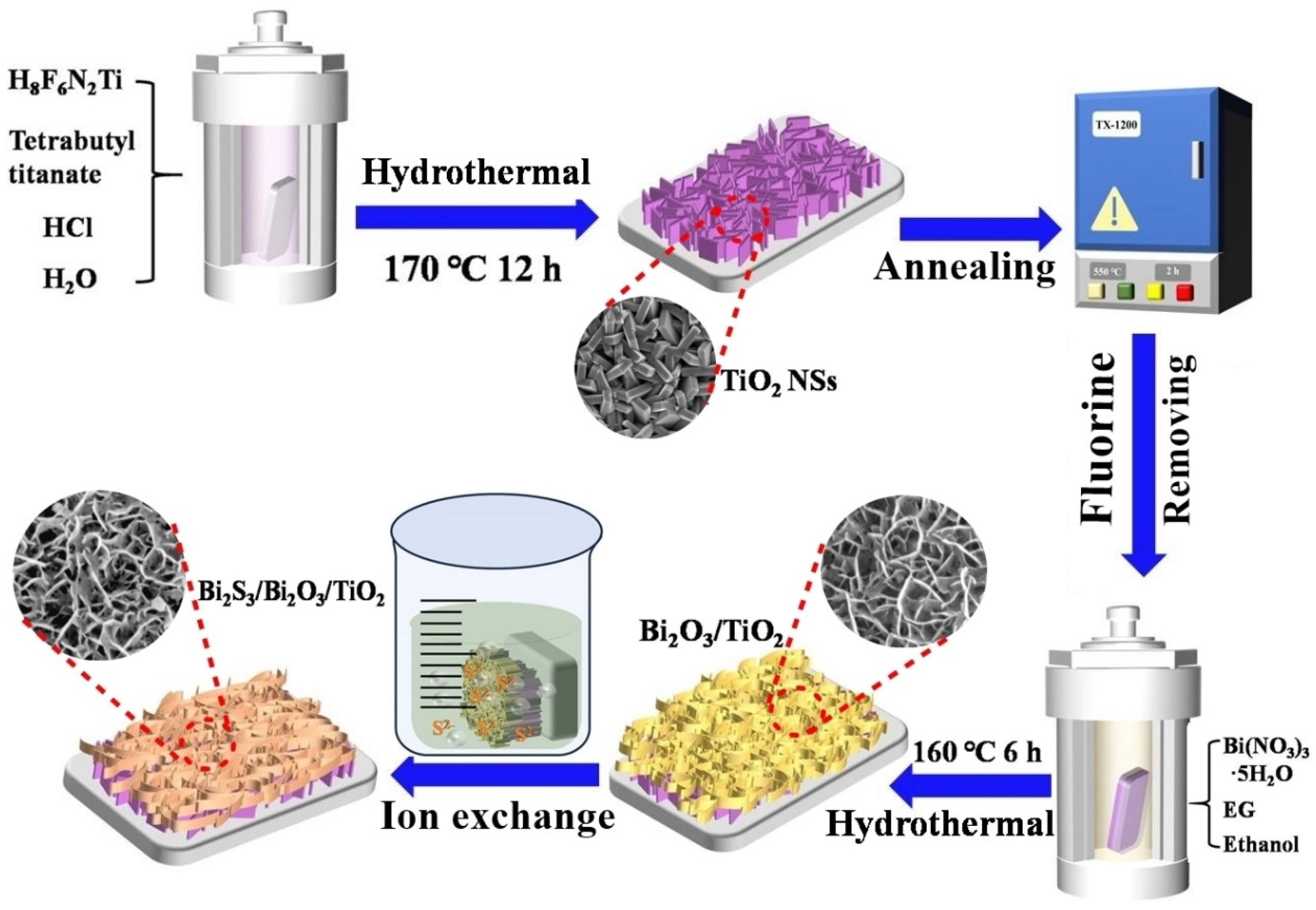
2.1. Materials

Fluoride-doped tin oxide (FTO, 2.2 mm, resistivity = 7 Ω/sq, transmittance ≥ 90%) glass substrates were purchased from Kaivo (Zhuhai, China). Acetone, isopropanol, ethanol, ethylene glycol (EG) and sodium sulfide (Na2S∙9H2O) were purchased from Sinopharm Chemical Reagent Co., Ltd. (Beijing, China). Tetrabutyl titanate (TBT), hydrochloric acid (HCl, 36~38%) and bismuth (III) nitrate pentahydrate (Bi(NO3)3∙5H2O) were purchased from Aladdin Co., Shanghai, China. Ammonium hexafluorotitanate (H8F6N2Ti) was purchased from Macklin incorporated company. All used reagents were analytical grade (AR) and without any additional purification. Aqueous solutions were prepared using ultra-pure deionized (DI) water with a resistivity of approximately 18 MΩ·cm.

2.2. Synthesis of TiO2 NSs Array Film

The TiO2 NSs array film grown on FTO substrate was fabricated by the hydrothermal method. Typically, FTO substrates with the dimensions of 1.0 × 3.0 cm2 were cleaned via sonication in acetone, isopropanol, ethanol and DI water for 20 min, respectively. The reaction precursor solution contained 30 mL of HCl/H2O (volume ratio, 1:1) and 0.8 mL of TBT. After stirring for 30 min, 0.5 g of H8F6N2Ti powder as a capping agent was added. A piece of cleaned FTO substrate was placed in a 100 mL Teflon-lined stainless-steel autoclave, followed by the addition of the homogeneous transparent solution. To synthesize TiO2 NSs film exposed to {001} facets with high reactive activity, the autoclave was transferred into a box oven and heated at 170 °C for 12 h. After cooling to atmospheric temperature naturally, the synthesized white film on FTO substrate was subjected to rinsing with DI water and then dried at 60 °C for 12 h in an oven. In the following step, the TiO2 NSs were rapidly placed into a preheated muffle furnace at 550 °C for 2 h to remove the fluorine species on the surface of TiO2 crystals.

2.3. Synthesis of Bi2S3/Bi2O3/TiO2 Dual Heterojunction Film

Firstly, the Bi2O3/TiO2 composites film was fabricated by hydrothermal method. The specific preparing process was as follows: 5 mM of Bi(NO3)3∙5H2O and 15 mL of EG were vigorously stirred to obtain a completely transparent solution. Subsequently, 30 mL of ethanol was dropped into the resultant solution. After stirring for 10 min, the mixed solution was poured into a 100 mL Teflon-lined stainless-steel autoclave. Then, FTO substrate with TiO2 NSs film was placed vertically in the autoclave. The hydrothermal fabrication procedure lasted for 6 h at the temperature of 160 °C. After the autoclave cooled to room temperature, the Bi2O3/TiO2 sample was rinsed with massive DI water and ethanol to remove other residues, and then dried at 60 °C for 12 h.
To grow Bi2S3 layer over the surface of Bi2O3/TiO2 film, in-situ anion exchange method was adopted. In a typical process, the prepared Bi2O3/TiO2 film was immersed in 0.1 M of Na2S∙9H2O solution for 5 min at room temperature. Then, the sample was taken out, thoroughly washed and dried under vacuum at 60 °C for 12 h. Figure 1 displays the schematic illustration of the synthetic process of the hierarchical heterostructure film comprising Bi2S3/Bi2O3/TiO2 on FTO substrate, achieved by a three-step method preparation process.

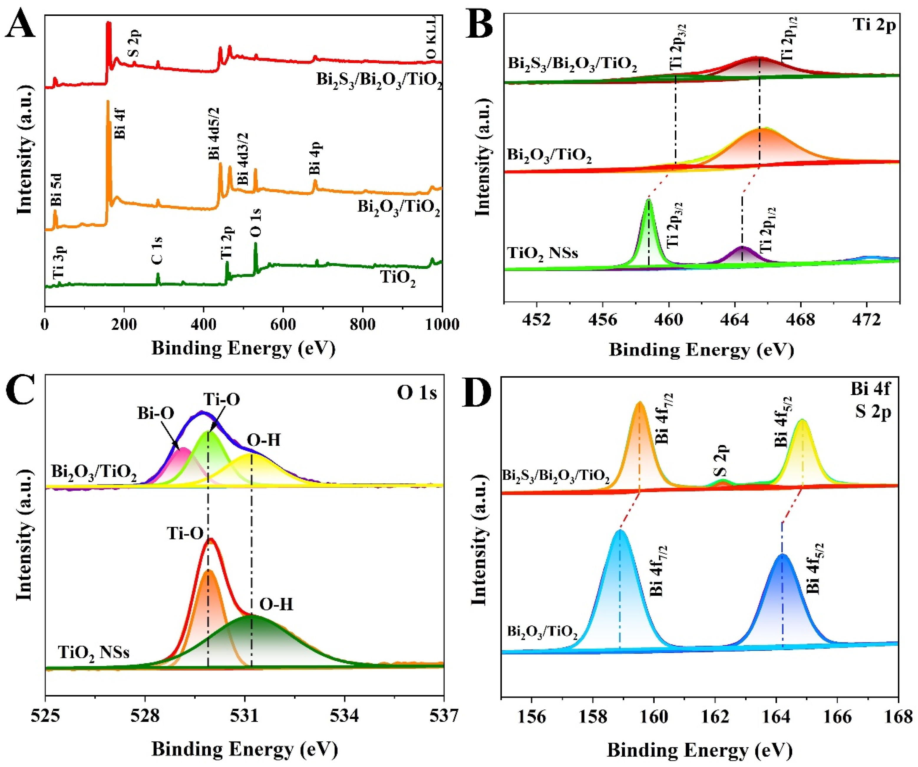
2.4. Characterization

Sample morphology was analyzed by field-emission scanning electron microscope (FESEM, MARA LMS, TESCAN). The crystal structure of as-prepared samples was performed on Rigaku D/max-2500 X-ray diffractometer using Cu Kα radiation (λ = 1.5418 Å) scanning from 20° to 80° with scanning rate of 2° min−1. The microstructure of the samples was analyzed through transmission electron microscopy (TEM, FEI, Tecnai-G2 F20) at 200 kV. Energy dispersive spectrometry (EDS) on TEM was performed for element mapping scanning. The surface chemical binding energy was determined by X-ray photoelectron spectroscopy (XPS, ESCLAB250Xi, Thermo Fisher Scientific, Waltham, MA, USA). The UV-visible (UV-vis) diffuse reflectance spectra of samples were performed on a Lambda 950 double-beam spectrophotometer to analyze the absorption property. The measurements were conducted with barium sulfate (Ba2SO4) as a reference material.

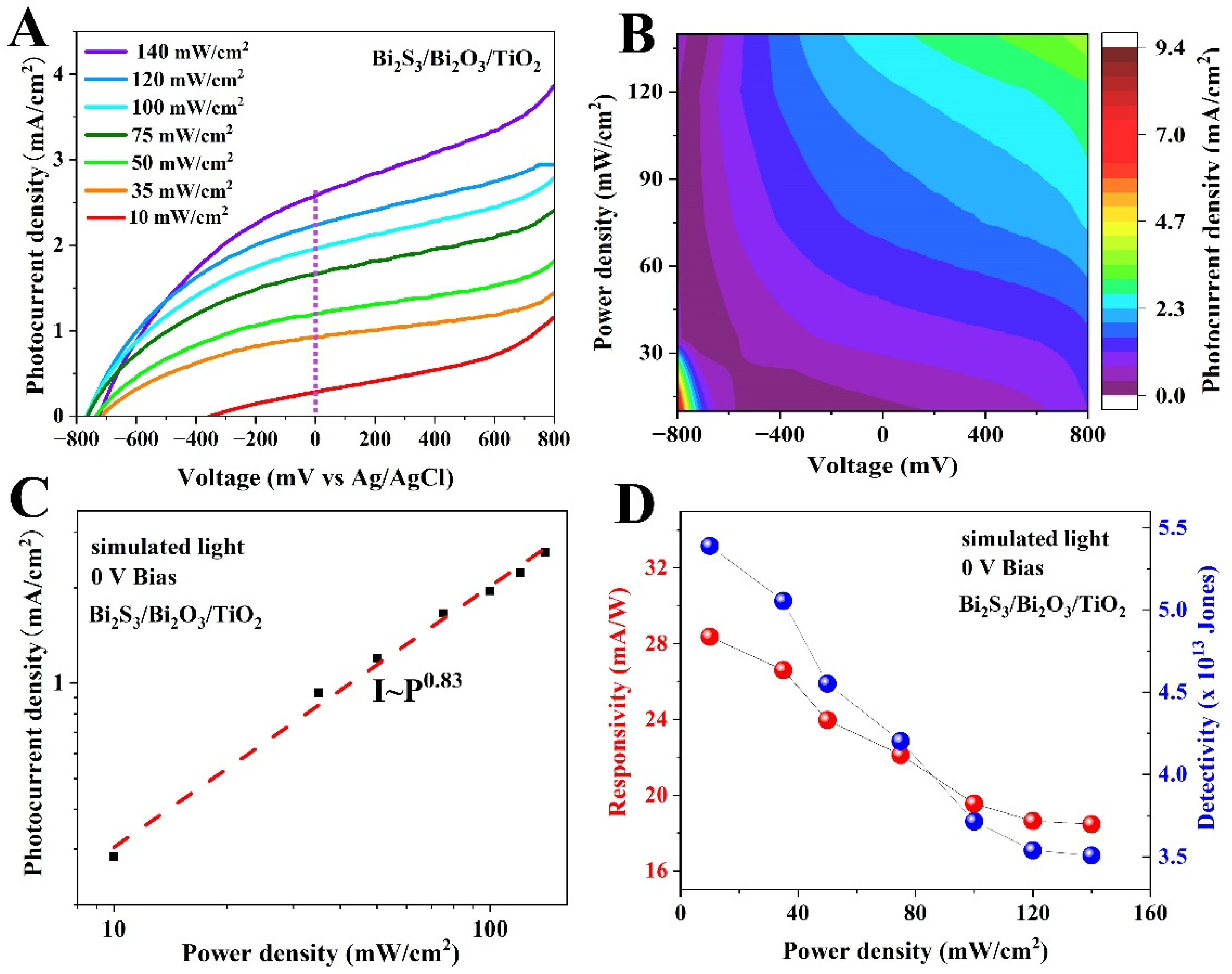
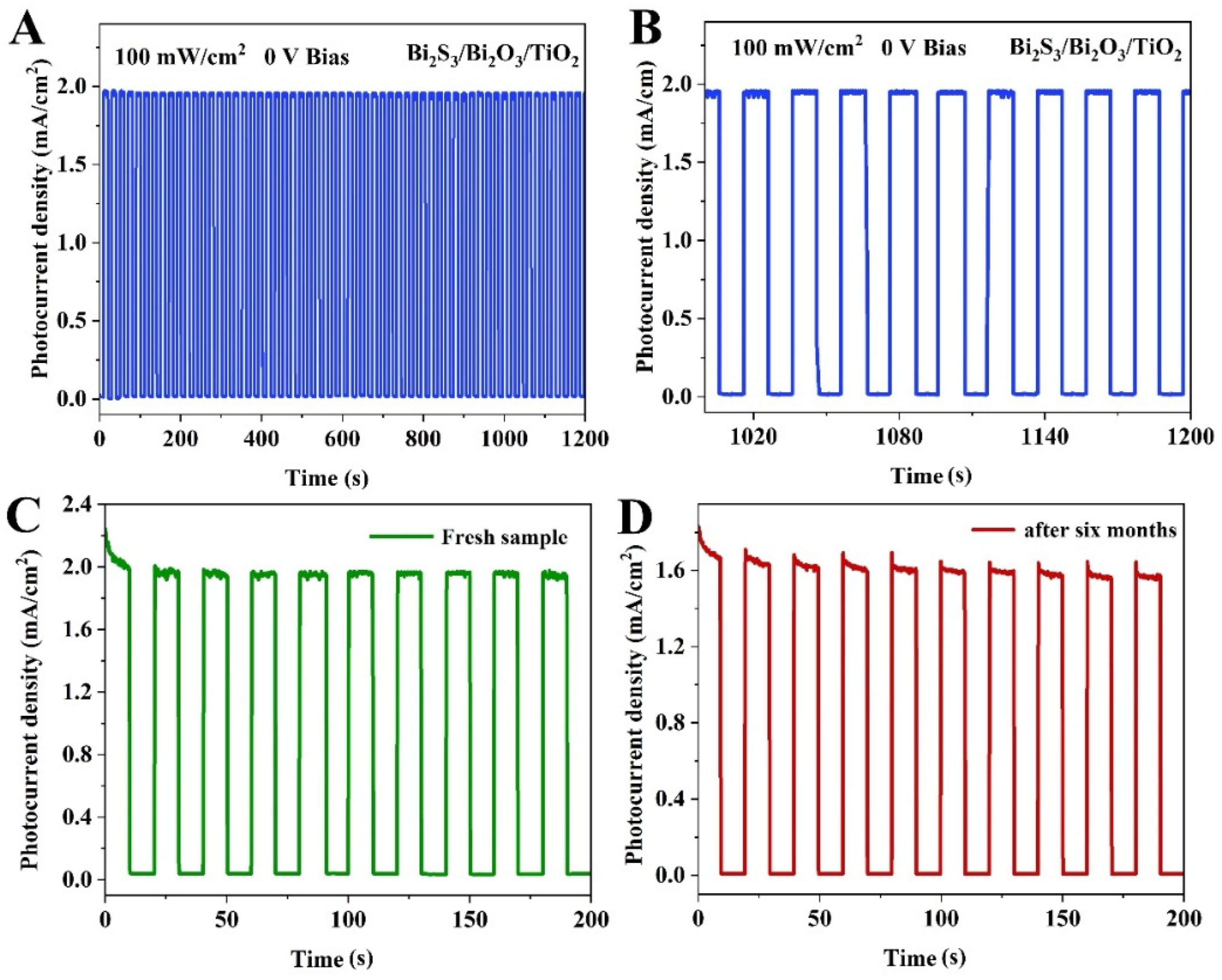
2.5. Photodetection Performance Measurements

Electrochemical workstation (CHI 660E) equipped with a three-electrode system in a quartz container was used to evaluate the PEC performance of the prepared photoelectrodes. The samples grown on FTO substrates were employed as the working photoelectrodes. Pt mesh played a role as a counter electrode, and the Ag/AgCl electrode was employed as a reference electrode, respectively. A 500 W xenon lamp was used as the simulated sunlight source. The photactive area of the working photoelectrode was maintained at 1 cm2 using a hard mask. The linear sweep voltammetry (LSV) was measured in 0.5 M KOH aqueous solution at a scan rate of 10 mV s−1. The transient photocurrent was performed by switching the light on and off. Electrochemical impedance spectroscopy (EIS) was measured at open circuit voltage with a frequency range from 0.01 to 100 kHz.

2.6. Photoelectrocatalytic Degradation of RhB

The photoelectrocatalytic activities of as-prepared pure TiO2 NSs, Bi2O3/TiO2 and Bi2S3/Bi2O3/TiO2 heterostructures were also assessed on a three-electrode system as mentioned above. The degradation process of Rhodamine B (RhB) was conducted under simulated sunlight irradiation from a 500 W xenon lamp equipped with a 420 nm cutoff filter. The characteristic absorption peak of RhB at 554 nm was used to determine the degradation ability of photoelectrodes. Typically, the work electrode was placed in 100 mL of supporting electrolyte with RhB (5 mg/L) and Na2SO4 (0.1 M) solution. Before light irradiation, the solution was magnetically stirred for 30 min in the dark to ensure an adsorption-desorption equilibrium between the RhB dye and photoelectrode. The degradation experiment was carried out at 0.8 V bias potential. 1 mL of mixed solution was taken out from the PEC reactor at 10 min intervals of illumination. After centrifugation at 8000 r/min for 5 min, the absorption behavior of the clear solution was measured by UV–vis spectrophotometer (UV-2600, Optical Instrument Factory, Shanghai, China).

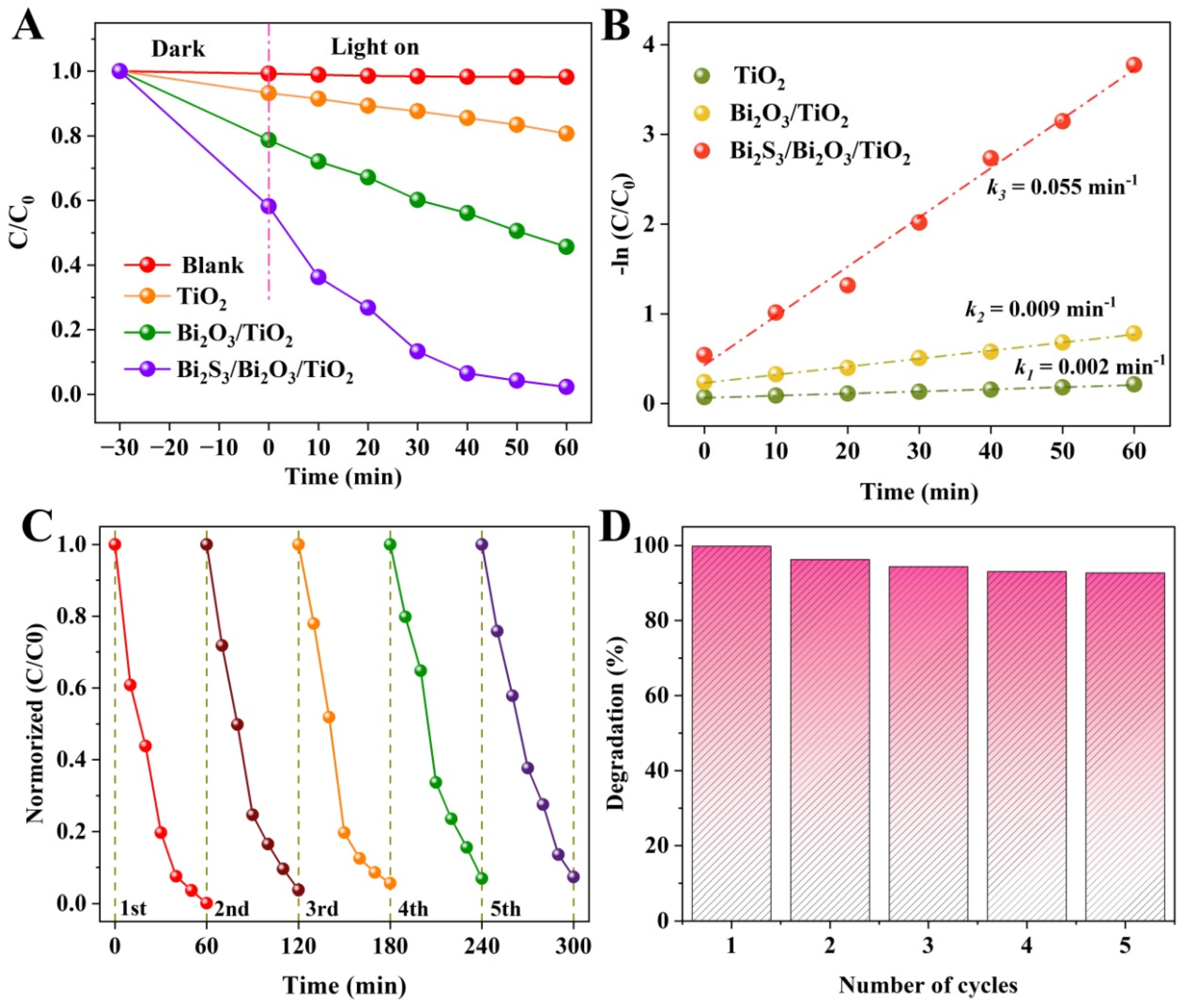
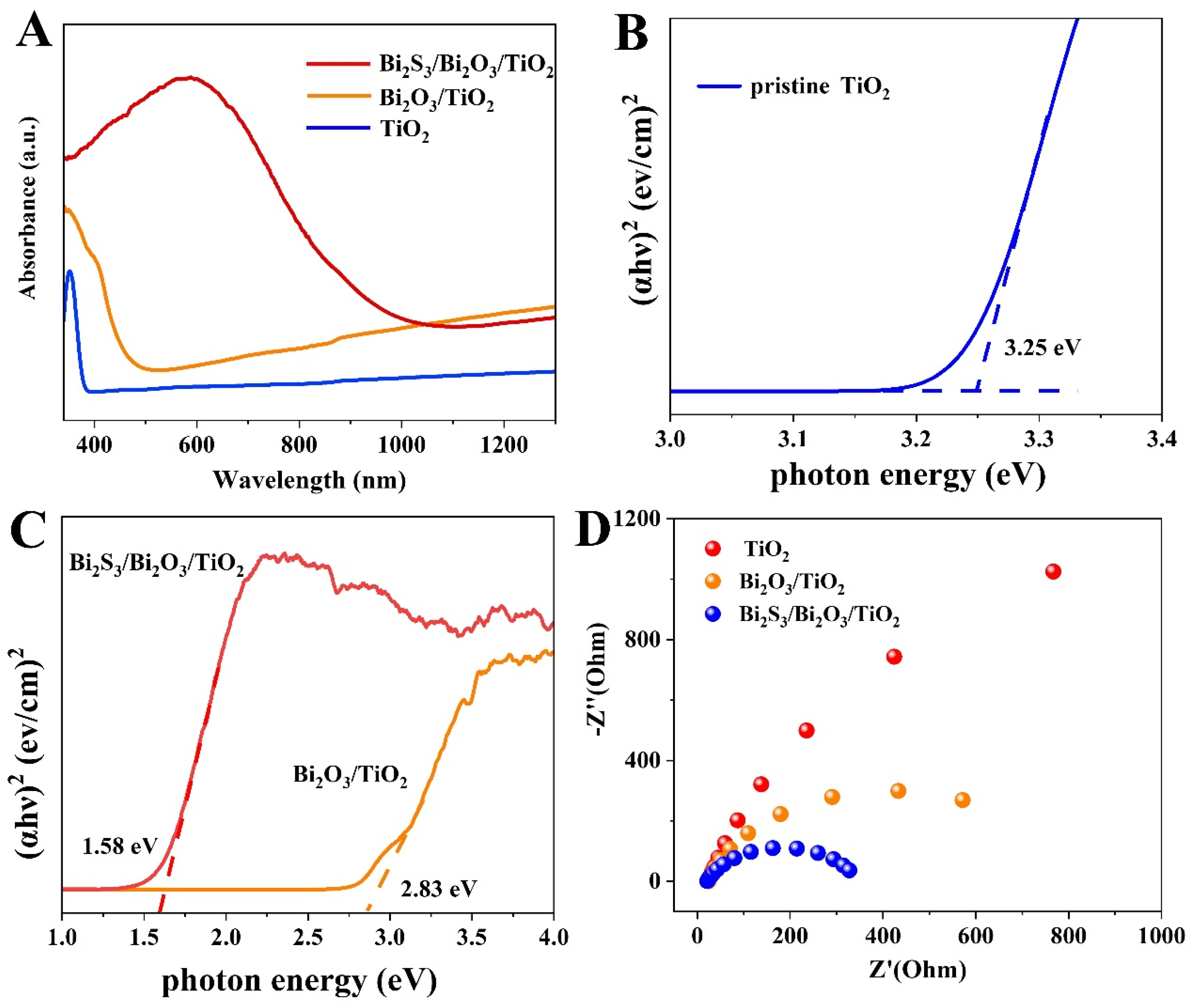
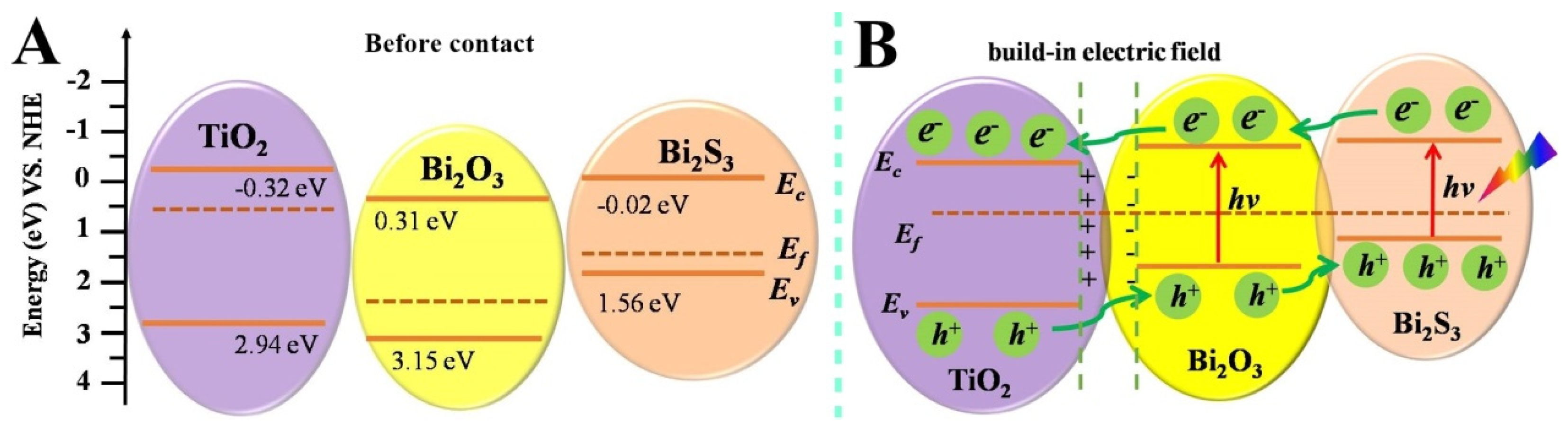
3. Results and Discussion

We developed a two-step hydrothermal and ion-exchange method to fabricate Bi2S3/Bi2O3/TiO2 hierarchical film with dual heterostructure. The morphology of the obtained samples was investigated by FESEM technology, as shown in Figure 2A–C. The phase purity and crystal texture of the obtained samples were explored by XRD patterns (displayed in Figure 2D–F). Figure 2A shows the surface characteristics of 2D TiO2 NSs array film exposed to high-energy {001} facets with high reactive activity. It can be seen that the TiO2 nanocrystals cover uniformly and grow densely on the FTO substrate. The TiO2 NSs intercross with each other to form a network with sufficient internal surface area. The thickness of TiO2 NSs is close to 230 nm. Figure 2D is the corresponding XRD diffraction peaks of pristine TiO2 NSs. It can be found that the main characteristic peaks at 25.30°, 37.77°, 48.09°, 55.18° and 62.72° belong to the (101), (004), (200), (211) and (204) crystal planes of anatase phase TiO2 (JCPDS No. 21-1272). The sharp diffraction peaks verify its high crystallinity. Furthermore, other diffraction peaks are assigned to the FTO substrate (JCPDS No. 46-1088), indicating that the sample is highly purified. For the Bi2O3/TiO2 composite film, the SEM image in Figure 2B shows that a mass of Bi2O3 nanoflakes with the thickness of ~10 nm grows on the surface of TiO2 NSs. The XRD pattern of as-prepared Bi2O3/TiO2 film is shown in Figure 2E. All diffraction peaks marked in green perfectly correspond to the standard tetragonal phase Bi2O3 (JCPDS No. 65-1209) [33]. The Bi2O3 nanoflakes grown on TiO2 NSs have a preferential growth of (101) crystallographic. After experiencing the process of anion exchange, the objective Bi2S3/Bi2O3/TiO2 heterostructure film is obtained. The surface morphology of the sample is almost similar to that of Bi2O3/TiO2 film, as shown in Figure 2C. However, the space existing between the nanoflakes is distinctly enlarged, contributing to the corrosive effect on Bi2O3 nanoflakes in the anion-exchange process [34]. Meanwhile, it can be seen that the crystal phase structure of Bi2O3 nanoflakes is also transformed to monoclinic phase Bi2O3 (JCPDS No. 41-1449) after surface sulphuration, as shown in Figure 2F. Noticeably, it is also observed that new and obvious characteristic peaks (marked in purple) appear, which are matched to the orthorhombic phase Bi2S3 (JCPDS No. 3-0362). The main diffraction peaks located at 29.17° and 46.91° match well with the (320) and (501) planes of Bi2S3, respectively. The features strongly illustrate that the Bi2S3/Bi2O3/TiO2 heterojunction film has been successfully obtained.
The detailed microstructures of pristine TiO2, Bi2O3/TiO2 and Bi2S3/Bi2O3/TiO2 films were further investigated by TEM and high-resolution TEM (HRTEM). TEM image in Figure 3A shows a tetragonal structure of a pristine TiO2 sample. After the growth of Bi2O3 and Bi2S3 layers, TiO2 NSs building units can also be easily identified, as shown in Figure 3B,C. The results suggest that the preparation process of Bi2O3 and Bi2S3 layers did not destroy the structure of TiO2 NSs. HRTEM image of pristine TiO2 is shown in Figure 3D. The measured lattice spacing of 0.35 nm (shown in the inset) is indexed to (101) atomic planes of anatase phase TiO2. The clear stripes verify its good crystalline. In addition, the fast Fourier transform (FFT) array pattern shown in the inset of Figure 3D suggests the monocrystalline characteristics of TiO2 NSs and can be indexed as [001] zone axis diffraction, which indicates that the square surfaces are high-reactive {001} facets. Figure 3B,E show the TEM and HRTEM images of Bi2O3/TiO2 sample, respectively. The surface of the sample becomes rough, as shown in Figure 3B. It is noticeable that besides the stripes from TiO2 (101) plane (marked in red in Figure 3E), the lattice fringes with d-spacing of 0.18 nm correspond to the (401) planes of Bi2O3, which provides the direct strong evidence of the formation of Bi2O3/TiO2 heterostructure. Figure 3C,F show TEM and HRTEM images of Bi2S3/Bi2O3/TiO2. The lattice spacings of 0.19 nm and 0.30 nm are indexed to the (203) plane of Bi2O3 layer and (320) plane of Bi2S3 layer, respectively. Figure 3G shows TEM-EDS mapping patterns of the Bi2S3/Bi2O3/TiO2 sample. The images clearly show the uniform distribution of Ti, O, Bi and S elements in the sample. The Ti element is mainly distributed in the core region, while O, Bi and S elements cover the entire region. The results confirm that Bi2S3 layer is interlaced in the Bi2O3 nanoflakes matrix and forms an interface heterostructure in Bi2S3/Bi2O3/TiO2 film.
The surface elemental configuration and chemical valence states of as-prepared TiO2, Bi2O3/TiO2 and Bi2S3/Bi2O3/TiO2 films were determined by XPS measurements. The binding energy of C 1s (at approximately 284.6 eV) was used to calibrate the XPS spectra from other elements. The C element comes from the carbon-based contaminant on the surface of samples [35]. Based on the survey spectra in Figure 4A, it can be observed that the Bi2S3/Bi2O3/TiO2 film is composed of Ti, O, Bi and S elements, coinciding with the analysis of EDS element mapping images displayed above. In the Ti 2p high-resolution scan spectrum of anatase TiO2 film (Figure 4B), the peaks at 458.78 and 464.65 eV are assigned to Ti4+ 2p3/2 and Ti4+ 2p1/2 energy levels, respectively. By contrast, the Ti 2p characteristic peaks in Bi2O3/TiO2 film shift to 460.48 and 465.30 eV. The shift is ascribed to the strong interaction between Bi2O3 nanoflakes and TiO2 NSs [36]. Furthermore, the characteristic peaks of Ti 2p of Bi2S3/Bi2O3/TiO2 are almost in line with that of Bi2O3/TiO2, suggesting that surface sulphuration by anion exchange method has little effect on the environment around Ti atom. O 1s spectra from pristine TiO2 and Bi2O3/TiO2 are shown in Figure 4C. Figure S1 (Supporting Information) shows that of Bi2S3/Bi2O3/TiO2 film. The O 1s spectrum of TiO2 film contains two peaks at 529.92 and 531.20 eV, corresponding to Ti–O bond and absorbed surface hydroxyl groups [37], respectively. It can be obviously observed that a new characteristic peak appears at approximately 529.15 eV in Bi2O3/TiO2 and Bi2S3/Bi2O3/TiO2 film, assigning to Bi–O bond. The results demonstrate the existence of Bi2O3 layer in composites film. The Bi 4f spectra of Bi2O3/TiO2 and Bi2S3/Bi2O3/TiO2 composites are shown in Figure 4D. There are two symmetrical peaks at 158.89 (Bi3+ 4f7/2) and 164.21 eV (Bi3+ 4f5/2) for Bi2O3/TiO2 film. While they move slightly to higher binding energy in Bi2S3/Bi2O3/TiO2 film, verifying interfacial charges transfer between Bi2S3 and Bi2O3 layer. The weak peak (at approximately 162.26 eV) between Bi 4f7/2 and Bi 4f5/2 of Bi2S3/Bi2O3/TiO2 is assigned to S 2p binding energy. In addition, the characteristic peak referred to S 2s (as shown in Figure S1, Supporting Information) can also be found in Bi2S3/Bi2O3/TiO2 film. The peak positioned at 225.4 eV is referred to Bi–S bond, functioning as a fast electron bridge for interface carrier transport. The peak located at 228.2 eV matches well with the S8 species [38]. The results further confirm the existence of Bi2S3 and Bi2O3 in the composite film.
To evaluate the potential photodetection application, a three-electrode system was constructed and the PEC performance of the devices based on TiO2, Bi2O3/TiO2 and Bi2S3/Bi2O3/TiO2 photoelectrode films was measured on an electrochemical workstation, as shown in Figure 5A. The LSV curves in 0.5 M KOH electrolyte under darkness are shown in Figure S2 (Supporting Information). The dark current (Idark) of Bi2S3/Bi2O3/TiO2 device is approximately 1.9 × 10⁻⁶ mA cm−2 at 0 V bias, an order of magnitude lower than those of TiO2 (6.8 × 10⁻⁵ mA cm−2) and Bi2O3/TiO2 (1.6 × 10⁻⁵ mA cm−2) devices. The phenomenon verifies a low leakage current in Bi2S3/Bi2O3/TiO2 device, which is attributed to the dual heterostructure formation and the reduced charge carrier recombination rate. Figure 5B shows the LSV curves of PEC devices under simulated sunlight illumination at 100 mW cm−2. All of the PEC devices display obvious photosensitivity to sunlight. The photocurrent density (Ilight) is almost stable within the test range, indicating the photoelectrodes do not experience electrochemical corrosion. In addition, the photocurrent of all three PEC devices shows obvious dependence on external bias potential. As shown in Figure S3 (Supporting Information), it can be found that the photocurrent of Bi2S3/Bi2O3/TiO2 device is always larger than those of the other devices at various bias potentials, which increases from 1.95 mA cm−2 at 0 V to 2.79 mA cm−2 at 0.8 V with an improvement of 43%. The sensitive characteristic to external bias potential gives flexibility to regulate photodetection performance in the actual usage scenario. The photoresponsivity (R) and photodetectivity (D*) are significant parameters to assess quantitatively the photoresponse performance of PEC photodetectors, which can be calculated using the following formulas [39,40]:
R = I l i g h t I d a r k P i n S
D * = R S 1 / 2 ( 2 e I d a r k ) 1 / 2
where Ilight is the photocurrent density under illumination, Idark is the current recorded in dark condition, Pin is the incident light power intensity, S is the effective area of the device and e is the elementary charge with a value of 1.60 × 10⁻¹⁹ C, respectively. Particularly, it can be found from Figure 5C,D that R and D* of the PEC devices display a gradual rising trend with an increasing bias potential. The phenomenon is attributing that separation and transport of photogenerated carriers can be efficiently promoted by the effect of external potential. As for the Bi2S3/Bi2O3/TiO2 device, the optimal R and D* reach up to 27.9 mA W−1 and 5.7 × 10¹³ Jones at 0.8 V, respectively. By contrast, the Bi2S3/Bi2O3/TiO2 device presents the best photoelectric performance, suggesting its more excellent ability of rapid charge carrier separation and transport.
Figure 5E shows the transient photocurrent density of various PEC devices at 0 V bias under periodic illumination at 10 s intervals. Impressively, the photocurrent density rapidly increases upon illumination and instantly decreases without light, indicating an obvious switching behavior. The photoresponse performance remains stable after several cycling tests, exhibiting their huge potential in self-powered device applications [41]. The light on/off ratio (Ilight/Idark) is another critical indicator to evaluate the performance of photodetectors. The calculated on/off ratio of PEC device based on Bi2S3/Bi2O3/TiO2 film is approximately 1.3 × 10⁶, higher that of Bi2O3/TiO2 (4.3 × 10⁴) and TiO2 (1.5 × 10³) devices, demonstrating Bi2S3/Bi2O3/TiO2 heterostructure composite film achieves superior photoelectrical performance. Moreover, the response and recovery characteristics were investigated to judge the response speed to external illumination, as shown in Figure 5F and Figure S4 (Supporting Information). The rise time (tr) is defined as the time interval for the photocurrent to increase from 10% to 90% of the saturated photocurrent, and the decay time (td) refers to the time interval for the photocurrent to recover from 90% to 10% of the saturated photocurrent. The rise and decay times of Bi2S3/Bi2O3/TiO2 device are 63 ms and 95 ms, significantly superior to those of Bi2O3/TiO2 and TiO2 devices, as shown in Figure 5G. The results verify the high photoresponse speed of the Bi2S3/Bi2O3/TiO2 PEC device.
The photoresponse behaviors of Bi2S3/Bi2O3/TiO2 photodetector with various light power intensities were investigated. Figure 6A shows LSV curves of Bi2S3/Bi2O3/TiO2 PEC devices under different light power densities. It can be observed that the photocurrent gradually enhances as the bias potential increase with constant light intensity. Figure 6B displays a photocurrent density map as a function of both applied potential and light power density. It can be found that the photocurrent density also increases along with light power intensity, demonstrating a stable detecting ability. Specifically, the photocurrent at 0 V bias steadily increases from 0.28 to 2.58 mA cm−2 as the power intensity increases from 10 to 140 mW cm−2, resulting from more photogenerated charge in photoelectrode film at high light power intensity. As known, the dependence of the photocurrent (I) on the light power intensity (P) can be well fitted by the power law I~Pθ. The exponent θ is determined by the photocurrent response to light intensity [42]. The θ value in the curve of Bi2S3/Bi2O3/TiO2 film shown in Figure 6C is determined as approximately 0.83. The linear dependence between the photocurrent density and the incident power indicates that there is an extremely low trap state density or an acceleration of detrapping dynamics with increasing carrier density. The calculated R and D* dependent on light power intensity is displayed in Figure 6D. With the increasing light power intensity, the values of R and D* present a downward trend and become saturated, which is attributed to the serious scattering or recombination rate of photogenerated carriers in higher incident power conditions [43,44]. When light power intensity is 100 mW cm−2, R and D* for the Bi2S3/Bi2O3/TiO2 film are approximately 19.6 mA W−1 and 3.7 × 10¹³ Jones at 0 V, respectively. The stability of the PEC photodetector is vital for the commercial practical application. Figure 7A shows the long-term stability of the Bi2S3/Bi2O3/TiO2 PEC device at the bias voltage of 0 V. Under the light intensity of 100 mW cm−2 for 1200 s, the photocurrent exhibits a negligible photocurrent density deficiency, demonstrating the excellent sustainability of the PEC device. Additionally, the storage stability of the device in air for six months is investigated, as shown in Figure 7C,D. After storage in air environment for six months, the photocurrent decreased to 1.56 mA cm−2, which may result from adsorbed humidity, oxygen or contamination from environment. The results suggest that the device has ultrahigh stability and huge application prospect. Moreover, a comparison of the performance metrics of Bi2S3/Bi2O3/TiO2 photodetectors has been summarized in Table 1. It can be found that the designed Bi2S3/Bi2O3/TiO2 PEC photodetector appears to have comparable photoresponsivity and response time. Noticeably, the detectivity of Bi2S3/Bi2O3/TiO2 PEC photodetector is superior to other reference devices.
The photoelectrocatalytic activities of samples were evaluated by the degradation of RhB contaminant at 0.8 V bias. Figure 8A displays the degradation curves of the RhB contaminant with irradiation time over different photoelectrocatalysts. The blank test verifies that RhB dye is scarcely degraded by photolysis without photoelectocatalyst. The pristine TiO2 NSs film exhibits a weak photoelectrocatalytic activity and only degraded 20% of RhB in 60 min. While the RhB removal efficiency is boosted to 55% in the presence of Bi2O3/TiO2 photoelectrode, indicating that the formation of heterostructure is beneficial to improve photoelectrocatalytic performance. For Bi2S3/Bi2O3/TiO2 composites with dual heterojunctions, degrading efficiency rapidly reaches up to 75% after 20 min illumination. It is worth noting that the RhB dye is almost completely degraded within 60 min. The corresponding reaction kinetics of RhB degradation is shown in Figure 8B. All degradation experiments under illumination are found to follow the pseudo-first-order decay kinetics. The kinetics constants of TiO2, Bi2O3/TiO2 and Bi2S3/Bi2O3/TiO2 are 0.055, 0.009 and 0.002 min−1 for 0.8 V bias potential, respectively. The results indicate that the Bi2S3/Bi2O3/TiO2 composites achieve optimal photoelectrocatalytic degradation activity, suggesting the recombination of photogenerated electrons and holes is further suppressed. In addition, the self-supported Bi2S3/Bi2O3/TiO2 photoelectrocatalysts on the FTO substrate are recyclable and reusable. After five cycling runs (shown in Figure 8C,D), the RhB degradation efficiency still remained at 92%, demonstrating the good stability of the photoelectrode.
In our present work, the obtained Bi2S3/Bi2O3/TiO2 photoelectrode film reveals enhanced PEC performance compared with pure TiO2, and Bi2O3/TiO2 composites. The excellent PEC activity is attributed to the nature of Bi2S3 and Bi2O3 semiconductors. Figure 9A presents the UV-vis absorbance spectra of prepared samples. It can be found that pristine TiO2 film only exhibits an evident response to the ultraviolet light region due to its band gap of approximately 3.25 eV (shown in Figure 9B), similar to the previous report [26]. After being composited with Bi2O3 nanoflakes, the absorption range is broadened to approximately 500 nm. From the Tauc plot of Bi2O3/TiO2 displayed in Figure 9C, the band gap of Bi2O3 can be determined as approximately 2.83 eV, a similar value to that reported in the literature [26]. In contrast, the Bi2S3/Bi2O3/TiO2 composites film shows an obvious absorption between 400 and 900 nm, resulting from the coupled Bi2S3 layer on the surface with a band gap of approximately 1.58 V, close to the value in the previous report [31]. Moreover, the stronger absorption is found for the Bi2S3/Bi2O3/TiO2 film, which may be ascribed to the design of the hierarchical configuration in favor of light refraction and harvesting. As a result, the composite film can readily utilize low-energy photons and generate more charge carriers to improve the PEC performance. Electrochemical impedance spectroscopy (EIS) has been measured in order to investigate the transport behavior of charge carriers, as shown in Figure 9D. The radius is closely related to the charge transfer process at the photoelectrode-electrolyte interface. It is found that the Bi2S3/Bi2O3/TiO2 exhibits the smallest charge transfer resistance, benefitting from the migration of charge carriers. Therefore, the excellent charge-transfer capacity of Bi2S3/Bi2O3/TiO2 also contributes to the enhancement of photoresponse and photoelectrocatalysis performance.
To further explain the possible enhanced mechanism of PEC performance, the energy band structure in the Bi2S3/Bi2O3/TiO2 composite film is investigated in detail. The energy band alignment between Bi2S3, Bi2O3 and TiO2 plays a significant role in separating the photogenerated electron and hole pair. The specific conduction band (CB) and valence band (VB) edge potentials of the three semiconductors can be predicted by the following empirical equations [50]:
E CB   =   X       E 0     0.5 E g
E VB = X     E 0 + 0.5 E g
where X is the absolute electronegativity of the semiconductor, E0 is the energy of free electrons on the hydrogen scale (~4.5 eV), and Eg is the band gap of the semiconductor. The X values for TiO2, Bi2O3 and Bi2S3 are 5.81, 6.23 and 5.27 eV, respectively. Based on the formulas mentioned above, the calculated values of ECB, EVB for TiO2, Bi2O3 and Bi2S3 semiconductors are listed in Table S1 (Supporting Information). On the basis of the relevant values, the energy band structure of the TiO2, Bi2O3 and Bi2S3 before contact is shown in Figure 10A. Commonly, TiO2 is considered as an intrinsic n-type semiconductor [51], its Fermi energy level approaches to the conduction band. While Bi2O3 and Bi2S3 are considered as p-type semiconductors, so the Fermi level is close to the valence band. After the semiconductors are closely connected together, the Fermi level in TiO2 NSs shift downward and those in Bi2O3 and Bi2S3 rise, until they reach a thermal equilibrium Fermi level [26]. Meanwhile, their valence and conduction bands undergo realignment and form a built-in electric field. The descended conduction band and ascended valence band indicate that type-II type heterojunction is established in the Bi2S3/Bi2O3/TiO2 composite film, as shown in Figure 10B. Under illumination, Bi2O3 and Bi2S3 with a relatively narrow band gap are excited to produce charge carriers. The photogenerated electrons on the conduction band of the p-type Bi2S3 and Bi2O3 transfer to that of n-type TiO2, whereas the in the valence band of TiO2 are transferred to the valence band of Bi2O3 and Bi2S3 under the effect of the built-in electric field. As discussed above, the p-n heterojunction inhibits the recombination of photogenerated charge carriers, which contributes to more photogenerated carriers participating in PEC reactions for photodetection and photoelectrocatalysis. Specifically, holes accumulated on the surface of Bi2S3 layer oxidize OH anions in the electrolytes to form OH*, as shown in Figure S5 (Supporting Information). Electrons accumulated on the surface of TiO2 swiftly move to the FTO conductive substrate and transport to the counter electrode (Pt) through the external circuit. At the solid-liquid interface, the photogenerated electrons reduce the radical OH* to form OH anions. The movement of photogenerated electrons generates the electric signal, which can realize the function of photodetection. In the photoelectrocatalystic degradation process, electrons are captured by oxygen adsorbed on the surface of Pt electrode to generate O2. Meanwhile, the holes gather at the photoelectrode/electrolyte interface and can directly oxidize the RhB dye or cause indirect oxidation through the generation of oxidizing species such as the hydroxyl radical. According to the above analysis, the enhanced PEC performance of Bi2S3/Bi2O3/TiO2 film is mainly due to the formation of dual heterostructures and the broadband light response.

4. Conclusions

In summary, we have demonstrated a two-step hydrothermal method to synthesize hierarchical Bi2O3/TiO2 heterojunction film. After in-situ surface sulphuration, the Bi2S3 layer was successfully incorporated onto the surface of Bi2O3/TiO2 composites, forming dual heterojunctions that promote both charge migration and light harvesting with the reduced recombination of charge carriers. The composite film exhibits excellent PEC activity with high stability under illumination, which is much higher than that of pure TiO2 and Bi2O3/TiO2 composites. The light on/off current ratio of Bi2S3/Bi2O3/TiO2 device approximately reaches to 1.3 × 10⁶ at 0 V bias. Furthermore, the photoelectrode film demonstrated approximately 97.7% degradation after 60 min of PEC reaction. This comprehensive investigation enhances our understanding of developing high-performance optoelectronic devices and paves the way for advancements in multifunctional PEC devices.

Supplementary Materials

The following supporting information can be downloaded at: https://www.mdpi.com/article/10.3390/ma18153528/s1, Figure S1: High-resolution XPS spectra of O 1s and S 2s in Bi2S3/Bi2O3/TiO2 film. Figure S2: LSV curves under dark. Figure S3: Histogram of photocurrent density at various bias potential for different PEC devices. Figure S4: Transient photocurrent at 0 V bias of (A) pristine TiO2 and Bi2O3/TiO2 film. Table S1: Calculated ECB and EVB of TiO2, Bi2O3 and Bi2S3. Figure S5: Schematic illustration of PEC photodetector based on Bi2S3/Bi2O3/TiO2 composites film.

Author Contributions

Conceptualization, L.L.; methodology, L.L.; validation, L.L. and H.Y.; investigation, L.L.; data curation, L.L.; writing—original draft preparation, L.L.; writing—review and editing, H.Y.; project administration, H.Y.; funding acquisition, H.Y. All authors have read and agreed to the published version of the manuscript.

Funding

This work was supported by the National Natural Science Foundation of China (Grant No. 12004257), the National Key Research and Development Program of China (Grant No. 2023YFB3208500), the Key Research and Development Program of Shanxi Province (Grant No. 202302030201001), the Fundamental Research Program of Shanxi Province (Grant No. 202303021221117 and 202403021212341), and the Postdoctoral Fellowship Program of CPSF (Grant No. GZC20241576).

Institutional Review Board Statement

Not applicable.

Informed Consent Statement

Not applicable.

Data Availability Statement

The original contributions presented in this study are included in the article/Supplementary Material. Further inquiries can be directed to the corresponding author.

Conflicts of Interest

The authors declare no conflict of interest.

References

  1. Lianos, P. Review of recent trends in photoelectrocatalytic conversion of solar energy to electricity and hydrogen. Appl. Catal. B Environ. 2017, 210, 235–254. [Google Scholar] [CrossRef]
  2. Xu, Y.; Wang, F.; Lei, S.; Wei, Y.; Zhao, D.; Gao, Y.; Ma, X.; Li, S.; Chang, S.; Wang, M.; et al. In situ grown two-dimensional TiO2/Ti3CN MXene heterojunction rich in Ti3+ species for highly efficient photoelectrocatalytic CO2 reduction. Chem. Eng. J. 2023, 452, 139392. [Google Scholar] [CrossRef]
  3. Sorokina, L.; Savitskiy, A.; Shtyka, O.; Maniecki, T.; Szynkowska-Jozwik, M.; Trifonov, A.; Pershina, E.; Mikhaylov, I.; Dubkov, S.; Gromov, D. Formation of Cu-Rh alloy nanoislands on TiO2 for photoreduction of carbon dioxide. J. Alloys Compd. 2022, 904, 164012. [Google Scholar] [CrossRef]
  4. Wang, W.; Liu, X.; Jing, J.; Mu, J.; Wang, R.; Du, C.; Su, Y. Photoelectrocatalytic peroxymonosulfate activation over CoFe2O4-BiVO4 photoanode for environmental purification: Unveiling of multi-active sites, interfacial engineering and degradation pathways. J. Colloid Interface Sci. 2023, 644, 519–532. [Google Scholar] [CrossRef]
  5. Xiong, Y.; Ma, S.; Hong, X.; Long, J.; Wang, G. Photoelectrocatalytic Processes of TiO2 Film: The Dominating Factors for the Degradation of Methyl Orange and the Understanding of Mechanism. Molecules 2023, 28, 7967. [Google Scholar] [CrossRef] [PubMed]
  6. García-Ramírez, P.; Pineda-Arellano, C.A.; Millán-Ocampo, D.E.; Álvarez-Gallegos, A.; Sirés, I.; Silva-Martínez, S. Photoelectrocatalytic chemical oxygen demand analysis using a TiO2 nanotube array photoanode. Electrochim. Acta 2024, 476, 143710. [Google Scholar] [CrossRef]
  7. Liu, X.; Wang, D.; Shao, P.; Sun, H.; Fang, S.; Kang, Y.; Liang, K.; Jia, H.; Luo, Y.; Xue, J.; et al. Achieving record high external quantum efficiency >86.7% in solar-blind photoelectrochemical photodetection. Adv. Funct. Mater. 2022, 32, 2201604. [Google Scholar] [CrossRef]
  8. Zhou, S.; Jiang, C.; Han, J.; Mu, Y.; Gong, J.R.; Zhang, J. High-Performance self-powered PEC photodetectors based on 2D BiVO4/MXene Schottky Junction. Adv. Funct. Mater. 2025, 35, 2416922. [Google Scholar] [CrossRef]
  9. Ma, Y.; Huang, Y.; Huang, J.; Xu, Z.; Yang, Y.; Xie, C.; Zhang, B.; Ao, G.; Fu, Z.; Li, A.; et al. Optimizing Photoelectrochemical UV Imaging Photodetection: Construction of Anatase/Rutile Heterophase Homojunctions and Oxygen Vacancies Engineering in MOF-Derived TiO2. Molecules 2024, 29, 3096. [Google Scholar] [CrossRef]
  10. Shu, J.; Tang, D. Recent advances in photoelectrochemical sensing: From engineered photoactive materials to sensing devices and detection modes. Anal. Chem. 2020, 92, 363–377. [Google Scholar] [CrossRef]
  11. Leng, W.H.; Zhang, Z.; Zhang, J.Q.; Cao, C.N. Investigation of the kinetics of a TiO2 photoelectrocatalytic reaction involving charge transfer and recombination through surface states by electrochemical impedance spectroscopy. J. Phys. Chem. B 2005, 109, 15008–15023. [Google Scholar] [CrossRef]
  12. Sun, C.; Wu, L.; Hu, J.; Hussain, S.A.; Yang, J.; Jiao, F. A novel dual S-scheme heterojunction photocatalyst β-Bi2O3/NiAl-LDH/α-Bi2O3 induced by phase-transformed bismuth oxide for efficient degradation of antibiotics in full-spectrum: Degradation pathway, DFT calculation and mechanism insight. Chem. Eng. J. 2023, 474, 145616. [Google Scholar] [CrossRef]
  13. Shanmugapriya, V.; Arunpandiyan, S.; Hariharan, G.; Bharathi, S.; Selvakumar, B.; Arivarasan, A. Enhanced electrochemical performance of mixed metal oxide (Bi2O3/ZnO) loaded multiwalled carbon nanotube for high-performance asymmetric supercapacitors. J. Energy Storage 2022, 55, 105739. [Google Scholar] [CrossRef]
  14. Feng, X.; Zou, H.; Zheng, R.; Wei, W.; Wang, R.; Zou, W.; Lim, G.; Hong, J.; Duan, L.; Chen, H. Bi2O3/BiO2 nanoheterojunction for highly efficient electrocatalytic CO2 reduction to formate. Nano Lett. 2022, 22, 1656–1664. [Google Scholar] [CrossRef]
  15. Zhang, J.; Xiong, Z.; Wang, Z.; Sun, J. Study on the Preparation and PEC-Type Photodetection Performance of β-Bi2O3 Thin Films. Materials 2024, 17, 3779. [Google Scholar] [CrossRef] [PubMed]
  16. Liu, X.; Sun, Z.; Sun, Y.; Lin, H.; Chen, Z.; Chen, X.; Niu, L.; Zhang, Q.; Li, H. Fast and Long-Lasting Potassium-Ion Storage Enabled by Rationally Engineering Strain-Relaxation Bi/Bi2O3 Nanodots Embedded in Carbon Sheets. Adv. Funct. Mater. 2023, 33, 2307205. [Google Scholar] [CrossRef]
  17. Praveen, S.; Veeralingam, S.; Badhulika, S. A Flexible Self-Powered UV Photodetector and Optical UV Filter Based on β-Bi2O3/SnO2 Quantum Dots Schottky Heterojunction. Adv. Mater. Interfaces 2021, 8, 2100373. [Google Scholar] [CrossRef]
  18. Yang, S.; Jiao, S.; Nie, Y.; Lu, H.; Liu, S.; Zhao, Y.; Gao, S.; Wang, D.; Wang, J.; Li, Y. A self-powered high performance UV-Vis-NIR broadband photodetector based on β-Bi2O3 nanoparticles through defect engineering. J. Mater. Chem. C 2022, 10, 8364–8372. [Google Scholar] [CrossRef]
  19. Guo, P.; Yin, F.; Zhang, J.; Chen, B.; Ni, Z.; Shi, L.; Han, M.; Wu, Z.; Li, G. Crystal-Phase and Surface-Structure Engineering of Bi2O3 for Enhanced Electrochemical N2 Fixation to NH3. ACS Appl. Mater. Interfaces 2024, 16, 17540–17552. [Google Scholar] [CrossRef]
  20. Liu, Y.; Chu, C.; Li, Y.; Deng, P.; Liu, Y.; Wu, R.; Liu, X.; Zheng, Y.; Zhang, W.; Wu, J.; et al. Enhanced supercapacitor performance of Bi2O3 by Mn doping. J. Alloys Compd. 2022, 914, 165258. [Google Scholar] [CrossRef]
  21. Hu, R.; Xiao, X.; Tu, S.; Zuo, X.; Nan, J. Synthesis of flower-like heterostructured β-Bi2O3/Bi2O2CO3 microspheres using Bi2O2CO3 self-sacrifice precursor and its visible-light-induced photocatalytic degradation of o-phenylphenol. Appl. Catal. B Environ. 2015, 163, 510–519. [Google Scholar] [CrossRef]
  22. Khan, I.; Abdalla, A.; Qurashi, A. Synthesis of hierarchical WO3 and Bi2O3/WO3 nanocomposite for solar-driven water splitting applications. Int. J. Hydrogen Energy 2017, 42, 3431–3439. [Google Scholar] [CrossRef]
  23. Yasin, M.; Saeed, M.; Muneer, M.; Usman, M.; Haq, A.U.; Sadia, M.; Altaf, M. Development of Bi2O3-ZnO heterostructure for enhanced photodegradation of rhodamine B and reactive yellow dyes. Surf. Interfaces 2022, 30, 101846. [Google Scholar] [CrossRef]
  24. Wang, P.; Wang, S.-Z.; Kang, Y.-R.; Sun, Z.-S.; Wang, X.-D.; Meng, Y.; Hong, M.-H.; Xie, W.-F. Cauliflower-shaped Bi2O3–ZnO heterojunction with superior sensing performance towards ethanol. J. Alloys Compd. 2021, 854, 157152. [Google Scholar] [CrossRef]
  25. Balachandran, S.; Swaminathan, M. Facile fabrication of heterostructured Bi2O3–ZnO photocatalyst and its enhanced Photocatalytic Activity. J. Phys. Chem. C 2012, 116, 26306–26312. [Google Scholar] [CrossRef]
  26. Huang, Y.; Wei, Y.; Wang, J.; Luo, D.; Fan, L.; Wu, J. Controllable fabrication of Bi2O3/TiO2 heterojunction with excellent visible-light responsive photocatalytic performance. Appl. Surf. Sci. 2017, 423, 119–130. [Google Scholar] [CrossRef]
  27. Sood, S.; Mehta, S.K.; Sinha, A.S.K.; Kansal, S.K. Bi2O3/TiO2 heterostructures: Synthesis, characterization and their application in solar light mediated photocatalyzed degradation of an antibiotic, ofloxacin. Chem. Eng. J. 2016, 290, 45–52. [Google Scholar] [CrossRef]
  28. Wang, C.; Tan, C.; Lv, W.; Zhu, G.; Wei, Z.; Zhang, K.H.L.; He, W. Coherent Bi2O3/TiO2 heterojunction material through oriented growth as an efficient photocatalyst for methyl orange degradation. Mater. Today Chem. 2018, 8, 36–41. [Google Scholar] [CrossRef]
  29. Taghinejad, H.; Taghinejad, M.; Abdollahramezani, S.; Li, Q.; Woods, E.V.; Tian, M.; Eftekhar, A.A.; Lyu, Y.; Zhang, X.; Ajayan, P.M.; et al. Ion-assisted nanoscale material engineering in atomic layers. Nano Lett. 2025, 25, 10123–10130. [Google Scholar] [CrossRef]
  30. Huang, Y.; Fan, W.; Long, B.; Li, H.; Zhao, F.; Liu, Z.; Tong, Y.; Ji, H. Visible light Bi2S3/Bi2O3/Bi2O2CO3 photocatalyst for effective degradation of organic pollutions. Appl. Catal. B: Environ. 2016, 185, 68–76. [Google Scholar] [CrossRef]
  31. Bhoi, Y.P.; Mishra, B.G. Single step combustion synthesis, characterization and photocatalytic application of α-Fe2O3-Bi2S3 heterojunctions for efficient and selective reduction of structurally diverse nitroarenes. Chem. Eng. J. 2017, 316, 70–81. [Google Scholar] [CrossRef]
  32. Ke, J.; Liu, J.; Sun, H.; Zhang, H.; Duan, X.; Liang, P.; Li, X.; Tade, M.O.; Liu, S.; Wang, S. Facile assembly of Bi2O3/Bi2S3/MoS2 n-p heterojunction with layered n-Bi2O3 and p-MoS2 for enhanced photocatalytic water oxidation and pollutant degradation. Appl. Catal. B Environ. 2017, 200, 47–55. [Google Scholar] [CrossRef]
  33. Shinde, N.M.; Xia, Q.X.; Yun, J.M.; Shinde, P.V.; Shaikh, S.M.; Sahoo, R.K.; Mathur, S.; Mane, R.S.; Kim, K.H. Ultra-rapid chemical synthesis of mesoporous Bi2O3 micro-sponge-balls for supercapattery applications. Electrochim. Acta 2019, 296, 308–316. [Google Scholar] [CrossRef]
  34. Manjunatha, C.; Rastogi, C.K.; Rao, B.M.; Kumar, S.G.; Varun, S.; Raitani, K.; Maurya, G.; Karthik, B.; Swathi, C.; Sadrzadeh, M.; et al. Advances in hierarchical inorganic nanostructures for efficient solar energy harvesting systems. ChemSusChem 2024, 17, e202301755. [Google Scholar] [CrossRef]
  35. Mangolini, F.; McClimon, J.B.; Rose, F.; Carpick, R.W. Accounting for nanometer-thick adventitious carbon contamination in X-ray absorption spectra of carbon-based materials. Anal. Chem. 2014, 86, 12258–12265. [Google Scholar] [CrossRef] [PubMed]
  36. Guo, X.; Liu, S.; Wang, W.; Li, C.; Yang, Y.; Tian, Q.; Liu, Y. Plasmon-induced ultrafast charge transfer in single-particulate Cu1.94S–ZnS nanoheterostructures. Nanoscale Adv. 2021, 3, 3481–3490. [Google Scholar] [CrossRef] [PubMed]
  37. Potlog, T.; Dumitriu, P.; Dobromir, M.; LuCa, D. XRD and XPS Analysis of TiO2 Thin Films Annealed in Different Environments. J. Mater. Sci. Eng. 2014, 4, 163–170. [Google Scholar]
  38. Zingg, D.S.; Hercules, D.M. Electron spectroscopy for chemical analysis studies of lead sulfide oxidation. J. Phys. Chem. 1978, 82, 1992–1995. [Google Scholar] [CrossRef]
  39. Ma, D.; Zhao, J.; Wang, R.; Xing, C.; Li, Z.; Huang, W.; Jiang, X.; Guo, Z.; Luo, Z.; Li, Y.; et al. Ultrathin GeSe Nanosheets: From Systematic Synthesis to Studies of Carrier Dynamics and Applications for a High-Performance UV–Vis Photodetector. ACS Appl. Mater. Interfaces 2019, 11, 4278–4287. [Google Scholar] [CrossRef]
  40. Vashishtha, P.; Prajapat, P.; Sharma, A.; Singh, P.; Walia, S.; Gupta, G. Self-driven UVC–NIR broadband photodetector with high-temperature reliability based on a coco palm-like MoS2/GaN heterostructure. ACS Appl. Electron. Mater. 2023, 5, 1891–1902. [Google Scholar] [CrossRef]
  41. Vashishtha, P.; Abidi, H.I.; Giridhar, P.S.; Verma, K.A.; Prajapat, P.; Bhoriya, A.; Murdoch, B.J.; Tollerud, J.O.; Walia, S. CVD-grown monolayer MoS2 and GaN thin film heterostructure for a self-powered and bidirectional photodetector with an extended active spectrum. ACS Appl. Mater. Interfaces 2024, 16, 31294–31303. [Google Scholar] [CrossRef]
  42. Kim, H.-S.; Kumar, M.D.; Kim, J.; Lim, D. Vertical growth of MoS2 layers by sputtering method for efficient photoelectric application. Sens. Actuators A Phys. 2018, 269, 355–362. [Google Scholar] [CrossRef]
  43. Vashishtha, P.; Prajapat, P.; Kumar, K.; Kumar, M.; Walia, S.; Gupta, G. Multiband spectral response inspired by ultra-high responsive thermally stable and self-powered Sb2Se3/GaN heterojunction based photodetector. Surf. Interfaces 2023, 42, 103376. [Google Scholar] [CrossRef]
  44. Vashishtha, P.; Tanwar, R.; Gautam, S.; Goswami, L.; Kushwaha, S.S.; Gupta, G. Wavelength-modulated polarity switch self-powered Bi2Se3/GaN heterostructure photodetector. Mater. Sci. Semicond. Process. 2024, 180, 108553. [Google Scholar] [CrossRef]
  45. Yang, X.; Qu, L.; Gao, F.; Hu, Y.; Yu, H.; Wang, Y.; Cui, M.; Zhang, Y.; Fu, Z.; Huang, Y.; et al. High-Performance broadband photoelectrochemical photodetectors Based on Ultrathin Bi2O2S Nanosheets. ACS Appl. Mater. Interfaces 2022, 14, 7175–7183. [Google Scholar] [CrossRef]
  46. Huang, W.; Xing, C.; Wang, Y.; Li, Z.; Wu, L.; Ma, D.; Dai, X.; Xiang, Y.; Li, J.; Fan, D.; et al. Facile fabrication and characterization of two-dimensional bismuth(iii) sulfide nanosheets for high-performance photodetector applications under ambient conditions. Nanoscale 2018, 10, 2404–2412. [Google Scholar] [CrossRef]
  47. Xing, C.; Huang, W.; Xie, Z.; Zhao, J.; Ma, D.; Fan, T.; Liang, W.; Ge, Y.; Dong, B.; Li, J.; et al. Ultrasmall Bismuth Quantum Dots: Facile liquid-Phase exfoliation, characterization, and application in high-performance UV–Vis photodetector. ACS Photonics 2018, 5, 621–629. [Google Scholar] [CrossRef]
  48. Dong, B.; Zhang, X.; Cheng, H.; Jiang, X.; Wang, F. Ultrathin CuBi2O4 on a bipolar Bi2O3 nano-scaffold: A self-powered broadband photoelectrochemical photodetector with improved responsivity and response speed. Nanoscale 2023, 15, 6333–6342. [Google Scholar] [CrossRef]
  49. Ma, N.; Lu, C.; Liu, Y.; Han, T.; Dong, W.; Wu, D.; Xu, X. Direct Z-Scheme Heterostructure of Vertically Oriented SnS2 Nanosheet on BiVO4 Nanoflower for Self-Powered Photodetectors and Water Splitting. Small 2024, 20, 2304839. [Google Scholar] [CrossRef] [PubMed]
  50. Li, X.; Li, Y.; Shen, J.; Ye, M. A controlled anion exchange strategy to synthesize Bi2S3 nanoparticles/plate-like Bi2WO6 heterostructures with enhanced visible light photocatalytic activities for Rhodamine B. Ceram. Int. 2016, 42 Pt B, 3154–3162. [Google Scholar] [CrossRef]
  51. Taghinejad, M.; Xia, C.; Hrton, M.; Lee, K.T.; Kim, A.S.; Li, Q.; Guzelturk, B.; Kalousek, R.; Xu, F.; Cai, W.; et al. Determining hot-carrier transport dynamics from terahertz emission. Science 2023, 382, 299–305. [Google Scholar] [CrossRef] [PubMed]
Figure 1. Schematic illustration for fabrication process of Bi2S3/Bi2O3/TiO2 heterojunction film by the hydrothermal and ion exchange method.
Materials 18 03528 g001
Figure 2. (AC) SEM images of pristine TiO2 NSs, Bi2O3/TiO2, Bi2S3/Bi2O3/TiO2. (DF) Corresponding XRD patterns.
Materials 18 03528 g002
Figure 3. TEM images of (A) TiO2 NSs, (B) Bi2O3/TiO2 and (C) Bi2S3/Bi2O3/TiO2 composites film. (D), (E,F) Corresponding HRTEM images of as-prepared samples. Inset is FFT patterning of TiO2 NSs and corresponding enlarged HRTEM micrographs. (G) TEM-EDS mapping patterns of Bi2S3/Bi2O3/TiO2.
Materials 18 03528 g003
Figure 4. (A) Survey XPS spectra of TiO2 NSs, Bi2O3/TiO2 and Bi2S3/Bi2O3/TiO2 film. Corresponding high-resolution XPS spectra of (B) Ti 2p, (C) O 1s and (D) Bi 4f orbits.
Materials 18 03528 g004
Figure 5. (A) Schematic illustration of the PEC photodetector and the three-electrode test system of the photodetection performance. Photodetection behaviors of TiO2, Bi2O3/TiO2 and Bi2S3/Bi2O3/TiO2 photoelectrodes in 0.5 M KOH solution under simulated sunlight illumination (B) LSV curves. (C,D) The corresponding calculated values of responsivity and detectivity at 100 mW cm−2. (E) Transient photocurrent at 0 V bias. (F) Rise and decay time of the device in one cycle. (G) Histogram of response time comparison for different devices.
Materials 18 03528 g005
Figure 6. (A) LSV curves of Bi2S3/Bi2O3/TiO2 PEC devices under various light power densities. (B) Photocurrent density map as a function of both applied potential and light power density. (C) The photocurrent fitting curve is dependent on various light power intensities. (D) The corresponding calculated values of responsivity (red bullet) and detectivity (blue bullet).
Materials 18 03528 g006
Figure 7. (A,B) Long-term stability test for 1200 s of the PEC device based on Bi2S3/Bi2O3/TiO2 composites film. (C) Transient photocurrent of a fresh sample at 0 V bias. (D) Corresponding transient photocurrent of sample storage for six months in air.
Materials 18 03528 g007
Figure 8. (A) RhB degradation of as-prepared samples under visible light irradiation. (B) Corresponding reaction kinetic curves. (C,D) Cyclic degradation curves and histogram for Bi2S3/Bi2O3/TiO2 film.
Materials 18 03528 g008
Figure 9. (A) UV-vis absorption spectra of the pristine TiO2, Bi2O3/TiO2 and Bi2S3/Bi2O3/TiO2. (B,C) Corresponding Tauc plots of samples. (D) Nyquist plots of electrochemical impedance spectra.
Materials 18 03528 g009
Figure 10. Schematic diagram for the formation of the dual heterojunctions and the possible charge separation and transport path.
Materials 18 03528 g010
Table 1. Performance comparison with other bismuth-based PEC photodetectors.
MaterialsWavelength (nm)ElectrolyteResponse
(ms)
R
(mA W−1)
D*
(1012 Jones)
Refs.
Bi2S3/Bi2O3/TiO2Sunlight0.5 M KOH63/9519.537This work
BiVO4/MXeneSunlight1 M Na2SO3 + 0.5 M phosphate8/1440.95-[8]
Bi2O2S3651 M KOH10/45132.34 × 10−2[45]
2D Bi2S34000.1 M KOH100/1000.73.75 × 10−4[46]
Bi QDs3501 M KOH100/2000.2959.09 × 10−4[47]
Bi2O3/CuBi2O43800.3 M K2SO4 + 0.2 M phosphate0.18/0.1975-[48]
SnS2/BiVO45001 M Na2SO3 + 0.5 M phosphate 6/2110.43-[49]
Disclaimer/Publisher’s Note: The statements, opinions and data contained in all publications are solely those of the individual author(s) and contributor(s) and not of MDPI and/or the editor(s). MDPI and/or the editor(s) disclaim responsibility for any injury to people or property resulting from any ideas, methods, instructions or products referred to in the content.

