

Visualization of Light-Impinging Geometry in Nonlinear Photocurrents of Vertical Optoelectronic Devices


Abstract
1. Introduction
2. Materials and Methods
3. Results
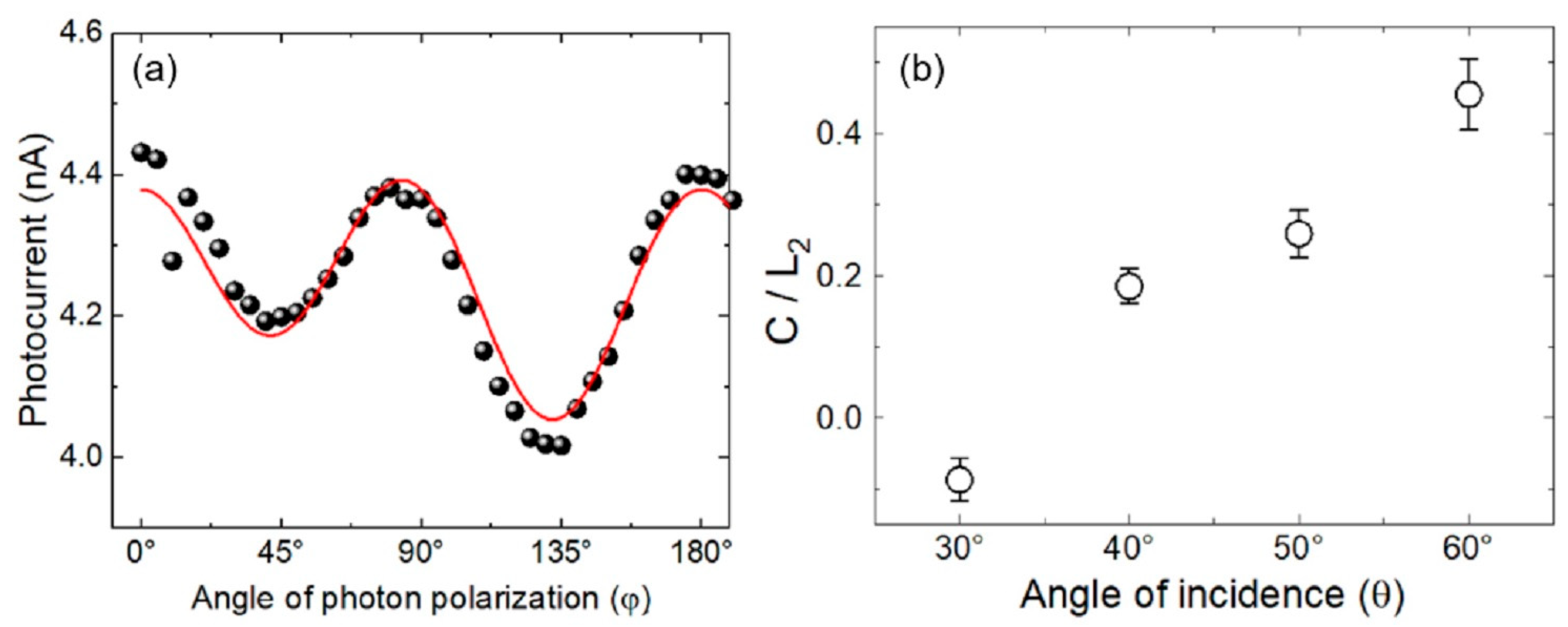
3.1. Phenomenology
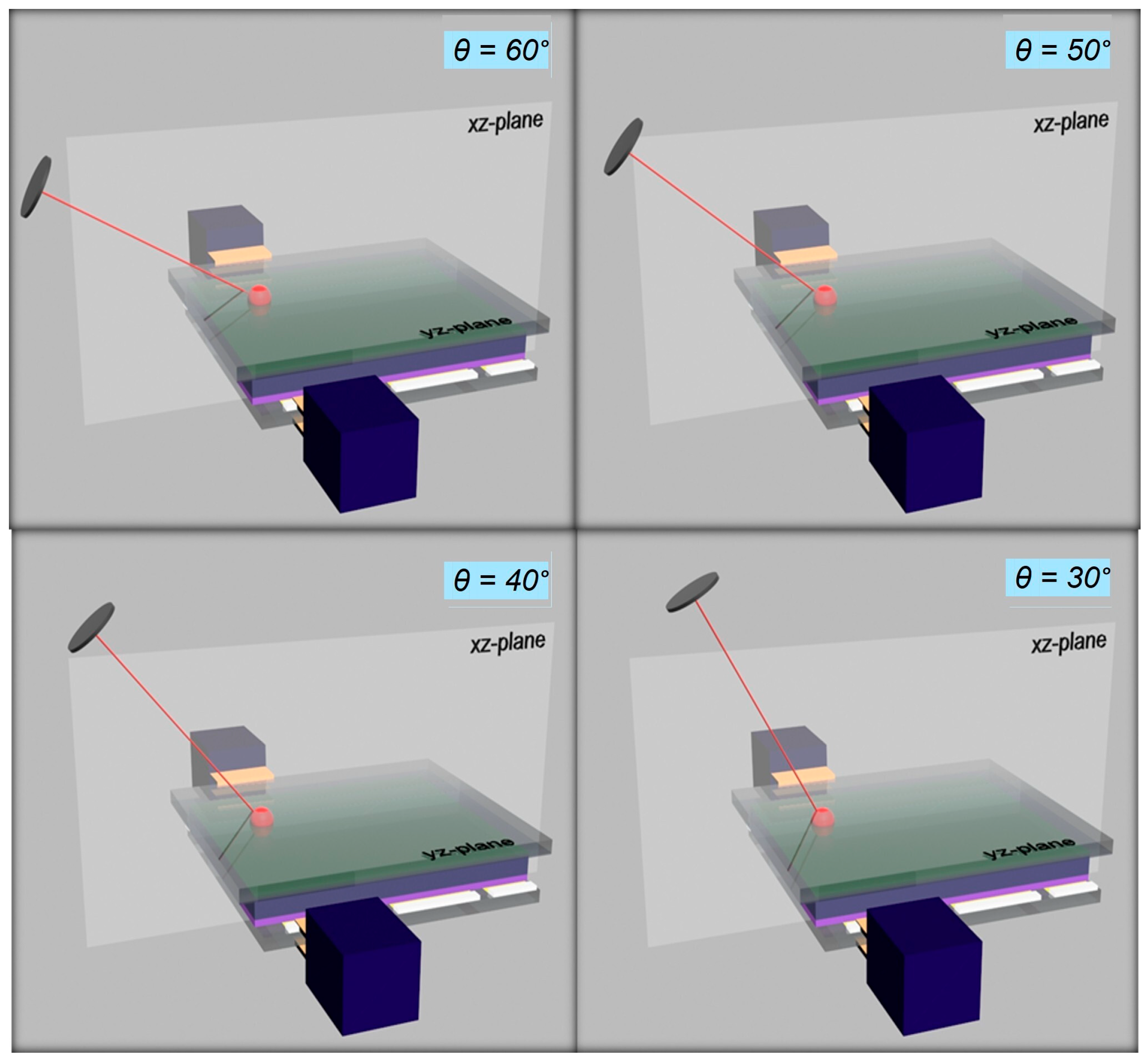
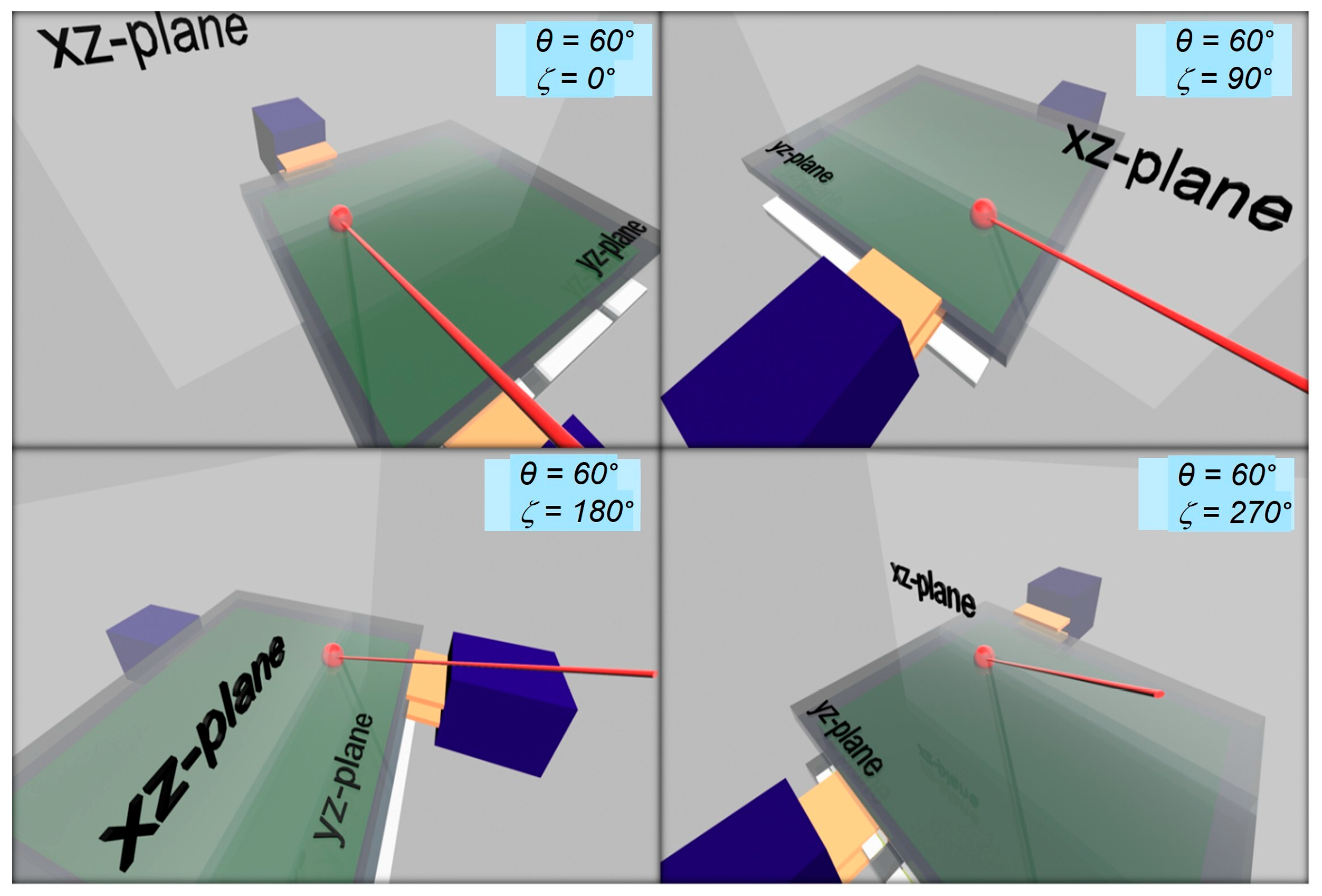
3.2. Light-Impinging Geometries on a Vertical Device Structure
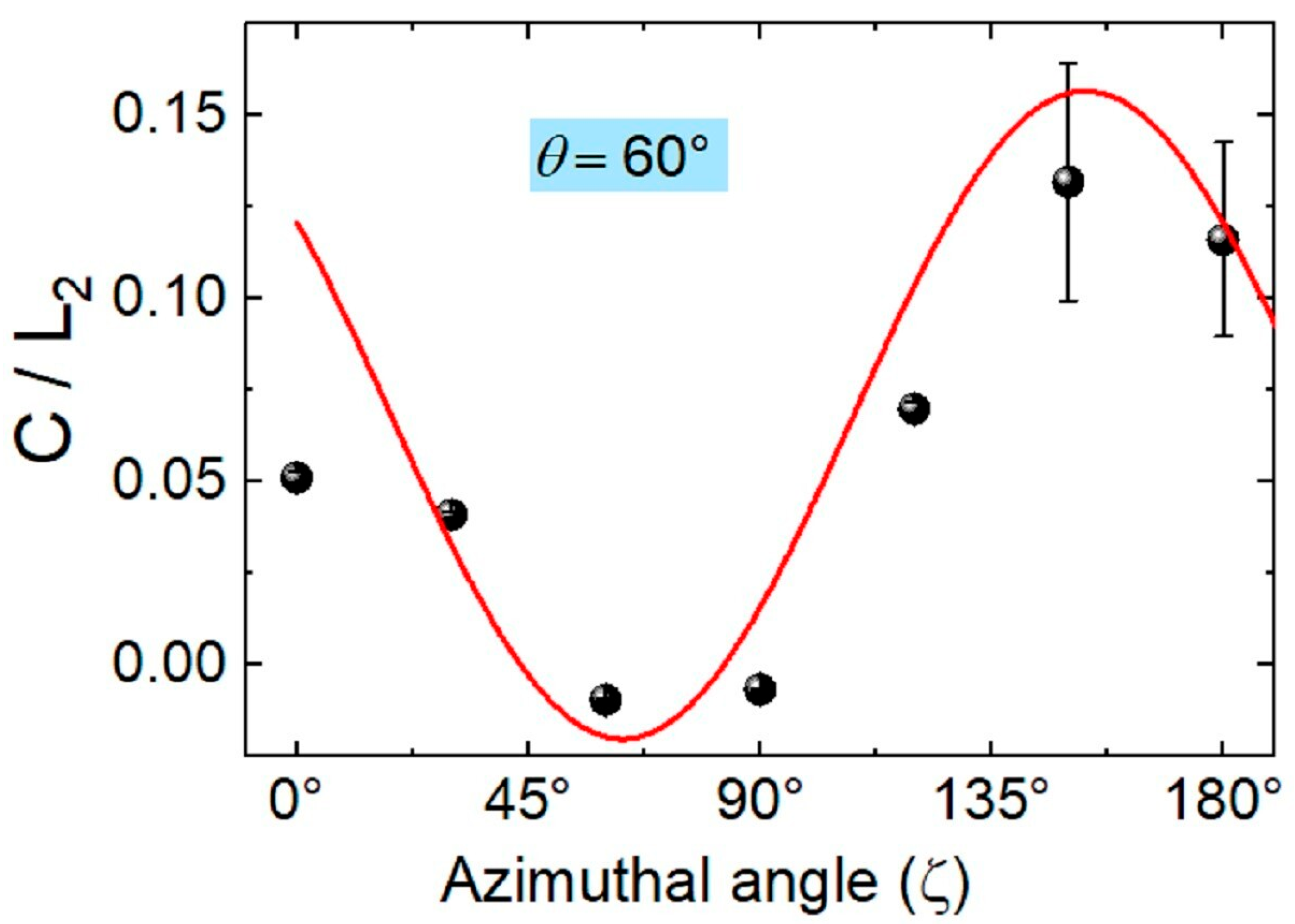
3.3. Nonlinear Photocurrent in an HOIP-Based Vertical Device
4. Discussion
5. Conclusions
Supplementary Materials
Author Contributions
Funding
Institutional Review Board Statement
Informed Consent Statement
Data Availability Statement
Acknowledgments
Conflicts of Interest
References
- Stenzel, O. Light-Matter Interaction: A Crash Course for Students of Optics, Photonics and Materials Science, 1st ed.; Springer Nature: New York, NY, USA, 2022; pp. 471–494. [Google Scholar] [CrossRef]
- Glass, A.M.; von der Linde, D.; Negran, T.J. High-voltage bulk photovoltaic effect and the photorefractive process in LiNbO3. Appl. Phys. Lett. 1974, 25, 233–235. [Google Scholar] [CrossRef]
- Koch, W.T.H.; Münser, R.; Ruppel, W.; Würfel, P. Bulk photovoltaic effect in BaTiO3. Solid State Commun. 1975, 17, 847–850. [Google Scholar] [CrossRef]
- Asnin, V.M.; Bakun, A.A.; Danishevskii, A.M.; Ivchenko, E.L.; Pikus, G.E.; Rogachev, A.A. “Circular” photogalvanic effect in optically active crystals. Solid State Commun. 1979, 30, 565–570. [Google Scholar] [CrossRef]
- von Blatz, R.; Kraut, W. Theory of the bulk photovoltaic effect in pure crystals. Phys. Rev. B 1981, 23, 5590–5596. [Google Scholar] [CrossRef]
- Belinicher, V.I.; Kanaev, I.F.; Malinovsky, V.K.; Sturman, B.I. Theory of photogalvanic effect in ferroelectrics. Ferroelectrics 1978, 22, 647–648. [Google Scholar] [CrossRef]
- Belinicher, V.I.; Sturman, B.I. The photogalvanic effect in media lacking a center of symmetry. Sov. Phys. Usp. 1980, 23, 199–223. [Google Scholar] [CrossRef]
- Belinicher, V.I. Space-Oscillating photocurrent in crystals without symmetry center. Phys. Lett. 1978, 66, 213–214. [Google Scholar] [CrossRef]
- Ivchenko, E.L.; Pikus, G.E. New photogalvanic effect in gyrotropic crystals. JETP Lett. 1978, 27, 604–608. [Google Scholar]
- Ganichev, S.D.; Prettl, W. Spin photocurrents in quantum wells. J. Phys. Condens. Matter. 2003, 15, R935–R983. [Google Scholar] [CrossRef]
- Glazov, M.M.; Ganichev, S.D. High frequency electric field induced nonlinear effects in graphene. Phys. Rep. 2014, 535, 101–138. [Google Scholar] [CrossRef]
- Bihlmayer, G.; Noël, P.; Vyalikh, D.V.; Chulkov, E.V.; Manchon, A. Rashba-like physics in condensed matter. Nat. Rev. Phys. 2022, 4, 642–659. [Google Scholar] [CrossRef]
- Kepenekian, M.; Even, J. Rashba and Dresselhaus couplings in halide perovskites: Accomplishments and opportunities for spintronics and spin−orbitronics. J. Phys. Chem. Lett. 2017, 8, 3362–3370. [Google Scholar] [CrossRef] [PubMed]
- Chen, J.; Koc, H.; Zhao, S.; Wang, K.; Chao, L.; Eginligil, M. Emerging nonlinear photocurrents in lead halide perovskites for spintronics. Materials 2024, 17, 1820. [Google Scholar] [CrossRef] [PubMed]
- Jiang, C.; Shalygin, V.A.; Panevin, V.Y.; Danilov, S.N.; Glazov, M.M.; Yakimova, R.; Lara-Avila, S.; Kubatkin, S.; Ganichev, S.D. Helicity-dependent photocurrents in graphene layers excited by midinfrared radiation of a CO2 laser. Phys. Rev. B 2013, 84, 125429. [Google Scholar] [CrossRef]
- Yuan, H.; Wang, X.; Lian, B.; Zhang, H.; Fang, X.; Shen, B.; Xu, G.; Xu, Y.; Zhang, S.-C.; Hwang, H.Y.; et al. Generation and electric control of spin–valley coupled circular photogalvanic current in WSe2. Nat. Nanotechnol. 2014, 9, 851–857. [Google Scholar] [CrossRef] [PubMed]
- Eginligil, M.; Cao, B.; Wang, Z.; Shen, X.; Cong, C.; Shang, J.; Soci, C.; Yu, T. Dichroic spin–valley photocurrent in monolayer molybdenum disulphide. Nat. Commun. 2015, 6, 7636. [Google Scholar] [CrossRef]
- Guan, H.; Tang, N.; Xu, X.; Shang, L.; Huang, W.; Fu, L.; Fang, X.; Yu, J.; Zhang, C.; Zhang, X.; et al. Photon wavelength dependent valley photocurrent in multilayer MoS2. Phys. Rev. B 2017, 96, 241304(R). [Google Scholar] [CrossRef]
- Quereda, J.; Ghiasi, T.S.; You, J.S.; van den Brink, J.; van Wees, B.J.; van der Waal, C.H. Symmetry regimes for circular photocurrents in monolayer MoSe2. Nat. Commun. 2018, 9, 3346. [Google Scholar] [CrossRef]
- Liu, L.; Lenferink, E.J.; Wei, G.; Stanev, T.K.; Speiser, N.; Stern, N.P. Electrical control of circular photogalvanic spin-valley photocurrent in a monolayer semiconductor. ACS Appl. Mater. Interfaces 2019, 11, 3334–3341. [Google Scholar] [CrossRef]
- Quereda, J.; Hidding, J.; Ghiasi, T.S.; van Wees, B.J.; van der Wal, C.H.; Guimarães, M.H.D. The role of device asymmetries and Schottky barriers on the helicity-dependent photoresponse of 2D phototransistors. npj 2D Mater. Appl. 2021, 5, 13. [Google Scholar] [CrossRef]
- McIver, J.; Hsieh, D.; Steinberg, H.; Jarillo-Herrero, P.; Gedik, N. Control over topological insulator photocurrents with light polarization. Nat. Nanotechnol. 2012, 7, 96–100. [Google Scholar] [CrossRef]
- Su, X.; Adamo, G.; Eginligil, M.; Krishnamoorthy, H.N.S.; Zheludev, N.I.; Soci, C. Topological insulator metamaterial with giant circular photogalvanic effect. Sci. Adv. 2021, 7, eabe5748. [Google Scholar] [CrossRef]
- Roy, S.; Manna, S.; Mitra, C.; Pal, B. Photothermal control of helicity-dependent current in epitaxial Sb2Te2Se topological insulator thin-films at ambient temperature. ACS Appl. Mater. Interfaces 2022, 14, 9909–9916. [Google Scholar] [CrossRef]
- Liang, Z.; Zhou, X.; Zhang, L.; Yu, X.; Lv, Y.; Song, X.; Zhou, Y.; Wang, H.; Wang, S.; Wang, T.; et al. Strong bulk photovoltaic effect in engineered edge-embedded van der Waals structures. Nat. Commun. 2023, 14, 4230. [Google Scholar] [CrossRef] [PubMed]
- Niesner, D.; Hauck, M.; Shrestha, S.; Levchuk, I.; Matt, G.J.; Osvet, A.; Batentschuk, M.; Brabec, C.; Weber, H.B.; Fauster, T. Structural fluctuations cause spin-split states in tetragonal (CH3NH3)PbI3 as evidenced by the circular photogalvanic effect. Proc. Natl. Acad. Sci. USA 2018, 115, 9509–9514. [Google Scholar] [CrossRef] [PubMed]
- Obraztsov, P.A.; Lyashenko, D.; Chizhov, P.A.; Konishi, K.; Nemoto, N.; Kuwata-Gonokami, M.; Welch, E.; Obraztsov, A.N.; Zakhidov, A. Ultrafast zero-bias photocurrent and terahertz emission in hybrid perovskites. Commun. Phys. 2018, 1, 14. [Google Scholar] [CrossRef]
- Liu, X.; Chanana, A.; Huynh, U.; Xue, F.; Haney, P.; Blair, S.; Jiang, X.; Vardeny, Z.V. Circular photogalvanic spectroscopy of Rashba splitting in 2D hybrid organic–inorganic perovskite multiple quantum wells. Nat. Commun. 2020, 11, 323. [Google Scholar] [CrossRef]
- Zhou, B.; Liang, L.; Ma, J.; Li, J.; Li, W.; Liu, Z.; Li, H.; Chen, R.; Li, D. Thermally assisted Rashba splitting and circular photogalvanic effect in aqueously synthesized 2D Dion–Jacobson perovskite crystals. Nano Lett. 2021, 21, 4584–4591. [Google Scholar] [CrossRef] [PubMed]
- Jia, R.; Jiang, J.; Zhang, L.; Hu, Y.; Pendse, S.; Guo, Y.; Si, J. Composition gradient-enabled circular photogalvanic effect in inogranic halide perovskites. Appl. Phys. Lett. 2022, 120, 211901. [Google Scholar] [CrossRef]
- Stadler, P.; Fogelström, M. Transport properties of vertical heterostructures under light irradiation. Phys. Rev. B 2022, 106, 085409. [Google Scholar] [CrossRef]
- Qin, W.; Xu, H.; Hu, B. Effects of spin states on photovoltaic actions in organo-metal halide perovskite solar cells based on circularly polarized photoexcitation. ACS Photonics 2017, 4, 2821–2827. [Google Scholar] [CrossRef]
- Wei, M.; Hao, X.; Saxena, A.B.; Qin, W.; Xie, S. Optical helicity-manipulated photocurrents and photovoltages in organic solar cells. J. Phys. Chem. C 2018, 122, 12566–12571. [Google Scholar] [CrossRef]
- Wang, J.; Lu, H.; Pan, X.; Xu, J.; Liu, H.; Liu, X.; Khanal, D.R.; Toney, M.F.; Beard, M.C.; Vardeny, Z.V. Spin-Dependent photovoltaic and photogalvanic responses of optoelectronic devices based on chiral two-dimensional hybrid organic−inorganic perovskites. ACS Nano 2021, 15, 588–595. [Google Scholar] [CrossRef]
- Dang, Y.; Tao, X. Recent progress of bulk photovoltaic effect in acentric single crystals and optoelectronic devices. Matter 2022, 5, 2659–2684. [Google Scholar] [CrossRef]
- Hui, W.; Chao, L.; Lu, H.; Xia, F.; Wei, Q.; Su, Z.; Niu, T.; Tao, L.; Du, B.; Li, D.; et al. Stabilizing black-phase formamidinium perovskite formation at room temperature and high humidity. Science 2021, 371, 1359–1364. [Google Scholar] [CrossRef]
- Wang, N.; Cheng, L.; Ge, R.; Zhang, S.; Miao, Y.; Zou, W.; Yi, C.; Sun, Y.; Yang, R.; Wei, Y.; et al. Perovskite light-emitting diodes based on solution-processed self-organized multiple quantum wells. Nat. Photon. 2016, 10, 699–704. [Google Scholar] [CrossRef]
- Eginligil, M.; Yu, T. Introduction to light polarization-dependent photocurrent—Phenomenology. In Second-Order Photogalvanic Photocurrents in 2D Materials, SpringerBriefs in Applied Sciences and Technology, 1st ed.; Demir, H.V., Govorov, A.O., Eds.; Springer: Singapore, 2024; Volume 1, pp. 1–19. [Google Scholar] [CrossRef]
- Clark Jones, R.A. New Calculus for the treatment of optical systems I. Description and discussion of the calculus. J. Opt. Soc. Am. 1941, 31, 488–493. [Google Scholar] [CrossRef]
- Yang, H.; Schmoranzerova, E.; Jang, P.; Nath, J.; Guillet, T.; Joumard, I.; Auffret, S.; Jamet, M.; Nemec, P.; Gaudin, G.; et al. Helicity dependent photoresistance measurement vs. beam-shift thermal gradient. Nat. Commun. 2022, 13, 6790. [Google Scholar] [CrossRef] [PubMed]
- Danishevskii, A.M.; Kastal’skii, A.A.; Ryvkin, S.M.; Yaroshetskii, I.D. Dragging of free carriers by photons in direct interband transitions in semiconductors. Sov. Phys. JETP 1970, 31, 292–295. [Google Scholar]
- Barlow, H.M. The Hall effect and its application to microwave power measurement. Proc. IRE 1958, 46, 1411–1413. [Google Scholar] [CrossRef]


Disclaimer/Publisher’s Note: The statements, opinions and data contained in all publications are solely those of the individual author(s) and contributor(s) and not of MDPI and/or the editor(s). MDPI and/or the editor(s) disclaim responsibility for any injury to people or property resulting from any ideas, methods, instructions or products referred to in the content. |
© 2025 by the authors. Licensee MDPI, Basel, Switzerland. This article is an open access article distributed under the terms and conditions of the Creative Commons Attribution (CC BY) license (https://creativecommons.org/licenses/by/4.0/).
Share and Cite
Koc, H.; Chen, J.; Gu, D.; Eginligil, M. Visualization of Light-Impinging Geometry in Nonlinear Photocurrents of Vertical Optoelectronic Devices. Materials 2025, 18, 3503. https://doi.org/10.3390/ma18153503
Koc H, Chen J, Gu D, Eginligil M. Visualization of Light-Impinging Geometry in Nonlinear Photocurrents of Vertical Optoelectronic Devices. Materials. 2025; 18(15):3503. https://doi.org/10.3390/ma18153503
Chicago/Turabian StyleKoc, Hacer, Jianbin Chen, Dawei Gu, and Mustafa Eginligil. 2025. "Visualization of Light-Impinging Geometry in Nonlinear Photocurrents of Vertical Optoelectronic Devices" Materials 18, no. 15: 3503. https://doi.org/10.3390/ma18153503
APA StyleKoc, H., Chen, J., Gu, D., & Eginligil, M. (2025). Visualization of Light-Impinging Geometry in Nonlinear Photocurrents of Vertical Optoelectronic Devices. Materials, 18(15), 3503. https://doi.org/10.3390/ma18153503