
Unveiling Thickness-Dependent Oxidation Effect on Optical Response of Room Temperature RF-Sputtered Nickel Ultrathin Films on Amorphous Glass: An Experimental and FDTD Investigation

 ,
,  , , ,
, , ,  , , and
Abstract

1. Introduction
2. Materials and Methods
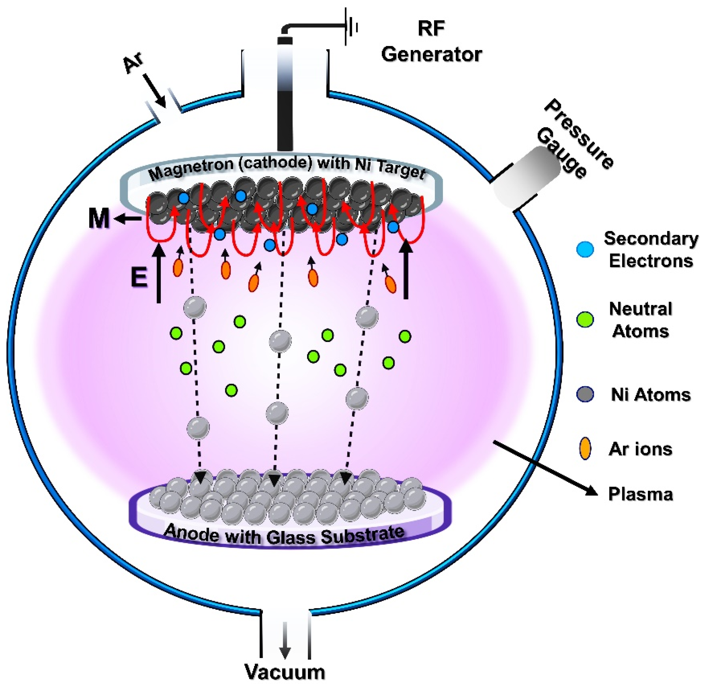
2.1. Experimental—RF Sputtering
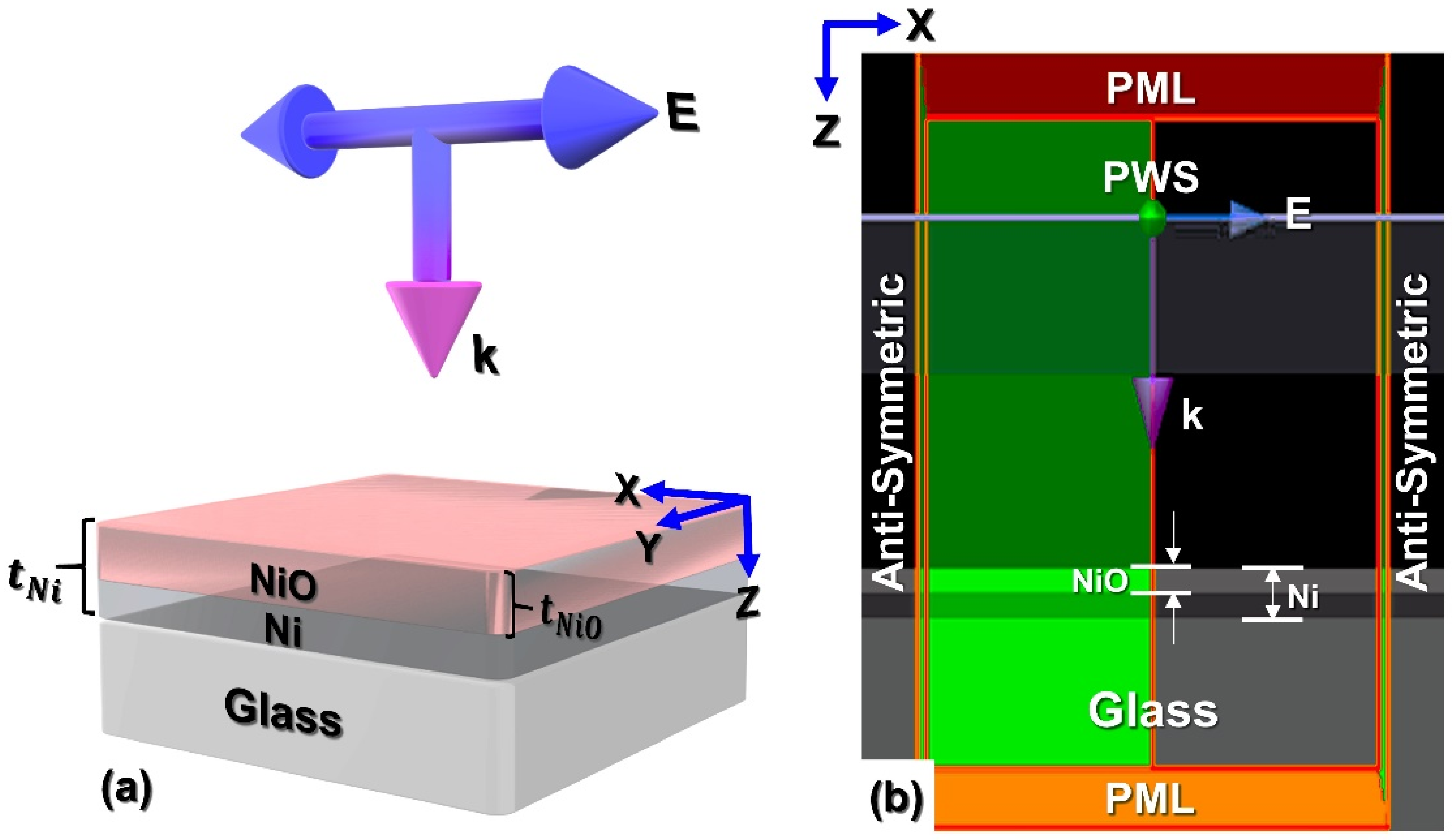
2.2. FDTD Simulation Mechanism
3. Results and Discussion
3.1. Experimental
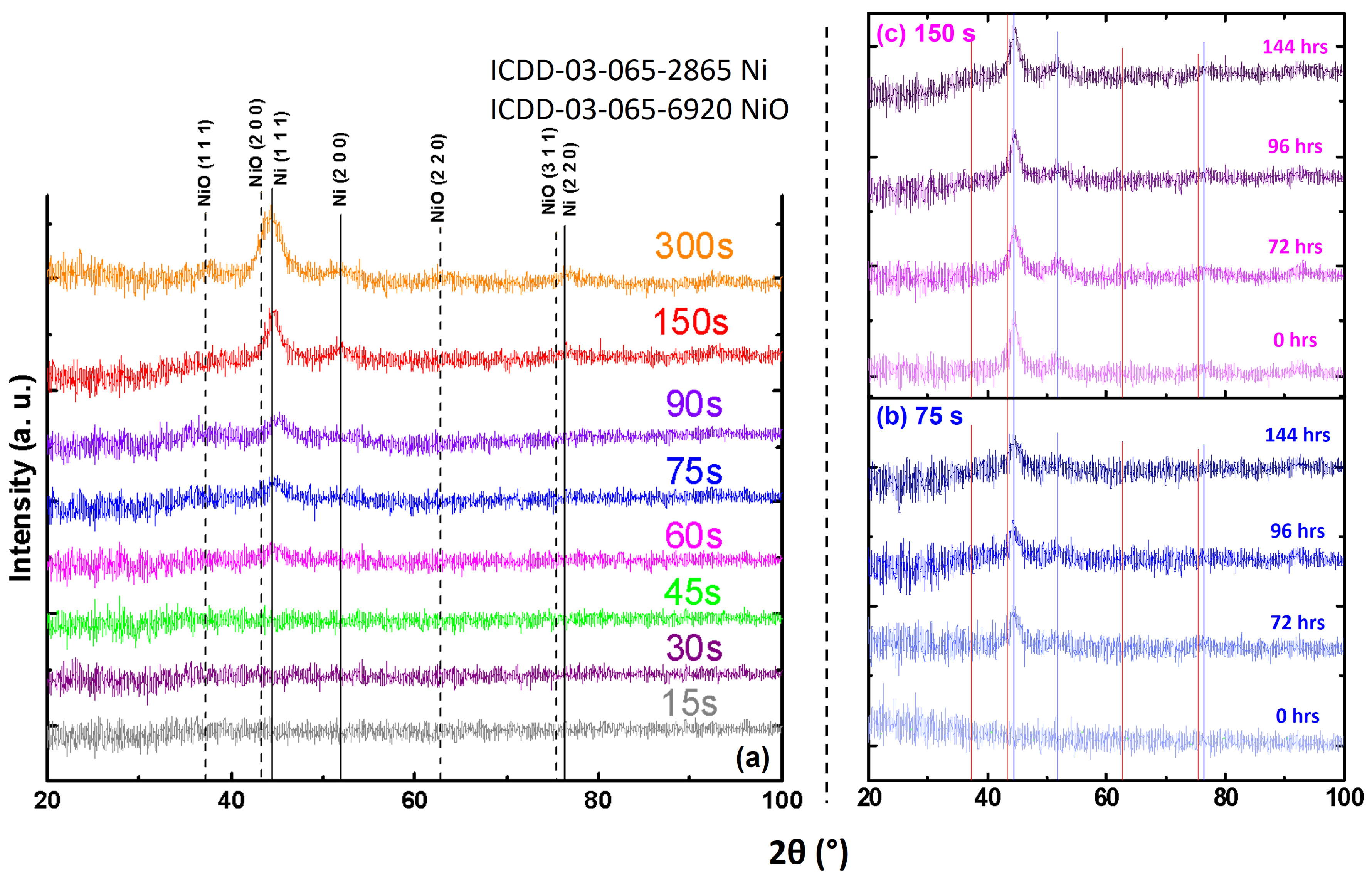
3.1.1. Structural Analysis (XRD)
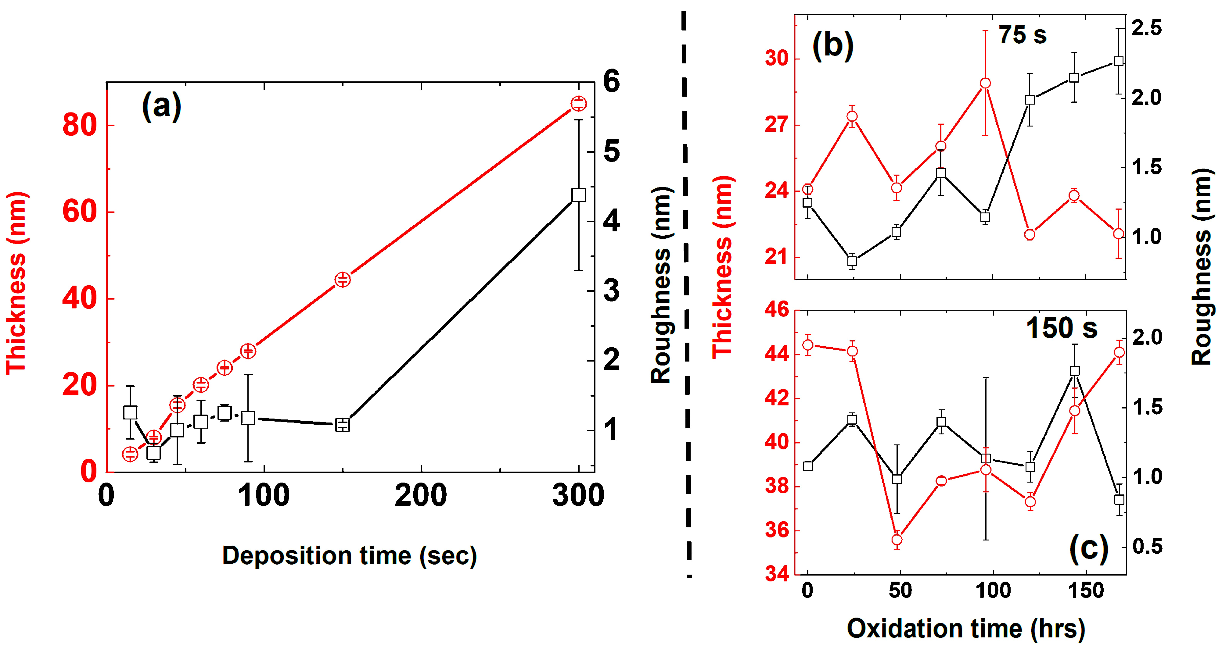
3.1.2. Thickness and Roughness—AFM Analysis
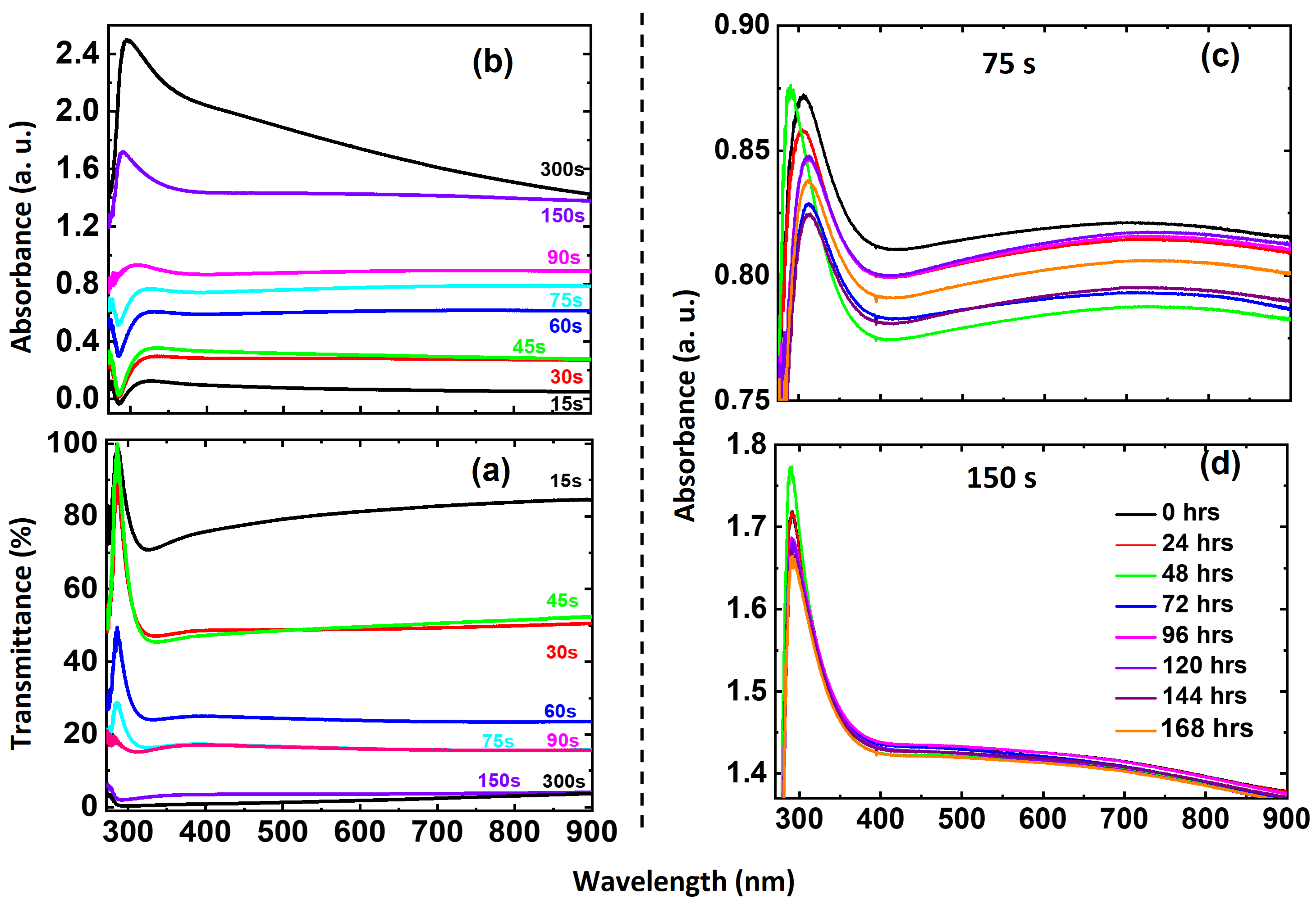
3.1.3. Optical Properties: Transmittance and Absorbance
3.2. FDTD Simulations
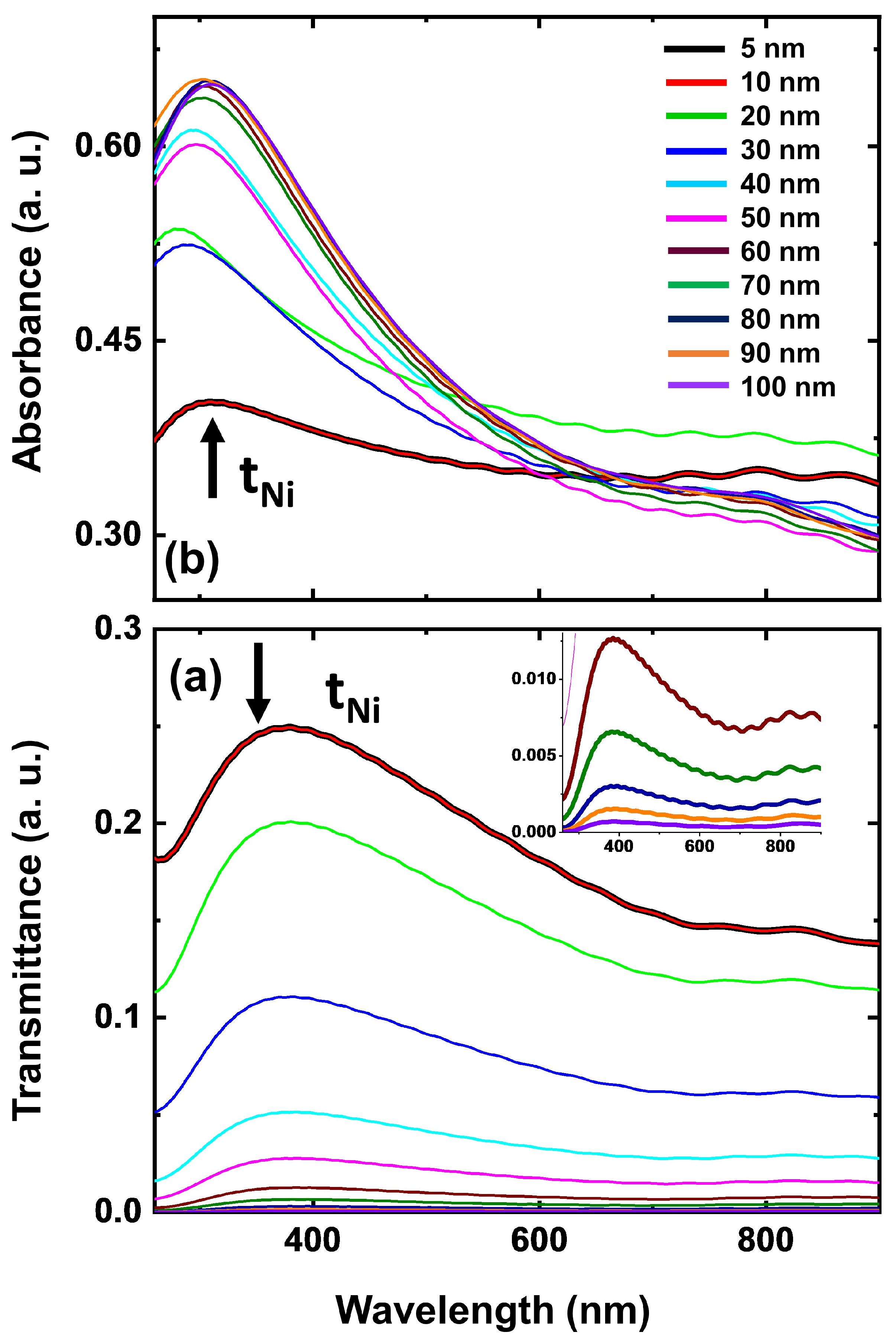
3.2.1. Thickness-Dependent Optical Analysis—Ni-NiO Thin Films
3.2.2. Optical Response (Transmittance and Absorbance) of Ni Thin Films–FDTD Simulations
3.3. Simulation and Experimental Comparative Analysis:
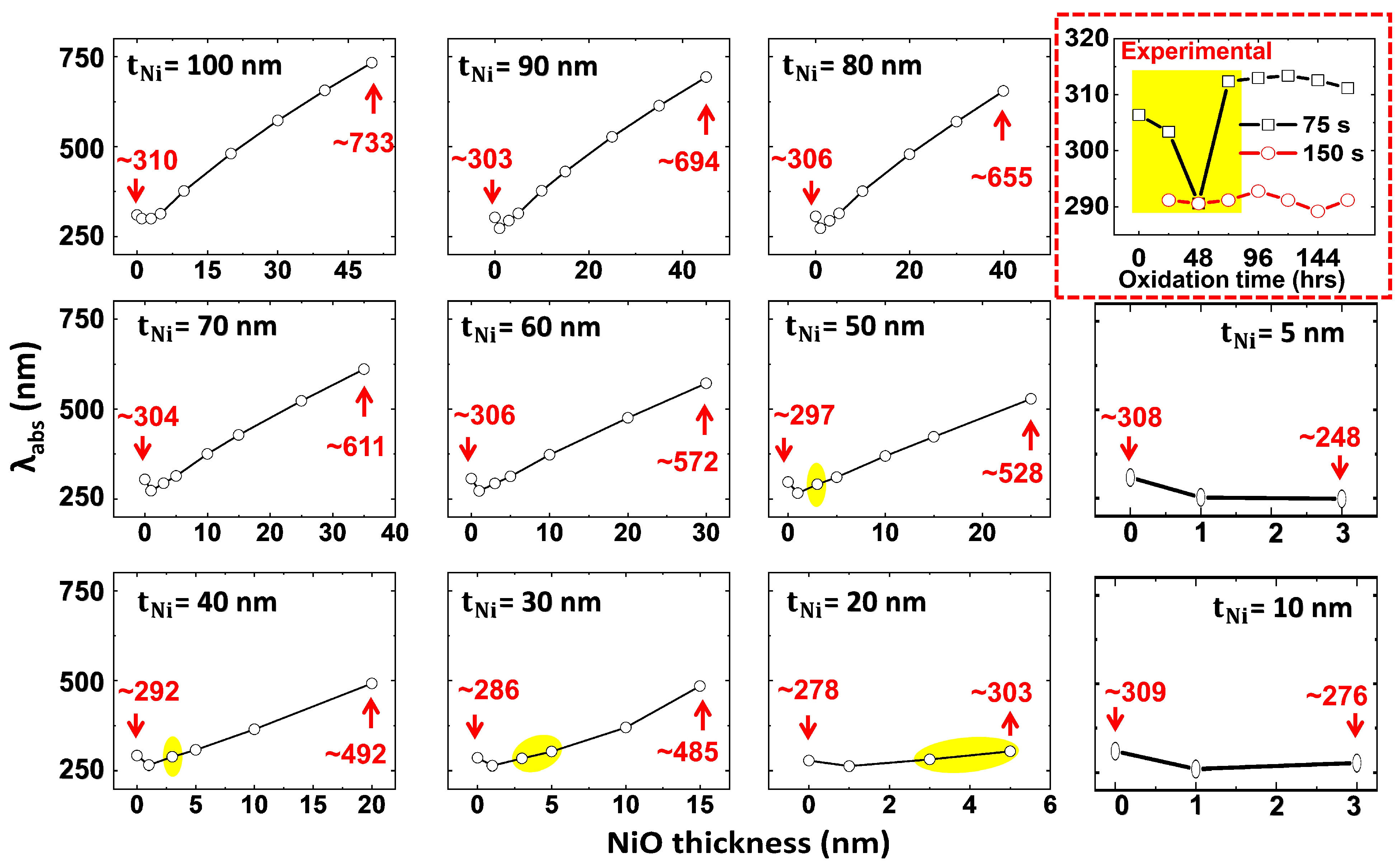
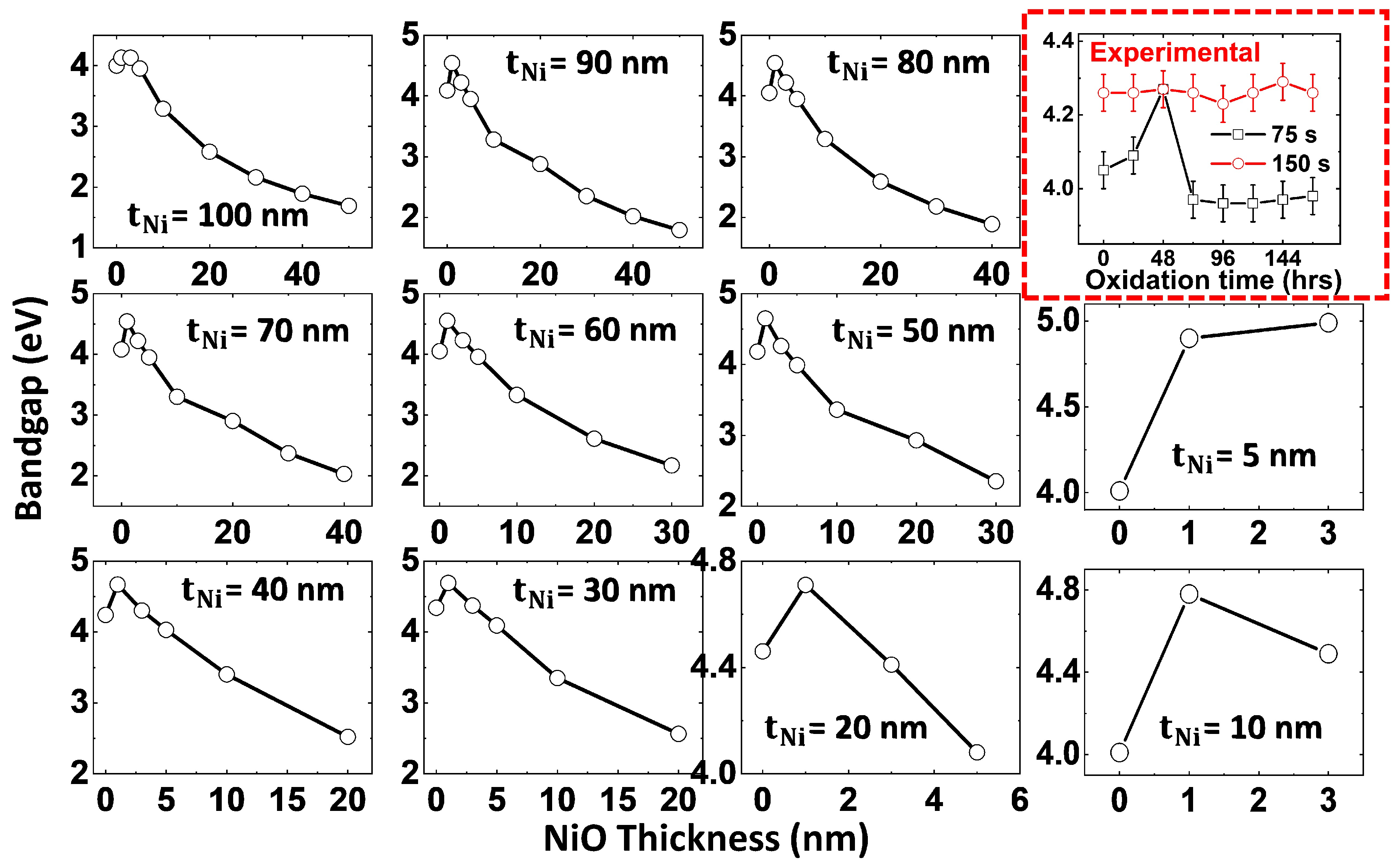
3.3.1. Thickness Dependence on Plasmonic Peak and Bandgap
3.3.2. Correlation Between Thickness-Dependent Oxidation and Plasmonic Peak Tunability in Ni-NiO Ultrathin Films—FDTD Simulations
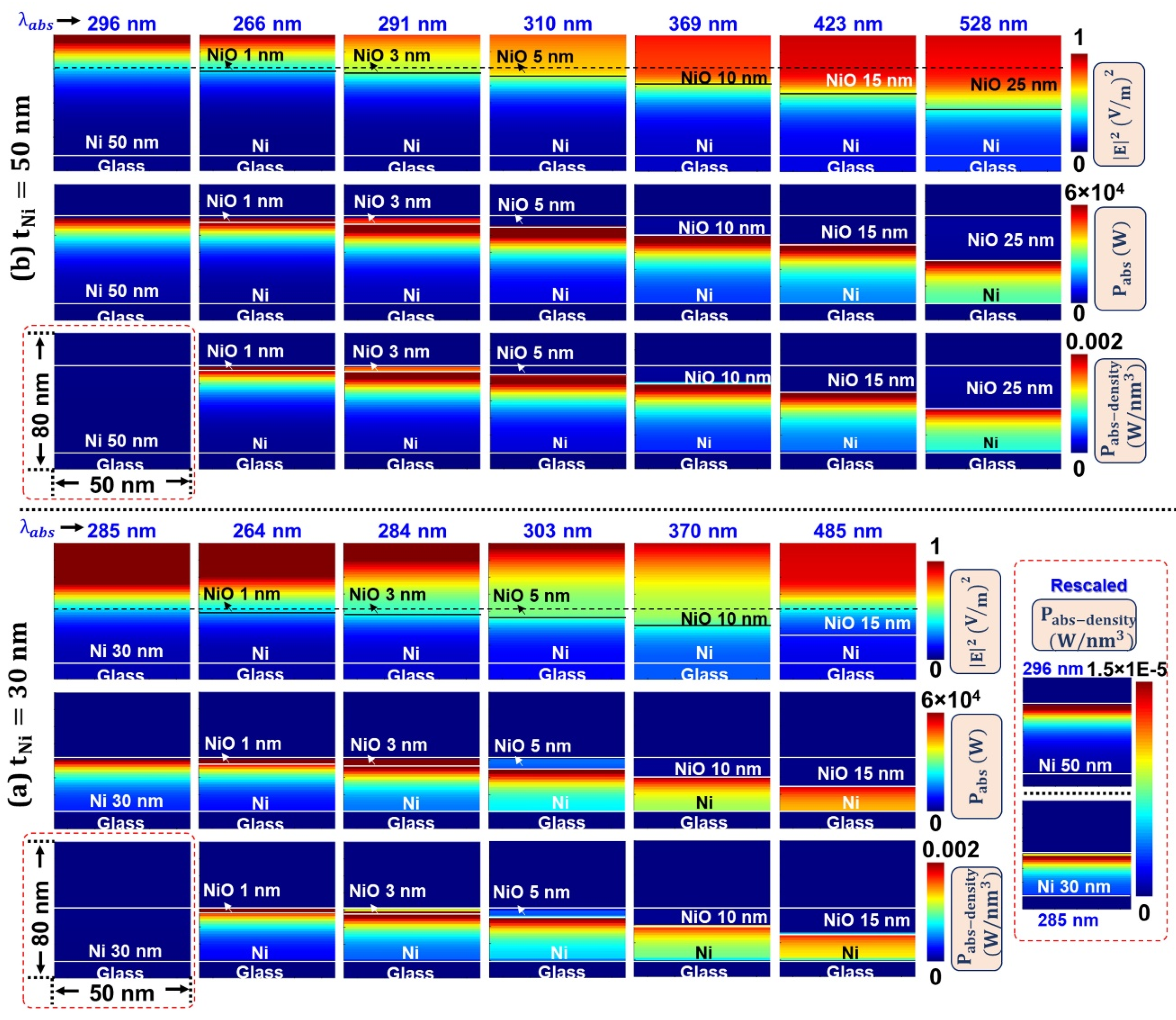
3.4. Oxidation Induced Electric Field Localization and Self-Heating Effects—FDTD Simulations
4. Conclusions
Supplementary Materials
Author Contributions
Funding
Institutional Review Board Statement
Informed Consent Statement
Data Availability Statement
Conflicts of Interest
Abbreviations
| RF | Radio Frequency |
| FDTD | Finite Difference Time Domain |
| SPR | Surface Plasmon Resonance |
| TCEs | Transparent Conductive Electrodes |
| MO | Magneto-Optic |
| SPs | Surface Plasmons |
| EM | Electromagnetic |
| SPPs | Surface Plasmon-Polaritons |
| LSPs | Localized SPs |
| SAW-FMR | Surface Acoustic Wave-driven Ferromagnetic Resonance |
| RT | Room Temperature |
| FM | Ferromagnetic |
| UV | Ultraviolet |
| LSPR | Localized Surface Plasmon Resonance |
| IR | Infrared |
| XRD | X-ray diffraction |
| AFM | Atomic Force Microscopy |
| PWS | Plane Wave Source |
| PML | Perfectly Matched absorbing Layer |
| BCs | Boundary Conditions |
| Rq | Root-Mean-Square |
References
- Clavero, C.; Yang, K.; Skuza, J.R.; Lukaszew, R.A. Magnetic field modulation of intense surface plasmon polaritons. Opt. Express. 2010, 18, 7743–7752. [Google Scholar] [CrossRef] [PubMed]
- Frolov, A.Y.; Shcherbakov, M.R.; Fedyanin, A.A. Dark mode enhancing magneto-optical Kerr effect in multilayer magnetoplasmonic crystals. Phys. Rev. B 2020, 101, 045409. [Google Scholar] [CrossRef]
- Rizal, C.; Niraula, B.; Ho, H.; Bio-Magnetoplasmonics, W.L. Emerging Biomedical Technologies and Beyond. J. Nanomed. Res. 2016, 3, 00059. [Google Scholar] [CrossRef]
- Pourjamal, S.; Kataja, M.; Maccaferri, N.; Vavassori, P.; van Dijken, S. Tunable magnetoplasmonics in lattices of Ni/SiO2/Au dimers. Sci. Rep. 2019, 9, 9907. [Google Scholar] [CrossRef]
- Vo, T.S.; Surabhi, S.; Luong, C.H.; Yoon, S.G.; Lee, K.D.; Park, B.G.; Jeong, J.R. Magnetic resonance absorption in isolated metal/insulator/metal nanodot arrays with transmission geometry. Curr. Appl. Phys. 2015, 15, 844–849. [Google Scholar] [CrossRef]
- Jeon, S.; Sung, S.K.; Jang, E.H.; Jeong, J.; Surabhi, S.; Choi, J.H.; Jeong, J.R. Multilayer metal-oxide-metal nanopatterns via nanoimprint and strip-off for multispectral resonance. Appl. Surf. Sci. 2018, 428, 280–288. [Google Scholar] [CrossRef]
- Rezaeian, A.; Farzad, M.H. Magneto-optical heterostructures with second resonance of transverse magneto-optical Kerr effect. Sci. Rep. 2024, 14, 3493. [Google Scholar] [CrossRef]
- Kretschmann, E.; Raether, H. Radiative Decay of Non Radiative Surface Plasmons Excited by Light. Zeitschrift Fur Naturforsch. A 1968, 23, 2135–2136. [Google Scholar] [CrossRef]
- Yamane, H.; Yanase, S.; Hasegawa, T.; Kobayashi, M.; Yasukawa, Y. Polarization transformation and destructive interference on subwavelength magnetic domains in magneto-plasmonic systems. Sci. Rep. 2022, 12, 13871. [Google Scholar] [CrossRef]
- Borah, R.; Ninakanti, R.; Bals, S.; Verbruggen, S.W. Plasmon resonance of gold and silver nanoparticle arrays in the Kretschmann (attenuated total reflectance) vs. direct incidence configuration. Sci. Rep. 2022, 12, 15738. [Google Scholar] [CrossRef]
- McPherson, D.J.; Supansomboon, S.; Zwan, B.; Keast, V.J.; Cortie, D.L.; Gentle, A.; Dowd, A.; Cortie, M.B. Strategies to control the spectral properties of Au–Ni thin films. Thin Solid Films 2014, 551, 200–204. [Google Scholar] [CrossRef]
- Van, P.C.; Surabhi, S.; Quoc, V.D.; Lee, J.W.; Tae, C.C.; Kuchi, R.; Jeong, J.-R. Broadband tunable plasmonic substrate using self-assembled gold–silver alloy nanoparticles. Curr. Appl. Phys. 2019, 19, 1245–1251. [Google Scholar] [CrossRef]
- Coviello, V.; Badocco, D.; Pastore, P.; Fracchia, M.; Ghigna, P.; Martucci, A.; Forrer, D.; Amendola, V. Accurate prediction of the optical properties of nanoalloys with both plasmonic and magnetic elements. Nat. Commun. 2024, 15, 834. [Google Scholar] [CrossRef] [PubMed]
- Assadillayev; Faniayeu, I.; Dmitriev, A.; Raza, S.; Assadillayev, A.; Raza, S.; Faniayeu, I.; Dmitriev, A. Nanoscale Engineering of Optical Strong Coupling inside Metals. Adv. Opt. Mater. 2023, 11, 2201971. [Google Scholar] [CrossRef]
- Potočnik, J.; Novaković, M.; Popović, M. Thickness-dependent growth of Ni vertical columns deposited by GLAD method: Study on the microstructural and optical properties. Opt. Mater. 2024, 154, 115665. [Google Scholar] [CrossRef]
- Kim, H.J.; Song, M.; Jeong, J.H.; Kim, C.S.; Surabhi, S.; Jeong, J.R.; Kim, D.H.; Choi, D.G. Highly efficient and stable cupronickel nanomesh electrode for flexible organic photovoltaic devices. J. Power Sources 2016, 331, 22–25. [Google Scholar] [CrossRef]
- Weisenberg, M.; Aslan, K.; Hortle, E.; Geddes, C.D. Directional surface plasmon coupled chemiluminescence from nickel thin films: Fixed angle observation. Chem. Phys. Lett. 2009, 473, 120–125. [Google Scholar] [CrossRef]
- Grilli, M.L.; Di Sarcina, I.; Bossi, S.; Rinaldi, A.; Pilloni, L.; Piegari, A. Ultrathin and stable Nickel films as transparent conductive electrodes. Thin Solid Films 2015, 594, 261–265. [Google Scholar] [CrossRef]
- Schuermans, S.; Martin, J.; Moussy, J.-B.; Plain, J.; Maurer, T. Plasmon/interband transitions coupling in the UV from large scale nanostructured Ni films. Opt. Mater. Express 2017, 7, 1787–1793. [Google Scholar] [CrossRef]
- Ravikumar, P.; Taparia, D.; Alagarsamy, P. Thickness-Dependent Thermal Oxidation of Ni into NiO Thin Films. J. Supercond. Nov. Magn. 2018, 31, 3761–3775. [Google Scholar] [CrossRef]
- Cheng, W.; Ge, W.; Yang, Q.; Qu, X. Study on the corrosion properties of nanocrystalline nickel electrodepositied by reverse pulse current. Appl. Surf. Sci. 2013, 276, 604–608. [Google Scholar] [CrossRef]
- Unutulmazsoy, Y.; Merkle, R.; Fischer, D.; Mannhart, J.; Maier, J. The oxidation kinetics of thin nickel films between 250 and 500 °C. Phys. Chem. Chem. Phys. 2017, 19, 9045–9052. [Google Scholar] [CrossRef]
- Lisoni, J.G.; Goux, L.; Hoffmann, T.; Diaz-Droguett, D.E.; Jurczak, M. Influence of the microstructure on the oxidation of Ni thin films. Corros. Sci. 2012, 59, 282–289. [Google Scholar] [CrossRef]
- Inoue, N.; Yasuoka, Y. Properties of nickel oxide films grown by sputter oxidation. Vacuum 1984, 34, 687–691. [Google Scholar] [CrossRef]
- Hajakbari, F.; Rashvand, S.; Hojabri, A. Effect of plasma oxidation parameters on physical properties of nanocrystalline nickel oxide thin films grown by two-step method: DC sputtering and plasma oxidation. J. Theor. Appl. Phys. 2019, 13, 365–373. [Google Scholar] [CrossRef]
- Hajakbari, F. Characterization of nanocrystalline nickel oxide thin films prepared at different thermal oxidation temperatures. J. Nanostruct. Chem. 2020, 10, 97–103. [Google Scholar] [CrossRef]
- Lapitskaya, V.; Trukhan, R.; Kuznetsova, T.; Solovjov, J.; Chizhik, S.; Pilipenko, V.; Liutsko, K.; Nasevich, A.; Douhal, M. Microstructure and Properties of Thin-Film Submicrostructures Obtained by Rapid Thermal Treatment of Nickel Films on Silicon. Surfaces 2024, 7, 196–207. [Google Scholar] [CrossRef]
- Lagrow, A.P.; Alyami, N.M.; Lloyd, D.C.; Bakr, O.M.; Boyes, E.D.; Gai, P.L. In situ oxidation and reduction of triangular nickel nanoplates via environmental transmission electron microscopy. J. Microsc. 2018, 269, 161–167. [Google Scholar] [CrossRef]
- Testov; Komlev, A.E.; Gareev, K.G.; Khmelnitskiy, I.K.; Luchinin, V.V.; Sevost’yanov, E.N.; Testov, I.O. Providing a Specified Level of Electromagnetic Shielding with Nickel Thin Films Formed by DC Magnetron Sputtering. Coatings 2021, 11, 1455. [Google Scholar] [CrossRef]
- Jeon, Y.S.; Park, N.G. Nickel Oxide Thin Films Formed from the pH-Adjusted Solutions for Inverted Perovskite Solar Cells. ACS Energy Lett. 2025, 10, 1266–1274. [Google Scholar] [CrossRef]
- Kalayci, T. Investigation of Cap and Buffer Layer Effect in Co/Ni Thin Films by Ferromagnetic Resonance Technique. Karadeniz Fen Bilim. Derg. 2023, 13, 724–733. [Google Scholar] [CrossRef]
- Hidrogo-Rico, M.A.; Nedev, N.; Horley, P.; Mendívil, M.I.; Castillo-Saenz, J.; Martínez-Guerra, E.; Juarez-Perez, E.J.; Aguirre-Tostado, F.S.; Susarrey-Arce, A.; Martínez-Guerra, E. Tailoring Nickel Oxide Thin Films: Comparative Study of Oxidizing Agents in Thermal and Plasma-Enhanced Atomic Layer Deposition. ACS Omega 2024, 10, 422–438. [Google Scholar] [CrossRef]
- Rattanasakulthong, W.; Sirisangsawang, P.; Pinitsoontorn, S.; Sirisathitkul, C. Dependence of Hysteresis Loops on Thickness of Thin Nickel Films Prepared by RF Sputtering. Adv. Mater. Res. 2011, 335–336, 1443–1447. [Google Scholar] [CrossRef]
- Salhi, M.; Abaidia, S.E.K.; Mammeri, S.; Bouaouina, B. Sputter deposition of Titanium and Nickel thin films in radio frequency magnetron discharge characterized by optical emission spectroscopy and by Rutherford backscattering spectrometry. Thin Solid Films 2017, 629, 22–27. [Google Scholar] [CrossRef]
- Teixeira, F.L.; Sarris, C.; Zhang, Y.; Na, D.Y.; Berenger, J.P.; Su, Y.; Okoniewski, M.; Chew, W.C.; Backman, V.; Simpson, J.J. Finite-difference time-domain methods. Nat. Rev. Methods Primers 2023, 3, 75. [Google Scholar] [CrossRef]
- Ahmed, A.A.A.; Alahsab, E.A.A.; Abdulwahab, A.M. The influence of Zn and Mg doping on the structural and optical properties of NiO nano-structures for optoelectronic applications. Results Phys. 2021, 22, 103938. [Google Scholar] [CrossRef]
- Minisha, S.; Johnson, J.; Wabaidur, S.M.; Gupta, J.K.; Aftab, S.; Siddiqui, M.R.; Lai, W.C. Synthesis and Characterizations of Fe-Doped NiO Nanoparticles and Their Potential Photocatalytic Dye Degradation Activities. Sustainability 2023, 15, 14552. [Google Scholar] [CrossRef]
- Ahmad, N.; Stokes, J.; Fox, N.A.; Teng, M.; Cryan, M.J. Ultra-thin metal films for enhanced solar absorption. Nano Energy 2012, 1, 777–782. [Google Scholar] [CrossRef]
- Duraisamy, N.; Kandiah, K.; Rajendran, R.; Prabhu, S.; Ramesh, R.; Dhanaraj, G. Electrochemical and photocatalytic investigation of nickel oxide for energy storage and wastewater treatment. Res. Chem. Intermed. 2018, 44, 5653–5667. [Google Scholar] [CrossRef]
- Sharma, V.; Chotia, C.; Tarachand; Ganesan, V.; Okram, G.S. Influence of particle size and dielectric environment on the dispersion behaviour and surface plasmon in nickel nanoparticles. Phys. Chem. Chem. Phys. 2017, 19, 14096–14106. [Google Scholar] [CrossRef]
- Abu-Safe, H.H.; Al-Esseili, R.; Al-Taani, H.; El-Nasser, H.; Refaei, M.; Sarollahi, M.; Alhelais, R.; Zamani-Alavijeh, M.; Ware, M.E. The nonlinear optical properties of nickel nano-films in the cw regime: Proposed model. Opt. Mater. 2021, 121, 111531. [Google Scholar] [CrossRef]
- Amekura, H.; Takeda, Y.; Kitazawa, H.; Kishimoto, N. Resonance energy of surface plasmon of nickel nanoparticles in silica glasses. Phot. Process. Microelectron. Photonics II 2003, 4977, 639–647. [Google Scholar] [CrossRef]
- Pham, T.K.H.; Tran, B.Q.; Nguyen, K.B.; Pham, N.Y.N.; Nguyen, T.H.Y.; Nguyen, A.H.-T.; Nguyen, N.P.; Ngo, H.D.; Pham, H.P. Oxygen partial pressure effects on nickel oxide thin films and NiO/Si diode performance. Mater. Adv. 2025, 6, 1719–1725. [Google Scholar] [CrossRef]
- Barala, S.; Panda, S.A.; Gangopadhyay, S. Growth and Characterization of NiO Thin Films for Selective Detection of Formaldehyde Vapor. Phys. Status Solidi 2024, 2400695. [Google Scholar] [CrossRef]
- Lahiji, F.A.F.; Bairagi, S.; Magnusson, R.; Sortica, M.A.; Primetzhofer, D.; Ekström, E.; Paul, B.; le Febvrier, A.; Eklund, P. Growth and optical properties of NiO thin films deposited by pulsed dc reactive magnetron sputtering. J. Vac. Sci. Technol. A 2023, 41, 063402. [Google Scholar] [CrossRef]
- Benedet, M.; Maccato, C.; Pagot, G.; Invernizzi, C.; Sada, C.; Di Noto, V.; Rizzi, G.A.; Fois, E.; Tabacchi, G.; Barreca, D. Growth of NiO Thin Films in the Presence of Water Vapor: Insights from Experiments and Theory. J. Phys. Chem. C 2023, 127, 22304–22314. [Google Scholar] [CrossRef]
- Timoshnev, S.; Kazakin, A.; Shubina, K.; Andreeva, V.; Fedorenko, E.; Koroleva, A.; Zhizhin, E.; Koval, O.; Kurinnaya, A.; Shalin, A.; et al. Annealing Temperature Effect on the Physical Properties of NiO Thin Films Grown by DC Magnetron Sputtering. Adv. Mater. Interfaces 2024, 11, 815. [Google Scholar] [CrossRef]
- Mahmoud, S.A.; Shereen, A.; Tarawnh, M.A. Structural and Optical Dispersion Characterisation of Sprayed Nickel Oxide Thin Films. J. Mod. Phys. 2011, 2, 1178–1186. [Google Scholar] [CrossRef]
- Rhodes, C.; Franzen, S.; Maria, J.-P.; Losego, M.; Leonard, D.N.; Laughlin, B.; Duscher, G.; Weibel, S. Surface plasmon resonance in conducting metal oxides. J. Appl. Phys. 2006, 100, 054905. [Google Scholar] [CrossRef]
- Wooten, F. Optical Properties Measurement Techniques Solar Energy Materials Special Issue; Academic Press: New York, NY, USA; London, UK, 1972. [Google Scholar]
- Zaouche, C. Electrical and Magnetic Properties of Nanostructured NiO Thin Films Prepared by Spray Pyrolysis Method. Biomed. J. Sci. Tech. Res. 2023, 52, 43761–43766. [Google Scholar] [CrossRef]
- Oluwabi, A.T.; Spalatu, N.; Maticiuc, N.; Katerski, A.; Mere, A.; Krunks, M.; Acik, I.O. Combinative solution processing and Li doping approach to develop p-type NiO thin films with enchanced electrical properties. Front. Mater. 2023, 10. [Google Scholar] [CrossRef]
- Kashir, A.; Jeong, H.-W.; Lee, G.-H.; Mikheenko, P.; Jeong, Y.H. Dielectric Properties of Strained Nickel Oxide Thin Films. J. Korean Phys. Soc. 2019, 74, 984–988. [Google Scholar] [CrossRef]
- Abubakar, D.; Ahmed, N.M.; Mahmud, S. Structural, Electrical and Optical Properties of NiO Nanostructured Growth Using Thermal Wet Oxidation of Nickel Metal Thin Film. J. Nano Res. 2016, 49, 56–65. [Google Scholar] [CrossRef]
- Lin, Z.; Du, C.; Yan, B.; Wang, C.; Yang, G. Two-dimensional amorphous NiO as a plasmonic photocatalyst for solar H2 evolution. Nat. Commun. 2018, 9, 1–11. [Google Scholar] [CrossRef]
- Bhakta, S.; Panda, R.; Sahoo, P.K. Third-order non-linear optical switching and threshold limiting of NiO thin films. Sci. Rep. 2024, 14, 22767. [Google Scholar] [CrossRef]


| S. No. | Deposition Time (s) | Thickness (nm) | Roughness (nm) | Grain Size (nm) |
|---|---|---|---|---|
| 1 | 15 | 4.16 ± 0.63 | 1.26 ± 0.38 | - |
| 2 | 30 | 7.99 ± 0.29 | 0.68 ± 0.14 | - |
| 3 | 45 | 15.48 ± 0.67 | 1.01 ± 0.50 | - |
| 4 | 60 | 20.16 ± 0.54 | 1.13 ± 0.31 | - |
| 5 | 75 | 24.09 ± 0.23 | 1.25 ± 0.12 | - |
| 6 | 90 | 27.96 ± 0.21 | 1.18 ± 0.63 | 33.53 ± 1.9 |
| 7 | 150 | 44.43 ± 0.48 | 1.08 ± 0.04 | 41.76 ± 1.2 |
| 8 | 300 | 85.04 ± 0.88 | 4.38 ± 1.08 | 25.83 ± 0.4 |
| S. No. | Ni Thickness (nm) | NiO Thickness (nm) |
|---|---|---|
| 1 | 5 | 1, 3 |
| 2 | 10 | 1, 3, 5 |
| 3 | 20 | 1, 3, 5, 10 |
| 4 | 30 | 1, 3, 5, 10, 15 |
| 5 | 40 | 1, 3, 5, 10, 20 |
| 6 | 50 | 1, 3, 5, 10, 15, 25 |
| 7 | 60 | 1, 3, 5, 10, 20, 30 |
| 8 | 70 | 1, 3, 5, 10, 15, 25, 35 |
| 9 | 80 | 1, 3, 5, 10, 20, 30, 40 |
| 10 | 90 | 1, 3, 5, 10, 15, 25, 35, 45 |
| 11 | 100 | 1, 3, 5, 10, 20, 30, 40, 50 |
Disclaimer/Publisher’s Note: The statements, opinions and data contained in all publications are solely those of the individual author(s) and contributor(s) and not of MDPI and/or the editor(s). MDPI and/or the editor(s) disclaim responsibility for any injury to people or property resulting from any ideas, methods, instructions or products referred to in the content. |
© 2025 by the authors. Licensee MDPI, Basel, Switzerland. This article is an open access article distributed under the terms and conditions of the Creative Commons Attribution (CC BY) license (https://creativecommons.org/licenses/by/4.0/).
Share and Cite
Huerta-Arteaga, D.A.; Ruiz-Robles, M.A.; Surabhi, S.; Samhitha, S.S.; Girish, S.; Martínez-Carreón, M.J.; Solís-Pomar, F.; Martínez-Huerta, A.; Jeong, J.-R.; Pérez-Tijerina, E. Unveiling Thickness-Dependent Oxidation Effect on Optical Response of Room Temperature RF-Sputtered Nickel Ultrathin Films on Amorphous Glass: An Experimental and FDTD Investigation. Materials 2025, 18, 2891. https://doi.org/10.3390/ma18122891
Huerta-Arteaga DA, Ruiz-Robles MA, Surabhi S, Samhitha SS, Girish S, Martínez-Carreón MJ, Solís-Pomar F, Martínez-Huerta A, Jeong J-R, Pérez-Tijerina E. Unveiling Thickness-Dependent Oxidation Effect on Optical Response of Room Temperature RF-Sputtered Nickel Ultrathin Films on Amorphous Glass: An Experimental and FDTD Investigation. Materials. 2025; 18(12):2891. https://doi.org/10.3390/ma18122891
Chicago/Turabian StyleHuerta-Arteaga, Dylan A., Mitchel A. Ruiz-Robles, Srivathsava Surabhi, S. Shiva Samhitha, Santhosh Girish, María J. Martínez-Carreón, Francisco Solís-Pomar, A. Martínez-Huerta, Jong-Ryul Jeong, and Eduardo Pérez-Tijerina. 2025. "Unveiling Thickness-Dependent Oxidation Effect on Optical Response of Room Temperature RF-Sputtered Nickel Ultrathin Films on Amorphous Glass: An Experimental and FDTD Investigation" Materials 18, no. 12: 2891. https://doi.org/10.3390/ma18122891
APA StyleHuerta-Arteaga, D. A., Ruiz-Robles, M. A., Surabhi, S., Samhitha, S. S., Girish, S., Martínez-Carreón, M. J., Solís-Pomar, F., Martínez-Huerta, A., Jeong, J.-R., & Pérez-Tijerina, E. (2025). Unveiling Thickness-Dependent Oxidation Effect on Optical Response of Room Temperature RF-Sputtered Nickel Ultrathin Films on Amorphous Glass: An Experimental and FDTD Investigation. Materials, 18(12), 2891. https://doi.org/10.3390/ma18122891