1. Introduction
AlN ceramic is a type of synthesized material with a large number of properties useful for industrial applications [
1,
2,
3]. It expresses high thermal conductivity, comparable to that of metals, high temperature, and chemical stability [
4,
5,
6]. On this basis it is widely used in fabrication of machine parts that face high temperature and temperature gradients [
7], and even in aerospace engineering [
8]. Furthermore, in combination with its high electrical insulator properties, AlN ceramic is applied as a heat conductor that facilitates cooling in high-power electronics components [
9,
10]. The material also expresses a high hardness and is applied in cutting tools and bearings. It is also found that transparent AlN ceramics can be fabricated, aiming at optical applications [
11]. A specific property of AlN is that it undergoes decomposition under high temperature [
12,
13]. Even different decomposition reactions can be realized depending on the heating scenario, the result of these reactions easily can lead to formation of an aluminum layer. Thus, if this process can be controlled efficiently, on the surface of the ceramic, which is an excellent insulator, conductive areas can be formed. This structure would have potential in microelectronics where the fabrication of conductive tracks requires multistep processing and use of hazardous chemicals and potential environment pollutants. Due to their ability to concentrate high energy, which practically can modify any material and easily achieve the high spatial resolution of processing, the application of lasers is an efficient way to induce spatially controlled processing of hard and brittle materials [
12,
13,
14]. It is demonstrated that laser processing can induce spatially controlled decomposition in AlN [
15,
16,
17,
18,
19,
20] and formation of conductive areas. The processing conditions strongly affect the process as the resistance of the fabricated tracks can vary by orders of magnitude [
20]. The key parameters are found to be the laser fluence, pulse overlapping (in scanning conditions), pulse duration, and air pressure [
21,
22,
23]. For each of these parameters there exists a processing window where a conductive material, with resistance in the range of tens of Ohms for tracks with a length of a few mm, can be formed. The performed works indicate that laser processing in vacuum leads to a lower resistance of the formed areas at fixed other conditions, as also conductive structures with more complex geometries can be fabricated [
21,
23]. It is also demonstrated that with the decrease in the laser pulse duration, the resistance of the irradiated areas increases, as the use of ultrashort laser pulses results in processing without the formation of a conductive material [
14,
24]. The mechanisms that define the resistance value of the fabricated material are a complex interplay between different chemical reactions that include AlN decomposition, oxidation, nitration, and morphology changes that influence the conductive layer spatial characteristics [
19,
21,
25].
Although the process of laser-induced formation of conductive areas has been studied by different groups under different processing conditions, the presented works so far do not show the application of the structures. Such a direction, however, is important since AlN ceramic has found use in different areas, and the formation of conductive lines could additionally expand the potential application and could reduce production costs when, for example, a complex electrical circuit on AlN ceramic is designed. Furthermore, information about the thermal stability of the conductive tracks is also not presented so far, which is, however, crucial, since the material is often used in elevated-temperature conditions.
In this work we present an idea of a new application of AlN in the field of resistive heating element development. The purpose of this research is to demonstrate that by simple laser processing, an integrated heating element with a potential broad range of applications can be fabricated. The efficiency related to processing time and reproducibility defined by the laser method, and the specifics of the used material as one with a high thermal conductivity, determine an attractive potential application of such an element in annealing, heating, and ensuring optimal working conditions for gas sensors and optical elements where the operational temperature is above room temperature. Presenting the electrical properties in terms of resistance, in passive mode where a conductive track is externally heated, and in active mode, where it is used as a resistive heater, the applicability and the operational range for such an application are defined. Furthermore, this work gives new data about the influence of the temperature on the electrical properties of the studied structures, which is an important characteristic of the formed material not only for heater application.
3. Results and Discussion
Our previous experiments [
14] show that there is a processing window related to the applied laser fluence and the pulse overlapping where the laser-formed areas are conductive. Furthermore, it is demonstrated that ablation in vacuum results in a reduction in the resistance under fixed other experimental conditions. Considering a heating element, the lower resistance (R) would define an ability of conducting a higher current (I), which leads to a higher heat energy (P) dissipated according to the relation P = I
2R. On this basis, the study presented here is focused on structures obtained in vacuum (3 × 10
−4 Torr).
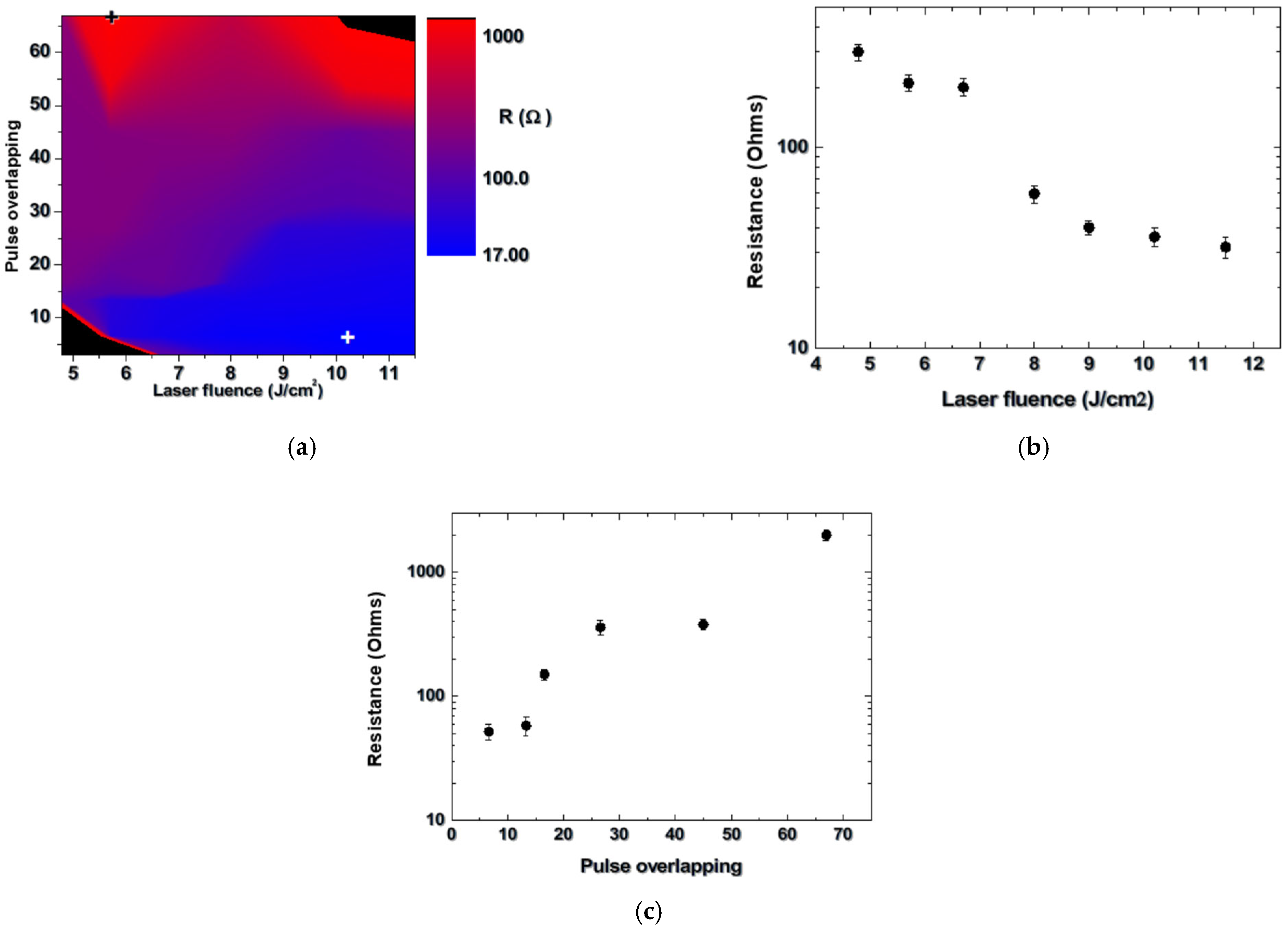
Figure 2a shows a dependence of the resistance value of formed tracks on the surface of AlN ceramic on the applied laser fluence and pulse overlapping.
For the presented conditions, a variation of R from 17 to about 2000 Ohms is observed. The areas in black show conditions where the resistance value is higher than the maximal one that can be measured with the available measuring system, which is 2 GOhms. The white and black crosses mark the conditions where the minimal and the maximal values of the resistance are measured, i.e., 17 Ohms and 2000 Ohms, respectively. The former is obtained at a fluence of 10.2 J/cm
2 and pulse overlapping of 6. The highest value is obtained at a fluence of 5.7 J/cm
2 and pulse overlapping of 67. For a better quantitative presentation, two examples of the dependences of the resistance on the laser fluence at a fixed overlapping of 6 in
Figure 2b, and on the pulse overlapping at a fixed fluence of 5.7 J/cm
2 in
Figure 2c, are also shown.
The presented data indicate that the pulse overlapping of only a few pulses is sufficient for fabrication of a track with resistance in the range of tens of Ohms. This is important since it expresses the ability of fast-track fabrication, i.e., the use of a high translation speed. At low pulse overlapping and low fluence, the decomposition of the nitride ceramic is not efficient and the formed structures are not conductive. Such structures are also produced when the pulse overlapping is in the range of a few tens, especially at the highest fluences used. Note that an experiment conducted in air indicates that at a fluence of 10.2 J/cm2 and pulse overlapping of 6, the track resistance is 130 Ohms, about 8 times higher.
The conductivity of the fabricated structures is related to the formation of aluminum on the surface of the ceramic. The decomposition of the AlN is thermally induced as the low-required energy reaction leads to the ejection of nitrogen and remaining aluminum, usually in liquid phase [
15,
19]. The performed XRD analysis confirms the formation of Al.
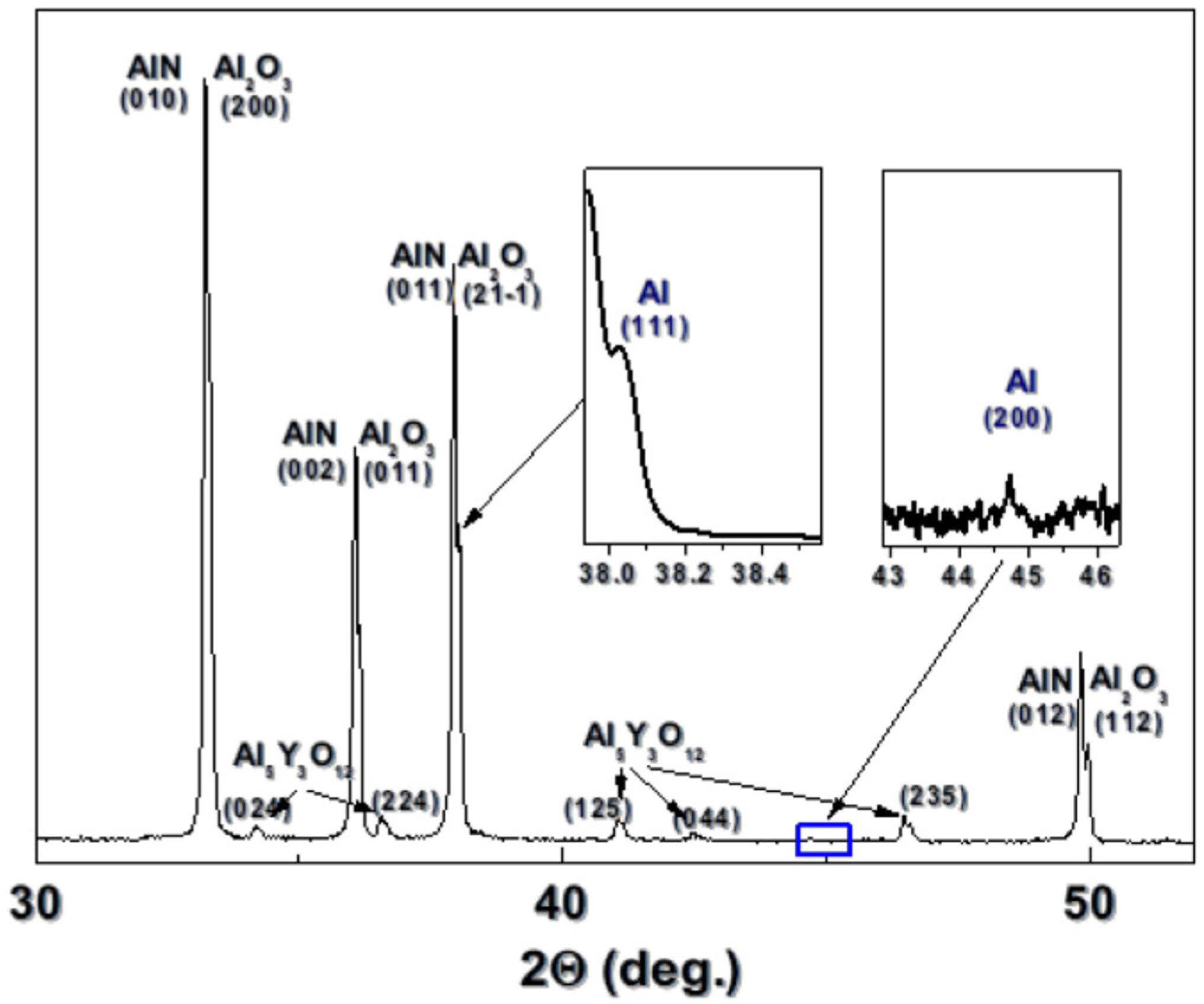
Figure 3 shows the XDR spectrum of a structure fabricated at a laser fluence of 10.2 J/cm
2 and pulse overlapping of 6, in vacuum. The analyzed area consists of AlN (98-060-8626), Al
2O
3 (98-016-9722), Al (98-0169722), and Al
5Y
3O
12 (98-077-4607).
The presence of the yttrium-composed phase is related to the inclusion of Y
2O
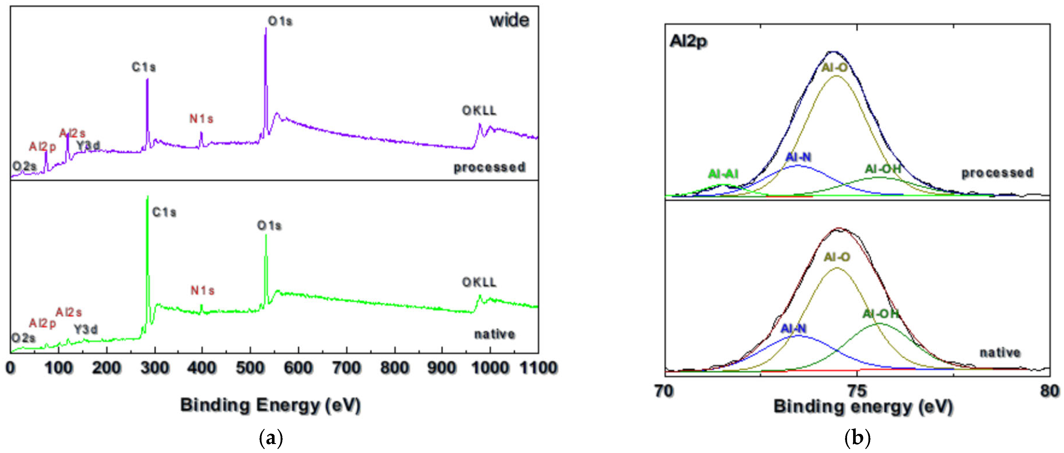
3 in the preparation stage of the ceramic, which improves the material stability and formation component. Further clarification of the material composition in the processed area is given by XPS analysis. In
Figure 4, wide spectra and Al2p spectra, and their corresponding convolution components for native and laser processed surfaces, are shown. The processing is performed under the same conditions as in
Figure 3. The spectra indicate that the surface of the material before and after irradiation is dominated by an oxide phase, and after laser irradiation, metallic aluminum is formed. The surfaces also contain -OH compounds. The wide spectra also show a decrease in the presence of nitrogen (with respect to Al peak intensity), which confirms the realization of the decomposition reaction.
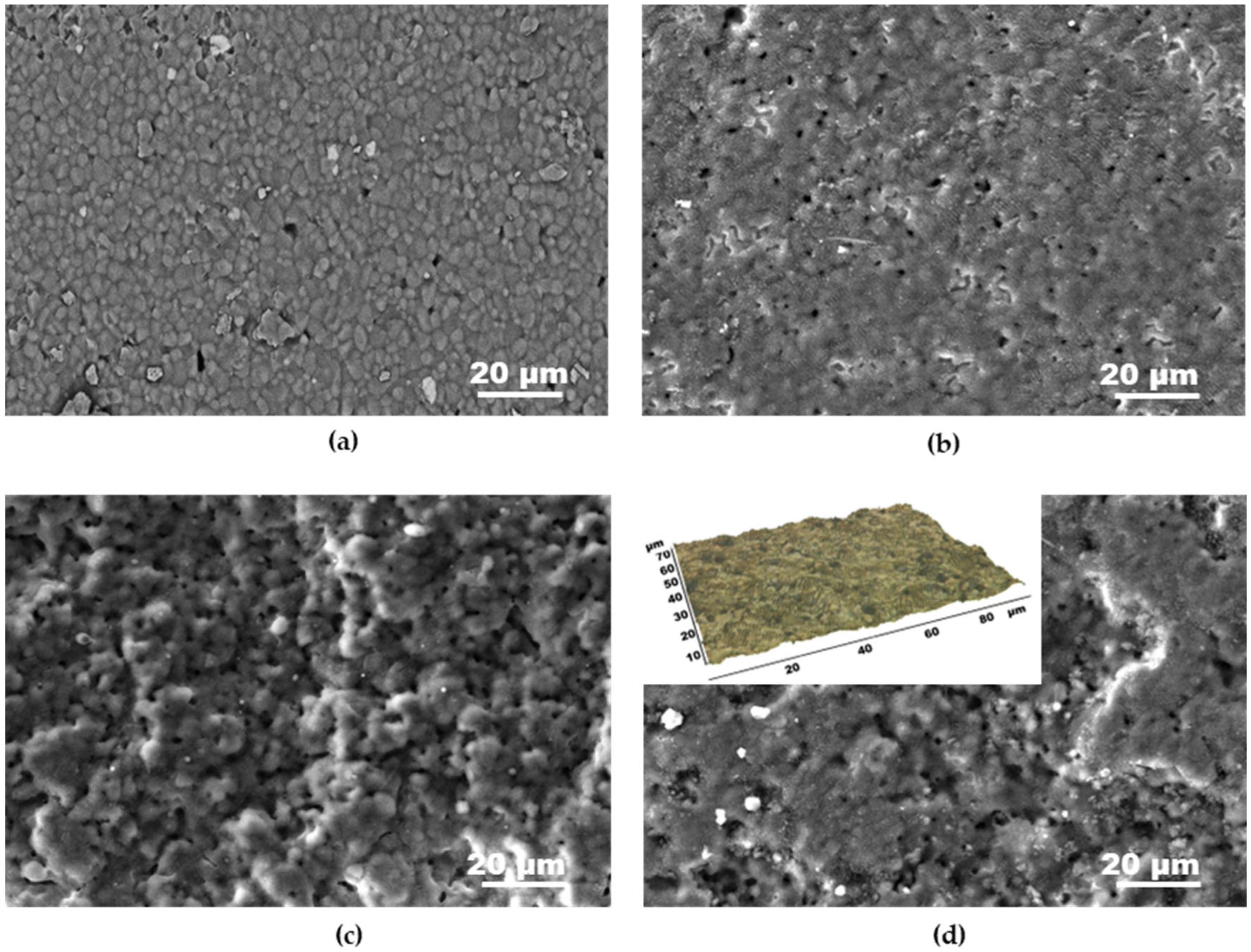
The morphology characterization of the laser-processed areas reveals modifications of the surface compared to the native ceramic, as the relief characteristics depend on the experimental conditions.
Figure 5 represents SEM images of the surface of AlN ceramic after treatment at different laser fluences and pulse overlapping. The native ceramic surface (
Figure 5a) expresses a morphology defined by the AlN crystallites that compose the material. After the laser processing at the presented conditions, this morphology is not present and the ceramic surface seems covered by a thin melt layer. According to the performed analyses, it can be concluded that it is the conductive aluminum film formed after the laser-induced ceramic decomposition. Under the experimental conditions where the minimal resistance is obtained in this work (laser fluence of 10.2 J/cm
2 and pulse overlapping of 6), the ceramic surface seems the smoothest one (
Figure 5b). With the decrease in laser fluence to 5.7 Jcm
2 and at the same overlapping, the surface morphology is characterized by the presence of a higher density of irregularities (
Figure 5c).
Under these conditions, the resistance of the track is about 3 times higher compared to the minimal one, reaching a value of 52 Ohms.
Figure 5d presents the morphology of the surface fabricated at a laser fluence of 10.2 J/cm
2 and pulse overlapping of 67. The image reveals the formation of well-expressed micrometer irregularities with abrupt walls. The structure with this morphology is not conductive. These results indicate that the increase in the pulse overlapping may lead to ablation of big portions of material, which induces an interruption of the surface film discontinuity and leads to the formation of electrically nonconductive material. For a better representation of the surface morphology, 3D analysis of the surfaces was performed using an optical profilometer. An example of the obtained images in shown in
Figure 5d. The analysis also gives the quantitative characterization of the surface roughness, as the obtained values for the average roughness (Ra) for the cases presented in
Figure 5 are 0.5, 0.56, 2.56, and 3.8 µm for
Figure 5a–d, respectively. It is found that the observed increase in the material resistance corresponds to the increase in the surface roughness expressed by Ra values.
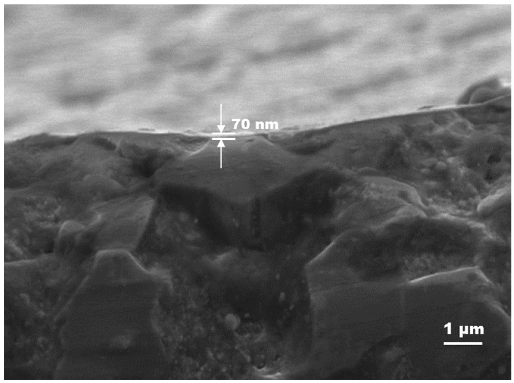
Using cross-sectional SEM imaging, the approximate thickness of the formed film on the ceramic surface could be estimated.
Figure 6 shows an image for the material fabricated at the laser fluence of 10.2 J/cm
2 and pulse overlapping of 6, where the track resistance is minimal. The sample for measurement was obtained by the breakage of the ceramic. Such an analysis indicates a thickness of the film of about 70 nm.
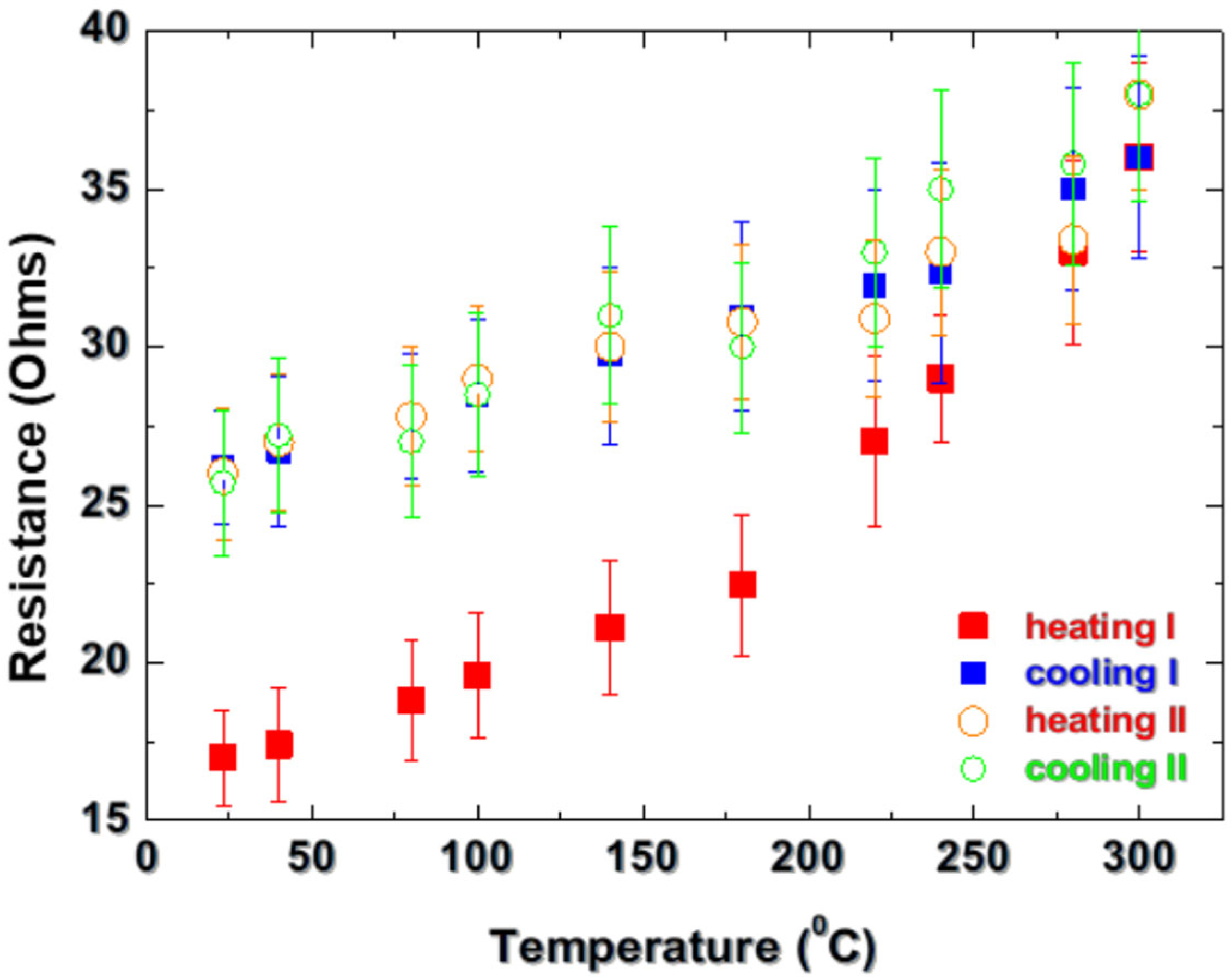
The further characterization of the fabricated conductive tracks includes an analysis of their thermal stability. Considering a potential use as heating element or operation at a higher temperature, this characteristic is crucial, since it will show the range of structure applicability. The first test is a “passive” one, where a conductive structure is heated by a heater and the resistance value is measured. The resistance measurement is also conducted in the cooling stage.
Figure 7 represents the dependences for the structure obtained at a fluence of 10.2 J/cm
2 and pulse overlapping of 6. Two consecutive tests were conducted, namely heating to a temperature of 300 °C (heating I), then cooling to room temperature (cooling I), and then performing the procedure again (heating II and cooling II). The maximal heating temperature is considered based on the fact that the oxidation of aluminum at temperatures lower than approximately 270 °C leads to the formation of an oxide layer with a thickness of about 2 nm, which is stable and prevents the metal from undergoing deeper oxidation [
25]. Thus, in this temperature range the oxidation is expected to make a weak contribution to the track performance. The experiments indicate that the formed structure remains conductive for the used range. In the first heating experiment, the resistance increases with the temperature, as is expected for a metal. At temperatures of about 180 °C, a steeper dependence is observed (red squares). At a temperature of 300 °C, the resistance value reaches 36 Ohms. In the cooling stage, the resistance decreases more homogeneously as the steeper dependence is not observed (blue squares). The resistance value in all of the range remains higher than that for the heating stage, as at room temperature its value is 26 Ohms. The second run of heating (red circles) starts at this resistance value. In this case, a steeper increase in the resistance is not observed in the investigated temperature range. The resistance increases following a dependence that can be described well by a linear fit. In the cooling stage (blue circles), the resistance values are close to those in heating stage II for the corresponding temperature, with a maximal variation of about 10%.
The presented behavior is an indication that in the first heating run a permanent change in the conductive material takes place. This could be related to aluminum layer morphology changes at micro- and nanoscales and/or an increase in the amount of the oxide phase. These changes, however, are permanent and lead to a stabilization of the structure, which results in a reversible behavior of the resistance with the temperature when repeating the experiment.
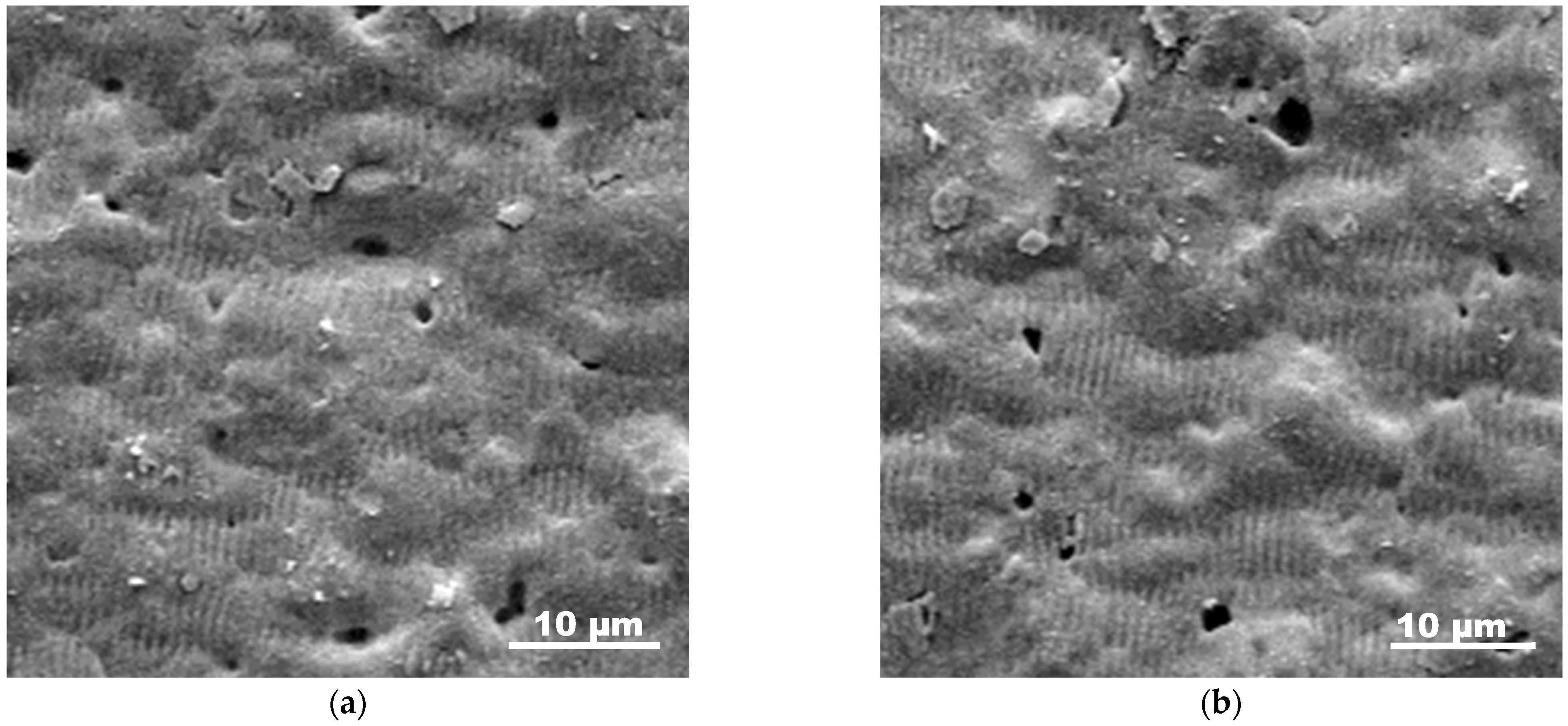
Figure 8 represents SEM images of areas in a track fabricated at a fluence of 10.2 J/cm
2 and pulse overlapping of 6, before (
Figure 8a) and after (
Figure 8b) the first run of heating and cooling. The structures express a characteristic ripple structure, which has been already reported for laser processing of AlN [
26].
The presence of such a structure benefits analysis of the realization of phase changes as melting of the surface when such ripples could not be preserved. As seen in
Figure 8, the surface morphology is preserved after heating, which is an indication that melting of the surface layer is not realized and the surface characteristics are stable after heating to 300 °C. Furthermore, application of macroscopic methods such as XPS and EDX does not show a clear change in the oxide phase. However, it should be considered that since the ceramic surface is rough, as can be seen in the SEM images, the conductive aluminum layer would have variation in its thickness. Since the melting or surface modification temperature of a thin film may depend on the thickness [
27,
28], it can be considered that some micro- or nanosized local changes could be realized, influencing the resistance. Since the steep increase in the resistance is not observed in the second heating experiment, it can be considered that these changes stabilize the morphology in terms of preserving its conductivity. The effect related to oxidation also could be taken into consideration, since even a small absolute increase in the oxide layer thickness could be significant as a relative value. In this case, however, one could consider a passivation effect.
It should be noted that for annealing at temperatures below approximately 150 °C, a steep increase in the structure resistance is not observed, and in the cooling stage the resistance values correspond to these in the heating stage at the given temperature, i.e., such a temperature does not cause a permanent modification of the material. Using the dependence as shown in
Figure 7, one can estimate the temperature coefficient of resistance α from the relation of the change in the resistance, R, with the temperature change ΔT, R = R
0 (1 + αΔT) [
29]. An estimation using the dependence presented in
Figure 7 for heating II gives a value of 1.4 × 10
−3 °C
−1, which is about 3 times lower than that for aluminum. This could be explained by the more complex composition of the formed conductive layer (the presence of AlN, Al
5Y
3O
12) and the observed decrease in α with the film thickness [
30].
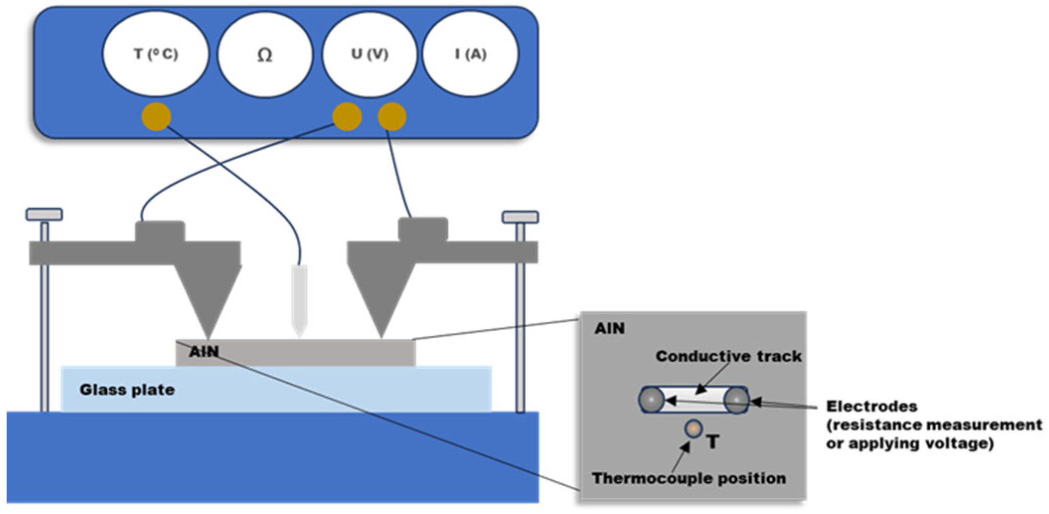
In the second type of experiments, the laser-fabricated structures were used as a heating element. For this purpose, DC voltage was applied between the two electrodes located at the two ends of the track (see
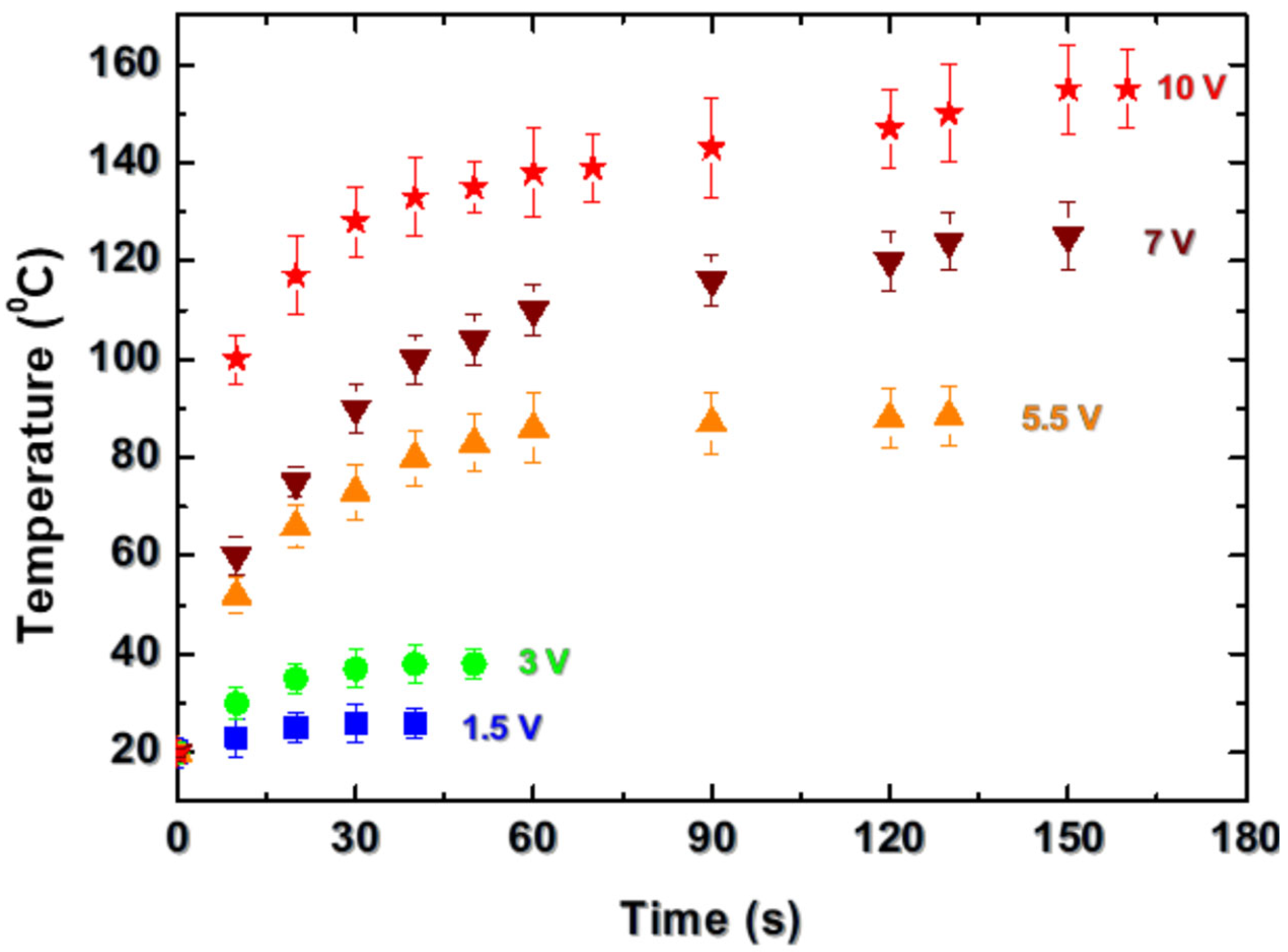
Figure 1).
Figure 9 shows the dependence of the temperature on the time when a different voltage was applied to an element obtained with a laser fluence of 10.2 J/cm
2 and pulse overlapping of 6. The sample was annealed to 300 °C under the conditions presented in
Figure 7 (first cycle). The dependencies are traced until the change in the temperature is about 1 °C per 10 s. The resistance value for the temperature range achieved at 10 V changes from 26 to about 28 Ohms, which defines an average current of about 370 mA through the track. The stability of the heater element is traced for a period of 2 h for the cases of application of 5.5 V and 10 V. In the first case, the element supports the temperature for the measuring time. This experiment was repeated three times, and the results for the achieved maximal temperature differ by less than 10%. In the case of operation at 10 V, the temperature is stable for a period of about 30 min then the resistance increases rapidly, with a jump of about an order of magnitude (230 Ohms), which results in a current drop. As a result, the maximal temperature decreases to about 50 °C and stays stable for the rest of the measuring time. Although the resistance value decreases in the cooling stage, it remains about an order of magnitude higher after the cooling of the sample to the room temperature. When the sample is cooled, it is found that a slight movement in the electrodes results in a return of the resistance value to the initial value of about 26 Ohms. This is an indication that a change in the material in the contact area between the electrodes and the structure could be responsible for the observed behavior while the rest of the material in the track preserves its properties. In the contact zone, the contact resistance could be higher due to the small contact area between the track having a high roughness, as seen in the SEM images, and the electrodes.
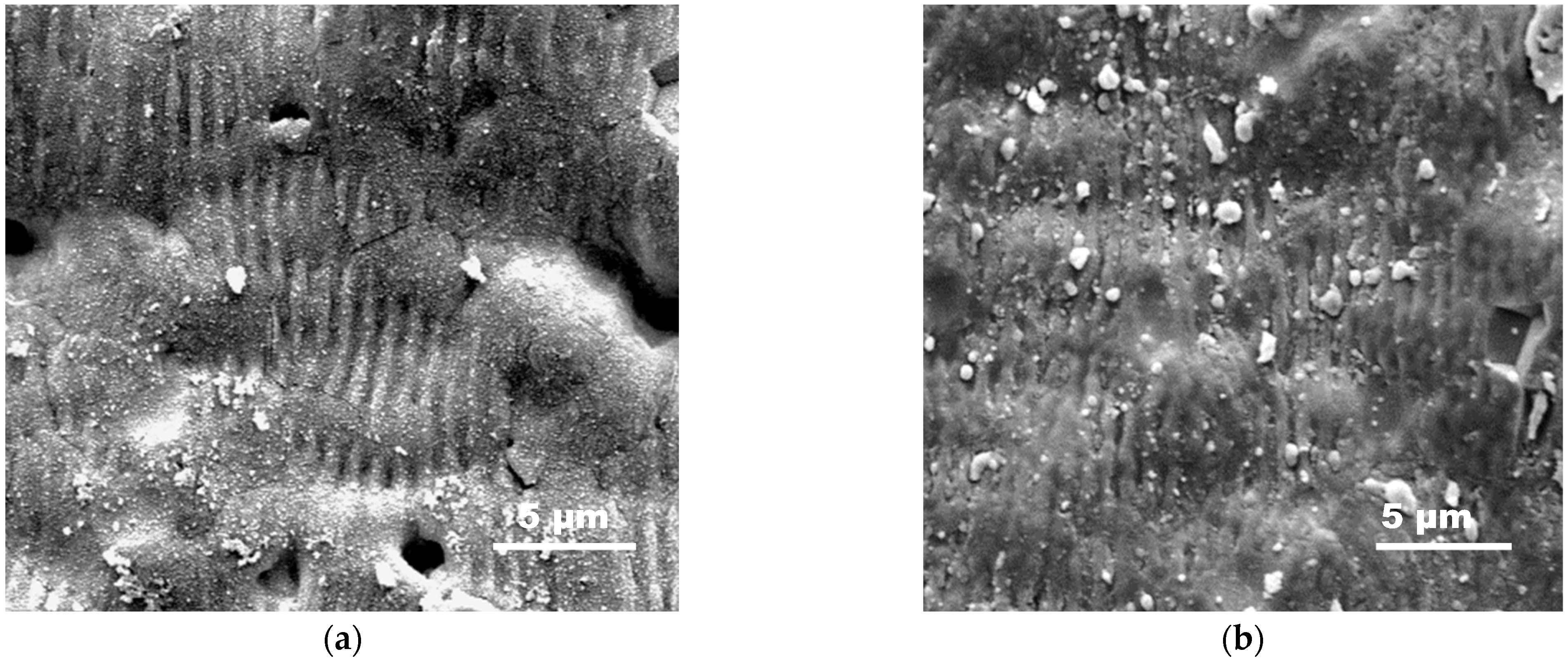
The increased contact resistance could induce local heating of the material, leading to enhanced oxidation and material modification, which may result in the conductivity being cut off, as the effect is more pronounced with the increase in the current. In order to clarify a change in the material, the morphology of the area of contact was examined.
Figure 10 shows SEM images of an area approximately in the middle of the processed area and in the zone of the contact between one of the electrodes and the track formed. The fabrication conditions are the same as in
Figure 9 and 10 V is applied on the sample. The areas of contact can be easily defined since they express a light brown color visible with the naked eye. A comparison of the images shows that in the contact area (
Figure 10b), the characteristic ripples are observed in fewer areas on the surface and they express smoother edges. The effect can be attributed to locally enhanced heating that induced melting or softening of the material, which blurs the crests’ borders and can be induced by a high contact resistance. Furthermore, EDX analysis indicates an increase in the presence of oxygen of about 12% in the contact zone, compared to the middle of the track. Thus, an increase in the oxide layer in the zone is realized.
Based on the results obtained, it can be concluded that, under the presented conditions and experimental setup, the laser-induced tracks in AlN ceramic can be used as an integrated heating element that can be used reproducibly to a maximal temperature of about 90 °C (current of about 200 mA). The heater performance could be improved by engineering solutions to achieve better connection of the electrodes, for example, by soldering or other bonding technologies. Furthermore, encapsulation of the structure to prevent oxidation could enable a use for higher temperatures. The main benefits of the demonstrated structures are easy fabrication of the conductive tracks; excellent integration into the ceramic, which is a material with high thermal conductivity, allowing fast spreading of heat in a large area; and the ability to fabricate small heating elements and those with a more complex shape defined by laser scanning on the desired geometry. Furthermore, the proposed method of laser-induced conductive track formation could offer some advantages compared to commercial technologies such as printing. In laser technology, no additional material such as ink is needed and the adhesion of the formed material is very good. In fact, there is no clear border between the formed aluminum layer and the ceramic, but the transition is smooth. This makes the conductive layer very stable, even for mechanical interaction. The laser method offers a change in the track resistance in a broad range by changing the processing parameters. This could be useful for the design of heaters with a small size or an electric circuit that includes AlN ceramic. In addition, the fabrication method does not require initial preparation of the ceramics surface. The conductive structures on ceramic can be formed on the ceramic as it is delivered by the producer. The reason for this is that the laser processing removes the surface layer. Since the laser radiation can be focused at a spot with a size less than the used wavelength, even sub-micrometer tracks could be fabricated. This increases the spatial resolution of the method. Furthermore, if for any reason the conductive track is damaged, it can be easily re-fabricated by the same process on the same place.


 ,
, 