Article

Highly Stable, Flexible, Transparent Hybrid Strontium Titanate Conductive Thin Films with Embedded Cu Nanowires

by
Ming Liu
1,
Shihui Yu
2,*,
Lijun Song
2,
Jiesong Li
3 and
Jian Feng
4
1
School of Materials Science and Engineering, Luoyang Institute of Science and Technology, Luoyang 471023, China
2
School of Power Electrical Engineering, Luoyang Institute of Science and Technology, Luoyang 471023, China
3
Triumph Information Display Materials (Luoyang) Co., Ltd., Luoyang 471023, China
4
Luobo Group Luoyang Longhai Electronic Glass Co., Ltd., Luoyang 471023, China
*
Author to whom correspondence should be addressed.
Materials 2025, 18(10), 2398; https://doi.org/10.3390/ma18102398
Submission received: 11 April 2025 / Revised: 16 May 2025 / Accepted: 20 May 2025 / Published: 21 May 2025
(This article belongs to the Section Thin Films and Interfaces)

Abstract

:
To meet the stringent demands of next-generation flexible optoelectronic devices, a novel fabrication approach is employed that integrates the spray-coating of copper nanowires (Cu NWs) with the magnetron sputtering of SrTiO3 thin films, thereby yielding SrTiO3/Cu NWs/SrTiO3 hybrid thin films. The incorporation of the SrTiO3 layers results in improved optical performance, with the transmittance of the Cu NW network increasing from 83.5% to 84.2% and a concurrent reduction in sheet resistance from 16.9 Ω/sq to 14.5 Ω/sq. Moreover, after subjecting the hybrid thin films to 100 repeated tape-peeling tests and 2000 bending cycles with a bending radius of 5.0 mm, the resistance remains essentially unchanged, which underscores the films’ exceptional mechanical flexibility and robust adhesion. Additionally, the hybrid thin films are subjected to rigorous high-temperature, high-humidity, and oxidative conditions, where the resistance exhibits outstanding stability. These results substantiate the potential of the SrTiO3/Cu NWs/SrTiO3 hybrid thin films for integration into flexible and wearable electronic devices, delivering enhanced optoelectronic performance and long-term reliability under demanding conditions.

1. Introduction

Flexible transparent conductive thin films (TCFs) are the essential components in modern electronics, finding applications in devices such as organic light-emitting diodes, touch screens, wearable sensors, solar cells, and transparent heaters [1,2,3,4,5]. Indium tin oxide (ITO) is widely employed in TCFs due to the exceptional optical transmittance and low sheet resistance [6,7]. However, ITO faces significant challenges in flexible electronics because of the high cost and limited availability of indium, as well as the inherent brittleness [8]. Consequently, there is growing interest in exploring alternative materials to replace ITO [9,10,11]. Metallic nanowires (NWs) have emerged as a promising candidate due to their excellent electrical conductivity, mechanical flexibility, and transparency [12,13,14,15]. Although gold and silver NWs deliver outstanding performance, their high cost precludes their practical application. In contrast, Cu NWs have attracted considerable attention due to their low cost [15,16]. However, the high susceptibility to oxidation when exposed to ambient conditions undermines the long-term durability [17]. Moreover, when Cu NWs are deposited directly onto polymer substrates, the poor adhesion often leads to detachment, bending, or peeling [18]. These drawbacks significantly impede the widespread adoption of Cu NWs in flexible TCFs.
A number of approaches have been investigated to enhance the oxidation resistance of Cu NWs [19,20]. Passivation layers composed of highly stable metals such as Au [21], Pt [22], Ni [23], and Ag [24] have been studied. However, controlling the precise thickness of these metallic coatings remains difficult, often resulting in diminished optical transmittance and failing to address the inherent adhesion challenges of Cu NWs. Another commonly explored strategy is the deposition of graphene layers onto Cu NW networks to serve as a protective barrier. Nevertheless, the intrinsic defects present in thin graphene coatings offer inadequate protection, and while thicker graphene layers can improve stability, they concurrently cause a significant reduction in optical transmittance [25]. In contrast, several metal oxides—including Al-doped ZnO [26], Sb-doped SnO2 [27], Al2O3 [28], and TiO2 [29]—have been reported to effectively mitigate the oxidation of Cu NWs. These oxide coatings not only enhance the durability and adhesion of Cu NW networks but also maintain the optical and electrical performance of the thin films, rendering them a more promising solution for improving the overall stability of Cu NW-based transparent conductive films.
Strontium titanate (SrTiO3), as a typical perovskite-type wide-bandgap semiconductor material (with a room-temperature bandgap of approximately 3.2 eV) [30], has demonstrated significant application value in photodetectors, capacitor dielectric layers, and photocatalytic materials due to its superior optical transmittance (>80% in the visible-light region) and unique dielectric properties [30,31]. However, research on the composite design of strontium titanate thin films with copper nanowires (Cu NWs) to achieve synergistic enhancement in optoelectronic properties through interface engineering remains unexplored in the literature. In this study, flexible transparent conductive thin films composed of the SrTiO3 and Cu NWs are fabricated via RF magnetron sputtering combined with spray-coating. The pristine Cu NW networks exhibit a sheet resistance of 16.9 Ω/sq at a transmittance of 83.5%. After the combination of SrTiO3 thin films, the sheet resistance is decreased to 14.5 Ω/sq, while the transmittance is increased to 84.2%. Moreover, the SrTiO3/Cu NWs/SrTiO3 hybrid thin films retain the mechanical flexibility and resistance stability under high temperature, high humidity, and severe oxidation.

2. Materials and Methods
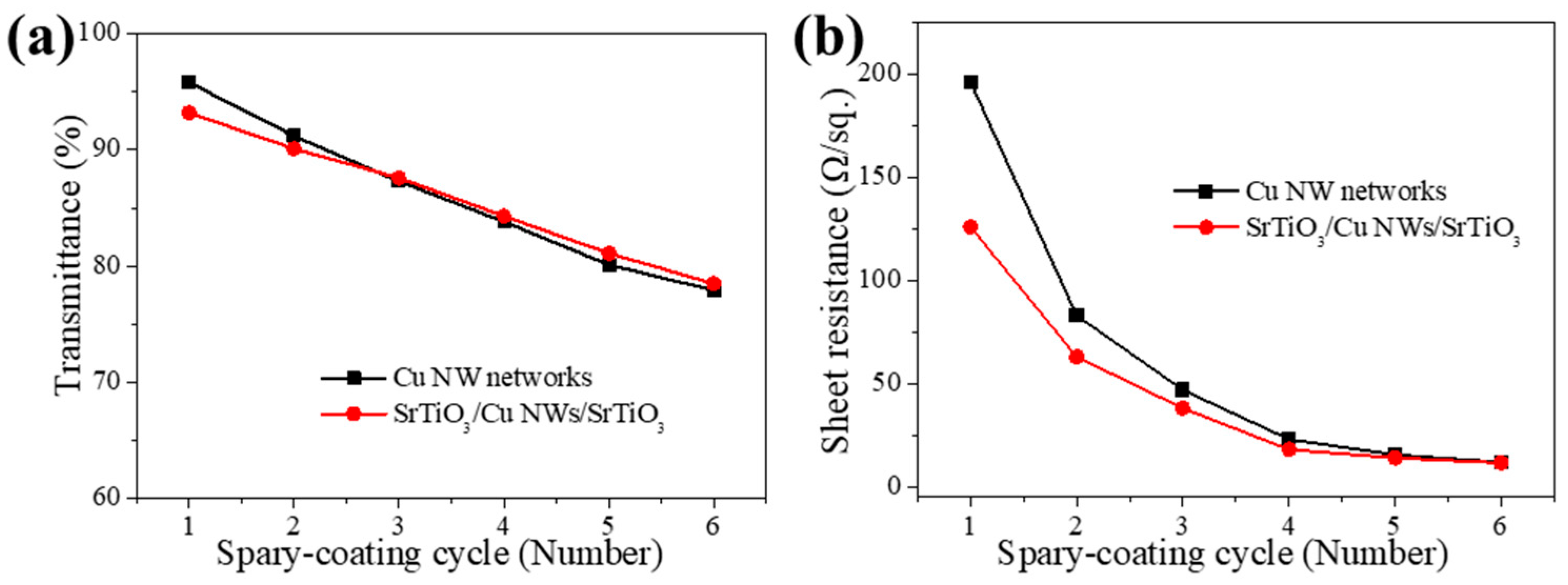
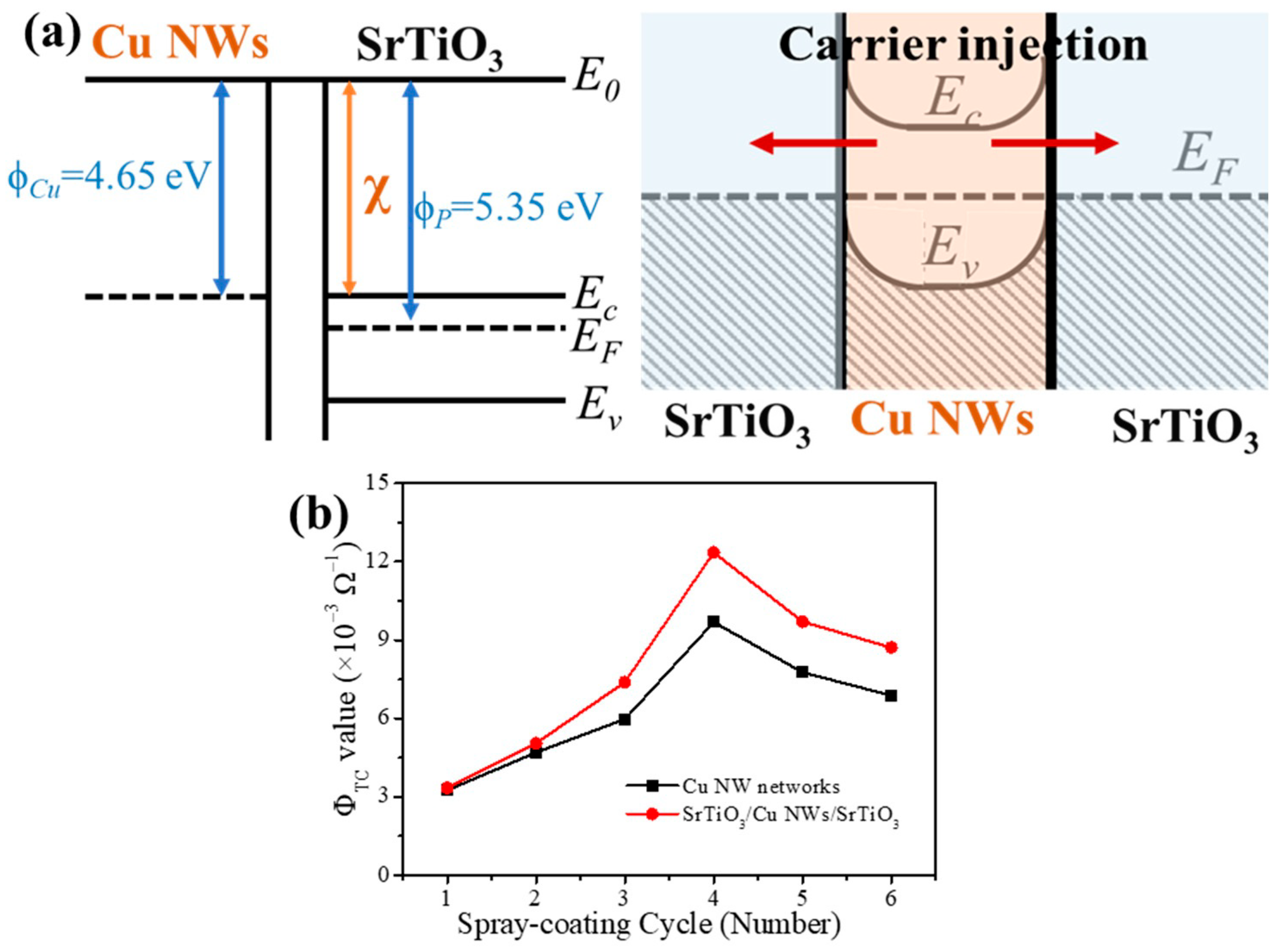
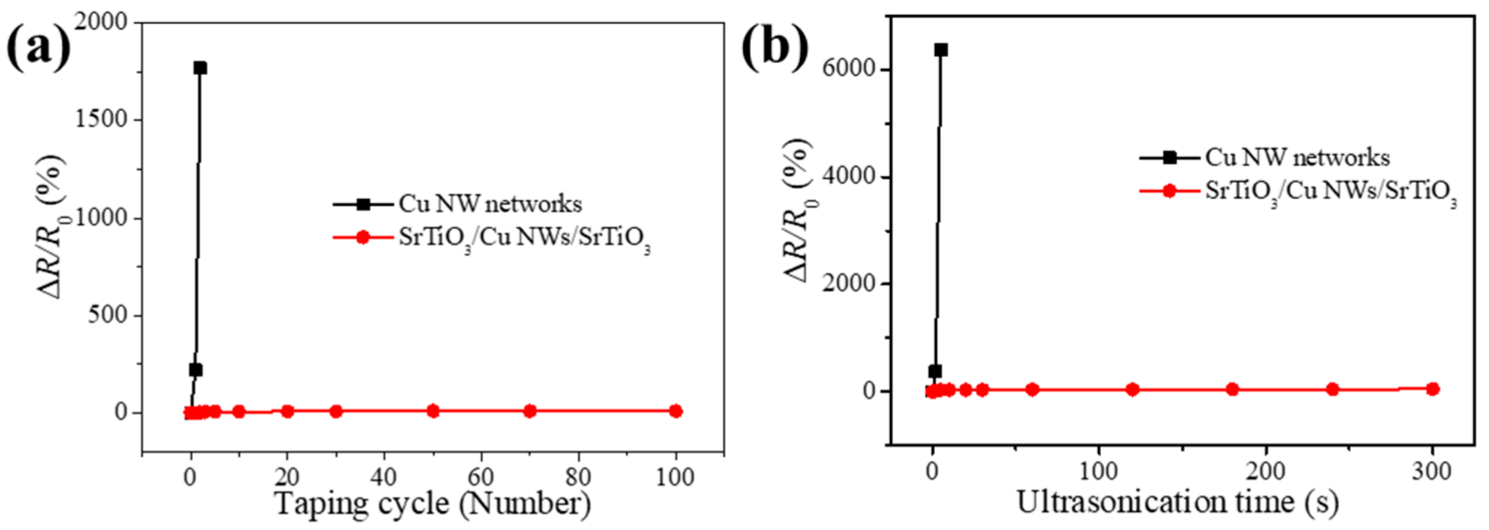
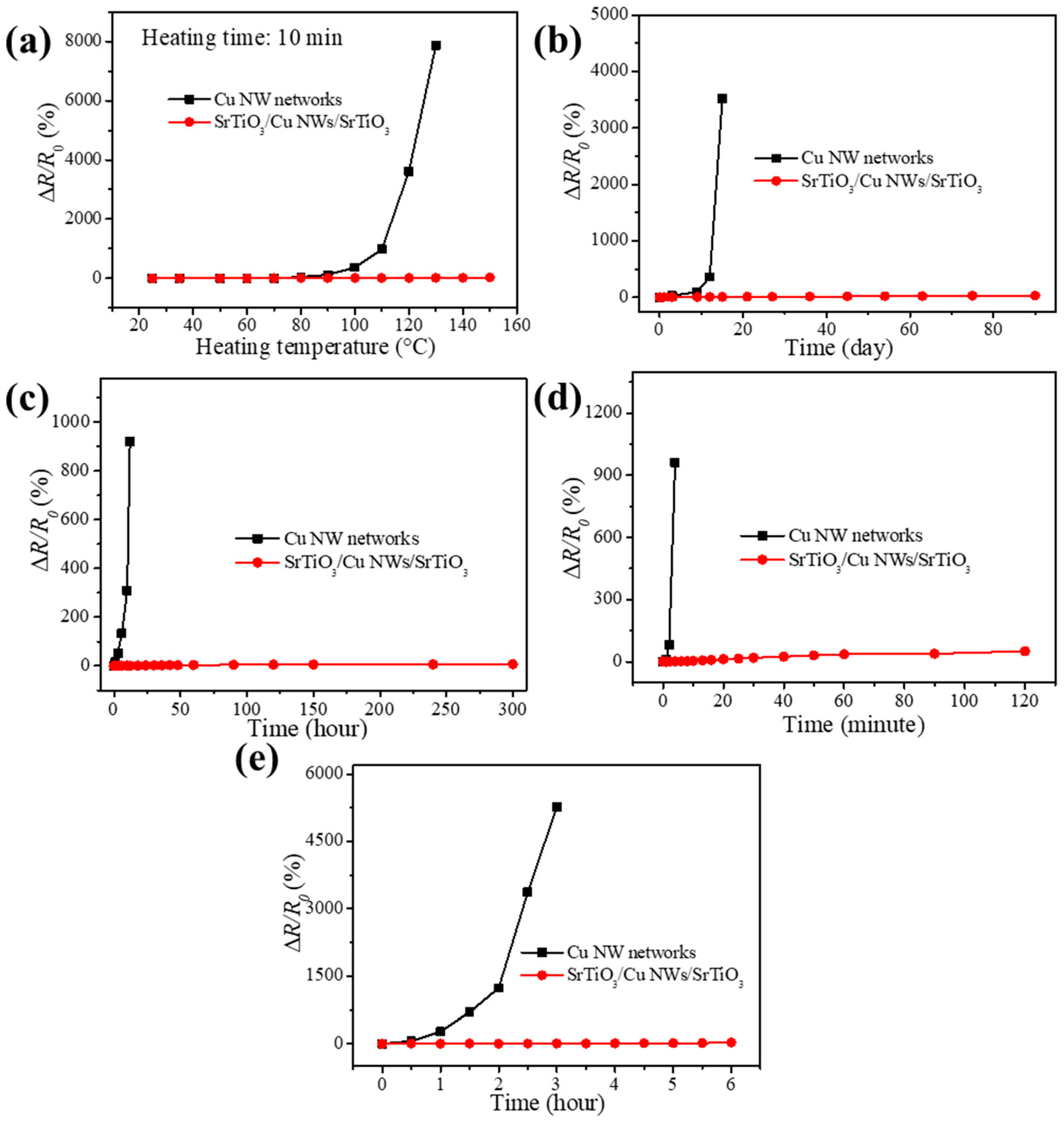
SrTiO3/Cu NWs/SrTiO3 hybrid thin films were deposited onto transparent polyethylene terephthalate (PET) substrates via a combined RF sputtering and spray-coating approach. In this process, both the top and bottom SrTiO3 layers—each 50 nm thick—were fabricated using SrTiO3 ceramic targets of 99.99% purity. The ceramic targets, with dimensions of 50 mm in diameter and 5 mm in thickness, were sputtered in an environment of 99.999% high-purity argon at a controlled pressure of 1.0 Pa and a sputtering power of 60 W, while the substrate temperature was maintained at room temperature throughout deposition. Subsequently, an optimized spray-coating technique was employed to uniformly deposit the Cu NW solution onto the PET substrate, ensuring consistent coverage. The spraying duration was 5 s. After drying at 60 °C, the next coat was applied. The process was repeated one to six times. The coated substrate then underwent an acid leaching treatment using a 70% acid solution for one minute, effectively removing residual organic contaminants from the film surface. Finally, the Cu NW networks were carefully extracted from the solution and dried under a stream of nitrogen gas, thereby ensuring complete moisture removal and promoting film stabilization.
The film structure was characterized using a D/MAX-RB X-ray diffraction instrument (XRD, Rigaku, Japan). The surface morphology was examined with a field emission scanning electron microscope (FE-SEM JSM-7001F, JEOL, Japan) and atomic force microscopy (AFM, Bruker Multimode 8, USA). Electrical properties were measured using an SX1934 four-probe resistance tester (BAISHEN, Suzhou, China), and optical properties were determined via a Varian Cary 5000 ultraviolet–visible–near-infrared spectrometer (Agilent, USA). Additionally, the film’s flexibility was evaluated using a Nanoupe+ flexible tester (NANOUP ELECTRONICS, Changsha, China).

3. Discussion

Figure 1a presents a schematic structure of the SrTiO3/Cu NWs/SrTiO3 hybrid thin films deposited on PET substrates. In this configuration, the Cu NW network is encapsulated between two sputtered SrTiO3 layers, with the sheet resistance and transmittance being strongly dependent on the Cu NW density. The nanowire density is controlled by varying the number of spray-coating cycles used to deposit the Cu NW dispersion at a fixed concentration. The SrTiO3 thin films serve to encapsulate the Cu NWs effectively, thereby substantially improving their stability. Notably, these SrTiO3 thin films exhibit strong adhesion to the PET substrate [32], which further reinforces the attachment of the Cu NW network and ensures the composite maintains its structural integrity during subsequent processing and application. Figure 1b displays the XRD patterns of the SrTiO3/Cu NWs/SrTiO3 hybrid thin films, revealing two prominent diffraction peaks at approximately 43.2° and 50.1°. These peaks correspond to the (1 1 1) and (2 0 0) planes of pure face-centered cubic copper, with the Cu NWs demonstrating a preferential orientation along the (1 1 1) plane [33]. No characteristic diffraction peaks for SrTiO3 are detected, because the films, deposited at room temperature, remain amorphous; the crystallization of SrTiO3 typically requires temperatures above 500 °C [34]. The inset of Figure 1b shows an AFM image of the SrTiO3/Cu NWs/SrTiO3 hybrid thin film. The Cu nanowires are evenly distributed, but their interwoven structure raises the film’s surface roughness to 123 nm. Figure 1c shows an FE-SEM image of the Cu NW networks. The nanowires are randomly interwoven and uniformly distributed, thereby forming a percolating network that underpins the film’s favorable optical and electrical properties. Figure 1d further reveals the surface morphology of the SrTiO3 thin films, where the Cu NW junctions appear more tightly connected, indicating enhanced inter-nanowire contact and improved mechanical robustness. Importantly, the overall distribution of the Cu NW network is preserved following the deposition of the top SrTiO3 thin films, suggesting that the sputtering process does not adversely alter the underlying nanowire architecture.
Figure 2a presents the optical transmittance measurements for both Cu NW networks and SrTiO3/Cu NWs/SrTiO3 hybrid thin films fabricated with varying numbers of spray-coating cycles. Following a single spray-coating cycle, both types of samples exhibit an optical transmittance of above 90%. With additional cycles, the Cu NW density increases, leading to a gradual decline in transmittance. After five cycles, the transmittance for both samples decreases to below 80%. At such high nanowire densities, the Cu NW networks become sufficiently dense and thick, effectively acting as a reflective mirror. This observation underscores the importance of precisely controlling the Cu NW density to optimize the optical properties of SrTiO3/Cu NWs/SrTiO3 hybrid thin films when they are employed as top window electrodes. Notably, under identical spray-coating conditions, the SrTiO3/Cu NWs/SrTiO3 hybrid thin films demonstrate a slightly higher transmittance compared to the pristine Cu NW networks. This improvement stems from the SrTiO3 layer, which tightens the junctions between the Cu nanowires, smooths the film surface, and therefore reduces optical scattering.
Figure 2b depicts the evolution of sheet resistance as a function of spray-coating cycles for the samples. With increasing spray-coating cycles, the enhanced density of the Cu NW networks leads to the formation of additional electron transport pathways, thereby progressively reducing the sheet resistance [28]. Moreover, the incorporation of SrTiO3 thin films contributes to a further modest decrease in sheet resistance. As evidenced in Figure 1d, the deposition of SrTiO3 induces tighter interconnections at the junctions between individual Cu NWs, likely due to the impact of SrTiO3 particles during the deposition process, which in turn improves the contact between the nanowires and reduces inter-junction resistance [35]. Consequently, the overall sheet resistance of the SrTiO3/Cu NWs/SrTiO3 hybrid thin films is lower compared to that of the bare Cu NW networks.
The work functions of SrTiO3 and Cu NWs are 5.35 eV [36] and 4.65 eV [37], respectively. Due to the n-type nature and higher work function of SrTiO3 thin films, an ohmic contact is formed when SrTiO3 is interfaced with Cu NWs [38]. Figure 3a depicts the schematic band diagram for the SrTiO3/Cu NW interface. Upon contact, a potential barrier exists that drives a significant flow of free electrons from the Cu NWs into the SrTiO3. This electron transfer leads to the formation of a negative space charge region near the interface in SrTiO3, which in turn establishes a built-in electric field directed from SrTiO3 towards the Cu NWs. Concurrently, the conduction band of SrTiO3 bends downward while its valence band curves upward, reinforcing the n-type characteristic at the interface. Once thermodynamic equilibrium is achieved, the Fermi levels align across the interface, effectively reducing the potential barrier to zero and facilitating electron injection from the Cu NWs into the SrTiO3 thin films. This enhanced electron injection increases the overall carrier concentration and thereby reduces the sheet resistance in the SrTiO3/Cu NWs/SrTiO3 hybrid thin films.
For practical applications, transparent conductive films must exhibit both low sheet resistance and high light transmittance to allow maximum incident light to reach the absorber layer [39]. To optimize the optoelectronic performance of the SrTiO3/Cu NWs/SrTiO3 hybrid thin films, we evaluated the figure of merit (ΦTC) as defined by Haacke, which is calculated using the sheet resistance (Rs) and transmittance (T) according to the following equation [40,41]:
Φ T C = T 10 R s
Figure 3b shows the variation in the calculated ΦTC value for the Cu NW networks and SrTiO3/Cu NWs/SrTiO3 hybrid thin films with different spray-coating cycles. The ΦTC value increases with the number of spray-coating cycles, reaching a maximum value when the spray-coating cycle is 4. Specifically, the optimum ΦTC value of 12.35 × 10⁻³ Ω−1 is achieved at four spray-coating cycles, where the transmittance is 84.2% and the sheet resistance is 14.5 Ω/sq. Although a higher density of Cu NWs leads to a lower sheet resistance, further increasing the nanowire density beyond a critical threshold results in a significant reduction in optical transmittance, which in turn lowers the ΦTC value. Thus, the SrTiO3/Cu NWs/SrTiO3 hybrid thin films produced with four spray-coating cycles offer an optimal balance, ensuring enhanced light transmission in the visible range while maintaining high electrical conductivity.
Figure 4a presents the bending test results for the ITO on PET, SrTiO3/Cu NWs/SrTiO3 hybrid thin films, and the Cu NW networks. The variation in resistance is defined as ΔR = (RR0), where R and R0 represent the post-bending and initial resistance, respectively. When the bending radius is reduced from 30 mm to 5 mm, the resistance of flexible ITO thin films increases dramatically by a factor of 7.7, due to the formation of cracks caused by internal stresses arising during bending. The resistance of the SrTiO3/Cu NWs/SrTiO3 hybrid thin films increases by only 5%, whereas the untreated Cu NW network exhibits a 23% increase. This suggests that the SrTiO3 layers serve as an effective protective coating for the Cu NW network, stabilizing the conductive pathways by mitigating the geometric slippage at the nanowire junctions. Considering that film flexibility is inversely related to thickness [42], the ultrathin SrTiO3 layers further contribute to maintaining the overall flexibility of the hybrid structure. Figure 4b illustrates the bending fatigue characteristics for the ITO on PET, SrTiO3/Cu NWs/SrTiO3 hybrid thin films and the Cu NW networks under a constant bending radius of 5.0 mm. After 10 bending cycles, the resistance of the SrTiO3/Cu NWs/SrTiO3 hybrid thin films increases modestly by 9% and then remains nearly constant with additional cycles, whereas the bare Cu NW network’s resistance increases by 168% after 2000 cycles. The pronounced resistance escalation in the bare network is attributed to its loosely packed structure, where bending induces significant changes at the contact junctions, leading to progressive degradation of the conductive network. In contrast, embedding the Cu NWs within the SrTiO3 thin films results in reinforced inter-nanowire connections, which not only minimizes initial damage due to slight nanowire breakage during the first few cycles but also stabilizes the overall resistance thereafter. These findings highlight the superior mechanical durability and adhesion of the SrTiO3/Cu NWs/SrTiO3 hybrid thin films, demonstrating their promising potential for application in flexible electronic devices where consistent electrical performance under mechanical deformation is essential.
Although Cu NW networks exhibit excellent conductivity and flexibility, the adhesion to substrates is poor, making them vulnerable to mechanical stresses such as tape stripping in practical applications, which severely compromises electrode stability [43,44]. To address this concern, we compared the adhesion of SrTiO3/Cu NWs/SrTiO3 hybrid thin films with that of bare Cu NW networks using 3M 610 tape tests (3M Company, USA). As shown in Figure 5a, the bare Cu NW networks lose electrical conductivity after only two tape peeling cycles, indicating that the adhesion to the PET substrate relies solely on weak van der Waals forces and is easily disrupted [45]. In contrast, the SrTiO3/Cu NWs/SrTiO3 hybrid thin films maintain stable resistance even after 100 tape peeling cycles, demonstrating that the SrTiO3 thin films effectively enhance the overall adhesion by embedding the Cu NWs within the thin film structure. This is because the Cu NWs are embedded between the top and bottom SrTiO3 thin films, and the SrTiO3 completely covers the Cu NW networks; thus, the SrTiO3/Cu NWs/SrTiO3 hybrid thin films show better adhesion than the pure Cu NW films. Figure 5b presents the variation in resistance of SrTiO3/Cu NWs/SrTiO3 hybrid thin films and the Cu NW networks under different ultrasonic treatment durations. The bare Cu NW networks experience a rapid increase in resistance, completely losing conductivity within one minute of ultrasonic exposure; conversely, the resistance of the hybrid thin films remains nearly unchanged under similar conditions. This indicates that the top SrTiO3 layers provide robust protection against ultrasonic-induced damage, effectively suppressing nanowire breakage and detachment. The addition of dense and uniform SrTiO3 protective layers not only significantly improves the adhesion between the Cu NWs and the substrate but also greatly enhances the stability and durability of the composite electrode in harsh environments, thereby offering a strong technical foundation for the practical application of such transparent conductive electrodes in flexible electronic devices.
The long-term stability of flexible TCFs is a critical performance parameter, particularly for applications in flexible electronic devices such as displays, wearable sensors, and thin-film solar cells that may operate in high-temperature environments [46,47]. To assess the temperature resistance of the SrTiO3/Cu NWs/SrTiO3 hybrid thin films, the samples are subjected to heating at various temperatures for a duration of 10 min, while the change in electrical resistance is continuously monitored. As illustrated in Figure 6a, at temperatures below 80 °C, both the bare Cu NW networks and the hybrid thin films maintained a constant resistance, indicating that the intrinsic electrical properties of the materials remain unaffected by thermal excitation within this range. However, when the temperature exceeds 80 °C, the resistance of the bare Cu NW networks escalates sharply, culminating in a complete loss of conductivity at 120 °C. This deterioration is primarily due to the accelerated oxidation of the Cu NWs at elevated temperatures [48], which results in the fracture of the nanowire structure and the subsequent disruption of the conductive network. In contrast, the SrTiO3/Cu NWs/SrTiO3 hybrid thin films exhibit remarkable thermal stability, with the resistance remaining virtually unchanged over the entire temperature range tested. This enhanced stability is attributed to the dense SrTiO3 thin films that effectively encapsulate the Cu NWs, thereby preventing the ingress of oxygen and moisture and mitigating oxidation. It should be noted that the maximum heating temperature is restricted to 150 °C due to the softening temperature of the PET substrates [49].
In addition to controlled heating tests, long-term environmental stability was evaluated by exposing the samples to ambient conditions over extended periods. As shown in Figure 6b, the bare Cu NW networks gradually undergo oxidation when exposed to atmospheric oxygen and water vapor, resulting in a progressive increase in resistance and eventual loss of conductivity after 15 days. Conversely, the SrTiO3/Cu NWs/SrTiO3 hybrid films retained their initial resistance even after 180 days of exposure, which substantiates the long-term protective effect provided by the SrTiO3 coatings. To further assess oxidation resistance under accelerated conditions, both the bare Cu NW networks and the SrTiO3/Cu NWs/SrTiO3 hybrid thin films are subjected to controlled tests in a high-temperature, high-humidity environment (85 °C and 85% relative humidity). Figure 6c displays the temporal evolution of resistance under these conditions. The bare Cu NW networks show a dramatic increase in resistance, ultimately losing conductivity after 18 h. This behavior is indicative of rapid oxidative degradation that compromises the nanowire structure. In comparison, the resistance of the SrTiO3/Cu NWs/SrTiO3 hybrid thin films increases by only a factor of two over the same period. The homogeneous and dense SrTiO3 layers function as an effective barrier, isolating the underlying Cu NWs from reactive atmospheric species. Furthermore, complementary experiments were conducted by immersing the samples in a 3 wt% H2O2 solution to simulate a chemically aggressive oxidizing environment. As depicted in Figure 6d, the resistance of the bare Cu NW networks increases sharply with immersion time, leading to a rapid deterioration of conductivity. Meanwhile, the hybrid thin films exhibit only minor resistance changes during the early stages of immersion, owing to the dense microstructure of the SrTiO3 layers that effectively impede the direct contact between the oxidizing solution and the Cu NWs. Although prolonged exposure eventually allows some H2O2 to permeate the SrTiO3 layers and initiate slow oxidation, the resultant increase in resistance remains modest compared to the bare Cu NW networks. Figure 6e shows the resistance change of the bare Cu NW and SrTiO3/Cu NWs/SrTiO3 hybrid thin films after ultraviolet ozone (UVO) irradiation. The resistance of bare Cu NWs loses the conductivity after 3 h because of the oxidation and decomposition of Cu NWs, while that of SrTiO3/Cu NWs/SrTiO3 hybrid thin films is only increased by only 26% because of the protection of SrTiO3 thin films.

4. Conclusions

This work presents the development of the high-performance flexible TCFs by using Cu NW-embedded SrTiO3 thin films. The conductivity of the SrTiO3/Cu NWs/SrTiO3 hybrid thin films is solely caused by the Cu NWs as the SrTiO3 is highly resistive. The improvement in adhesion and stability of hybrid thin films can be attributed to the effective covering of SrTiO3 on the Cu NW networks. Moreover, the incorporation of the SrTiO3 layers results in improved optical performance, with the transmittance of the Cu NW network increasing from 83.5% to 84.2% and a concurrent reduction in sheet resistance from 16.9 Ω/sq to 14.5 Ω/sq. Furthermore, when subjected to 2000 bending cycles at a curvature radius of 5.0 mm, the resistance of the hybrid thin films is increased by only 11%, thereby demonstrating exceptional mechanical flexibility. In addition, the hybrid thin films display excellent adhesion and oxidation resistance; their resistance remains unchanged even after prolonged storage in high-temperature and high-humidity environments. These outstanding properties are anticipated to facilitate the practical application and widespread adoption of SrTiO3/Cu NWs/SrTiO3 hybrid thin films in various flexible optoelectronic devices.

Author Contributions

M.L. and S.Y.: investigation, methodology, experimentation, and writing—original draft. L.S., J.L., and J.F.: data curation and experimentation. All authors have read and agreed to the published version of the manuscript.

Funding

This work is supported by the National Natural Science Foundation of China (Grant No. 52175525), Science and Technology Project of Henan Province (Grant Nos. 252102210250, 242102211084, 232102231053), Training Plan of Young Backbone Teachers in Colleges and Universities of Henan Province (2021GGJS164).

Institutional Review Board Statement

Not applicable.

Informed Consent Statement

Not applicable.

Data Availability Statement

The original contributions presented in this study are included in the article. Further inquiries can be directed at the corresponding author.

Conflicts of Interest

Author Jiesong Li was employed by the company Triumph Information Display Materials (Luoyang) Co., Ltd. Author Jian Feng was employed by the company Luobo Group Luoyang Longhai Electronic Glass Co., Ltd. The remaining authors declare that the research was conducted in the absence of any commercial or financial relationships that could be construed as a potential conflict of interest.

References

  1. Yao, F.; Li, W.; Sks, S.K.; Fukuhara, C.; Badhulika, S.; Kong, C.Y. Scalable one-step synthesis of reduced graphene oxide: Towards flexible transparent conductive films and active supercapacitor electrodes. Chem. Eng. J. 2024, 488, 150828. [Google Scholar] [CrossRef]
  2. Yu, S.; Song, L.; Wu, C.; Li, L. Enhanced conductivity and stability of Cu-embedded zinc tin oxide flexible transparent conductive thin films. Ceram. Inter. 2022, 48, 15925–15931. [Google Scholar] [CrossRef]
  3. Huang, H.; Wang, J.; Liu, Y.; Zhao, M.; Zhang, N.; Hu, Y.; Fan, F.; Feng, J.; Li, Z.; Zou, Z. Stacking textured films on lattice-mismatched transparent conducting oxides via matched Voronoi cell of oxygen sublattice. Nat. Mater. 2024, 23, 383–390. [Google Scholar] [CrossRef]
  4. Jin, W.Y.; Ovhal, M.M.; Lee, H.B.; Tyagi, B.; Kang, J.W. Scalable, all-printed photocapacitor fibers and modules based on metal-embedded flexible transparent conductive electrodes for self-charging wearable applications. Adv. Energy Mater. 2021, 11, 2003509. [Google Scholar] [CrossRef]
  5. Qiu, T.; Akinoglu, E.M.; Luo, B.; Konarova, M.; Yun, J.H.; Gentle, I.R.; Wang, L. Nanosphere lithography: A versatile approach to develop transparent conductive films for optoelectronic applications. Adv. Mater. 2022, 34, 2103842. [Google Scholar] [CrossRef]
  6. Nguyen, V.H.; Papanastasiou, D.T.; Resende, J.; Bardet, L.; Sannicolo, T.; Jiménez, C.; Muñoz-Rojas, D.; Nguyen, N.D.; Bellet, D. Advances in flexible metallic transparent electrodes. Small 2022, 18, 2106006. [Google Scholar] [CrossRef]
  7. Anand, A.; Islam, M.M.; Meitzner, R.; Schubert, U.S.; Hoppe, H. Introduction of a novel figure of merit for the assessment of transparent conductive electrodes in photovoltaics: Exact and approximate form. Adv. Energy Mater. 2021, 11, 2100875. [Google Scholar] [CrossRef]
  8. Wang, T.; Lu, K.; Xu, Z.; Lin, Z.; Ning, H.; Qiu, T.; Yang, Z.; Zheng, H.; Yao, R.; Peng, J. Recent developments in flexible transparent electrode. Crystals 2021, 11, 511. [Google Scholar] [CrossRef]
  9. Zhao, W.; Jiang, M.; Wang, W.; Liu, S.; Huang, W.; Zhao, Q. Flexible transparent supercapacitors: Materials and devices. Adv. Funct. Mater. 2021, 31, 2009136. [Google Scholar] [CrossRef]
  10. Fan, Q.; Miao, J.; Liu, X.; Zuo, X.; Zhang, W.; Tian, M.; Zhu, S.; Qu, L.; Zhang, X. Biomimetic hierarchically silver nanowire interwoven MXene mesh for flexible transparent electrodes and invisible camouflage electronics. Nano Lett. 2022, 22, 740–750. [Google Scholar] [CrossRef]
  11. Yu, S.; Liu, Z.; Zhao, L.; Gong, B. High-performance flexible transparent conductive tape based on copper nanowires. Opt. Mater. 2021, 119, 111301. [Google Scholar] [CrossRef]
  12. Sánchez-Iglesias, A.; Rivas-Murias, B.; Grzelczak, M.; Pérez-Juste, J.; Liz-Marzán, L.M.; Rivadulla, F.; Correa-Duarte, M.A. Highly transparent and conductive films of densely aligned ultrathin Au nanowire monolayers. Nano Lett. 2012, 12, 6066–6070. [Google Scholar] [CrossRef]
  13. Kumar, A.; Shaikh, M.O.; Chuang, C.H. Silver nanowire synthesis and strategies for fabricating transparent conducting electrodes. Nanomaterials 2021, 11, 693. [Google Scholar] [CrossRef] [PubMed]
  14. Scardaci, V. Copper nanowires for transparent electrodes: Properties, challenges and applications. Appl. Sci. 2021, 11, 8035. [Google Scholar] [CrossRef]
  15. Huang, S.; Liu, Y.; Yang, F.; Wang, Y.; Yu, T.; Ma, D. Metal nanowires for transparent conductive electrodes in flexible chromatic devices: A review. Environ. Chem. Lett. 2022, 20, 3005–3037. [Google Scholar] [CrossRef]
  16. Yu, S.; Li, J.; Zhao, L.; Gong, B.; Li, L. Folding-insensitive, flexible transparent conductive electrodes based on copper nanowires. Sol. Energy Mater. Sol. Cells 2021, 231, 111323. [Google Scholar] [CrossRef]
  17. Cetin, O.; Cakir, O.; Koylan, S.; Doganay, D.; Khan, Y.; Unalan, H.E. All-solution processed, highly stable MXene/Cu nanowire networks for flexible transparent thin-film heaters. ACS Appl. Nano Mater. 2023, 6, 22446–22458. [Google Scholar] [CrossRef]
  18. Dimngaihvungi, E.; Singh, M.; Pani, B.; Singh, A.K. Silver and copper nanowire-based nanocomposite for transparent electrodes: Deposition methods and applications in solar cells. Compos. Interfaces 2023, 30, 1449–1481. [Google Scholar] [CrossRef]
  19. Chiu, J.M.; Wahdini, I.; Shen, Y.N.; Tseng, C.Y.; Sharma, J.; Tai, Y. Highly stable copper nanowire-based transparent conducting electrode utilizing polyimide as a protective layer. ACS Appl. Energy Mater. 2023, 6, 5058–5066. [Google Scholar] [CrossRef]
  20. Zhao, L.; Li, J.; Song, Z.; Wang, X.; Yu, S. Self-assembled growth of SnO2 nanoshells on copper nanowires for stable and transparent conductors. ACS Appl. Nano Mater. 2023, 6, 10658–10667. [Google Scholar] [CrossRef]
  21. Kim, S.; Lee, G.; Lee, C.; Yang, G.; Park, S.; Min, Y. Synthesis of Bimetallic Cu-Au Nanotubes and Cu@Au Core-Shell Nanowires for Anti-Oxidative Electrodes. Korean J. Mater. Res. 2025, 35, 9–17. [Google Scholar] [CrossRef]
  22. Stewart, I.E.; Ye, S.; Chen, Z.; Flowers, P.F.; Wiley, B.J. Synthesis of Cu–Ag, Cu–Au, and Cu–Pt core–shell nanowires and their use in transparent conducting films. Chem. Mater. 2015, 27, 7788–7794. [Google Scholar] [CrossRef]
  23. Zhang, H.; Wang, S.; Tian, Y.; Liu, Y.; Wen, J.; Huang, Y.; Hang, C.; Zheng, Z.; Wang, C. Electrodeposition fabrication of Cu@Ni core shell nanowire network for highly stable transparent conductive films. Chem. Eng. J. 2020, 390, 124495. [Google Scholar] [CrossRef]
  24. Kuo, Y.-C.; Fan, J.; Zong, L.; Chen, F.; Feng, Z.; Liu, C.; Wan, T.; Gu, Z.; Hu, L.; Guan, P.; et al. Rational design of robust Cu@Ag core-shell nanowires for wearable electronics applications. Chem. Eng. J. 2024, 496, 154001. [Google Scholar] [CrossRef]
  25. Li, X.; Wang, Y.; Hou, Y.; Yin, C.; Yin, Z. Graphene nanosheet/Cu nanowire composite aerogel with a thin PDMS coating for electrically conductive pressure sensing rubber. Compos. Part A Appl. Sci. Manuf. 2021, 140, 106192. [Google Scholar] [CrossRef]
  26. Kumar, D.R.; Woo, K.; Moon, J. Promising wet chemical strategies to synthesize Cu nanowires for emerging electronic applications. Nanoscale 2015, 7, 17195–17210. [Google Scholar] [CrossRef]
  27. Yu, S.; Li, J.; Zhao, L.; Wu, M.; Dong, H.; Li, L. Simultaneously enhanced performances of flexible CuNW networks by covering ATO layer for polymer solar cells. Sol. Energy Mater. Sol. Cells 2021, 221, 110885. [Google Scholar] [CrossRef]
  28. Li, X.; Wang, Y.; Yin, C.; Yin, Z. Copper nanowires in recent electronic applications: Progress and perspectives. J. Mater. Chem. C 2020, 8, 849–872. [Google Scholar] [CrossRef]
  29. Zhang, Y.; Huang, M.; Li, F.; Zhao, H.; Wen, Z. Decoration of Cu nanowires with chemically modified TiO2 nanoparticles for their improved photocatalytic performance. J. Mater. Sci. 2013, 48, 6728–6736. [Google Scholar] [CrossRef]
  30. Asif, M.; Afaq, A.; Amin, M.; Raouf, K.; Majeed, A.; Asif, M. Optical properties of strontium titanate (STO) thin films using transfer matrix method. Mater. Today Commun. 2023, 37, 106966. [Google Scholar] [CrossRef]
  31. Tumarkin, A.; Sapego, E.; Gagarin, A.; Bogdan, A.; Karamov, A.; Serenkov, I.; Sakharov, V. SrTiO3 Thin Films on Dielectric Substrates for Microwave Applications. Coatings 2023, 14, 3. [Google Scholar] [CrossRef]
  32. Khalid, M.A.U.; Kim, S.W.; Lee, J.; Soomro, A.M.; Rehman, M.M.; Lee, B.G.; Choi, K.H. Resistive switching device based on SrTiO3/PVA hybrid composite thin film as active layer. Polymer 2020, 189, 122183. [Google Scholar] [CrossRef]
  33. Yin, Z.; Song, S.K.; Cho, S.; You, D.J.; Yoo, J.; Chang, S.T.; Kim, Y.S. Curved copper nanowires-based robust flexible transparent electrodes via all-solution approach. Nano Res. 2017, 10, 3077–3091. [Google Scholar] [CrossRef]
  34. Kınacı, B.; Akın, N.; Durukan, İ.; Memmedli, T.; Özçelik, S. The study on characterizations of SrTiO3 thin films with different growth temperatures. Superlattices Microstruct. 2014, 76, 234–243. [Google Scholar] [CrossRef]
  35. Yu, S.; Dong, H.; Zhao, L.; Wang, Z.; Wu, C. Highly transparent and low resistance BaSnO3/Ag nanowire composite thin films. Curr. Appl. Phys. 2024, 57, 86–92. [Google Scholar] [CrossRef]
  36. Cong, L.; Zhao, H.; Han, Y.; Zhang, S.; Gao, C.; Cheng, Z.; Yang, J.; Wang, H. Transparent, low dark current, fast response ultraviolet and short-wavelength blue photons photodetector based on Graphene/SrTiO3 single crystal. Curr. Appl. Phys. 2024, 63, 136–142. [Google Scholar] [CrossRef]
  37. Ma, J.; Zhong, W.; You, L.; Pei, Y.; Lu, C.; Xiao, Z.; Shen, Z.; Jiang, X.; Qian, N.; Liu, X.; et al. Band bending caused by forming heterojunctions in Cu-Cu2O/rGO-NH2 semiconductor materials and surface coordination of N-methylimidazole, and the intrinsic nature of synergistic effect on the catalysis of selective aerobic oxidation of alcohols. Appl. Surf. Sci. 2022, 605, 154563. [Google Scholar] [CrossRef]
  38. Zheng, K.O.; Rosli, N.; Rashid, M.M.M.; Halim, M.M. Influence of copper contact thickness on Cu/ZnO nanorods-enhanced Schottky diode. Physica B 2023, 648, 414425. [Google Scholar] [CrossRef]
  39. He, W.; Ye, C. Flexible transparent conductive films on the basis of Ag nanowires: Design and applications: A review. J. Mater. Sci. Technol. 2015, 31, 581–588. [Google Scholar] [CrossRef]
  40. Park, H.J.; Park, J.H.; Choi, J.I.; Lee, J.Y.; Chae, J.H.; Kim, D. Fabrication of transparent conductive films with a sandwich structure composed of ITO/Cu/ITO. Vacuum 2008, 83, 448–450. [Google Scholar] [CrossRef]
  41. Haacke, G. New figure of merit for transparent conductors. J. Appl. Phys. 1976, 47, 4086–4089. [Google Scholar] [CrossRef]
  42. Wilke, J.; Macchi, V.; De Caro, R.; Stecco, C. Fascia thickness, aging and flexibility: Is there an association? J. Anat. 2019, 234, 43–49. [Google Scholar] [CrossRef]
  43. Xu, W.H.; Wang, L.; Guo, Z.; Chen, X.; Liu, J.; Huang, X.J. Copper nanowires as nanoscale interconnects: Their stability, electrical transport, and mechanical properties. ACS Nano 2015, 9, 241–250. [Google Scholar] [CrossRef]
  44. Nam, V.B.; Lee, D. Copper nanowires and their applications for flexible, transparent conducting films: A review. Nanomaterials 2016, 6, 47. [Google Scholar] [CrossRef]
  45. Yang, Y.; Li, W.; Sreenivasan Narayanan, S.; Wang, X.; Zhao, H. Advanced printing transfer of assembled silver nanowire network into elastomer for constructing stretchable conductors. Adv. Eng. Mater. 2023, 25, 2300675. [Google Scholar] [CrossRef]
  46. Afre, R.A.; Sharma, N.; Sharon, M.; Sharon, M. Transparent conducting oxide films for various applications: A review. Rev. Adv. Mater. Sci. 2018, 53, 79–89. [Google Scholar] [CrossRef]
  47. You, W.; Liao, B.; Wan, S.; Guo, X. Research progress on the stability of transparent conductive films for silver nanowires. Microelectron. Reliab. 2024, 156, 115394. [Google Scholar] [CrossRef]
  48. Chen, K.X.; Gao, L.Y.; Meng, Z.C.; Liu, Z.Q. Modulation on the twinning microstructure of Cu nanowires and its effect on oxidation behaviour. Chem. Eng. J. 2024, 496, 154308. [Google Scholar] [CrossRef]
  49. Boehme, M.; Charton, C. Properties of ITO on PET film in dependence on the coating conditions and thermal processing. Surf. Coat. Tech. 2005, 200, 932–935. [Google Scholar] [CrossRef]
Figure 1. (a) The schematic structure of the SrTiO3/Cu NWs/SrTiO3 hybrid thin films deposited on PET substrates; (b) the XRD patterns of the SrTiO3/Cu NWs/SrTiO3 hybrid thin films, where the inset shows the AFM image of SrTiO3/Cu NWs/SrTiO3 hybrid thin films. The FE-SEM image of the (c) Cu NW networks and (d) SrTiO3/Cu NWs/SrTiO3 hybrid thin films.
Materials 18 02398 g001
Figure 2. (a) Optical transmittance measurements and (b) sheet resistance for Cu NW networks and SrTiO3/Cu NWs/SrTiO3 hybrid thin films fabricated with varying numbers of spray-coating cycles.
Materials 18 02398 g002
Figure 3. (a) Schematic band diagram for the SrTiO3/Cu NW interface. (b) Calculated ΦTC value for the Cu NW networks and SrTiO3/Cu NWs/SrTiO3 hybrid thin films with different spray-coating cycles.
Materials 18 02398 g003
Figure 4. (a) Bending test results for the ITO on PET, SrTiO3/Cu NWs/SrTiO3 hybrid thin films, and the Cu NW networks. (b) Bending fatigue characteristics for the ITO on PET, SrTiO3/Cu NWs/SrTiO3 hybrid thin films, and the Cu NW networks under a constant bending radius of 5.0 mm.
Materials 18 02398 g004
Figure 5. (a) Taping test results for the SrTiO3/Cu NWs/SrTiO3 hybrid thin films and the Cu NW networks. (b) Variation in resistance of SrTiO3/Cu NWs/SrTiO3 hybrid thin films and the Cu NW networks under different ultrasonic treatment durations.
Materials 18 02398 g005
Figure 6. Changes in resistance of the SrTiO3/Cu NWs/SrTiO3 hybrid thin films and the Cu NW networks (a) with various heating temperatures and (b) storage times in the natural environment, (c) under high temperature and humidity conditions (85 °C and 85% relative humidity), (d) in a 3 wt% H2O2 solution, and (e) after UVO irradiation with different irradiation times.
Materials 18 02398 g006
Disclaimer/Publisher’s Note: The statements, opinions and data contained in all publications are solely those of the individual author(s) and contributor(s) and not of MDPI and/or the editor(s). MDPI and/or the editor(s) disclaim responsibility for any injury to people or property resulting from any ideas, methods, instructions or products referred to in the content.

