
Magnetic Resonance Study of Bulky CVD Diamond Disc


 ,
,  ,
,
Abstract
1. Introduction
2. Materials and Methods
3. Results
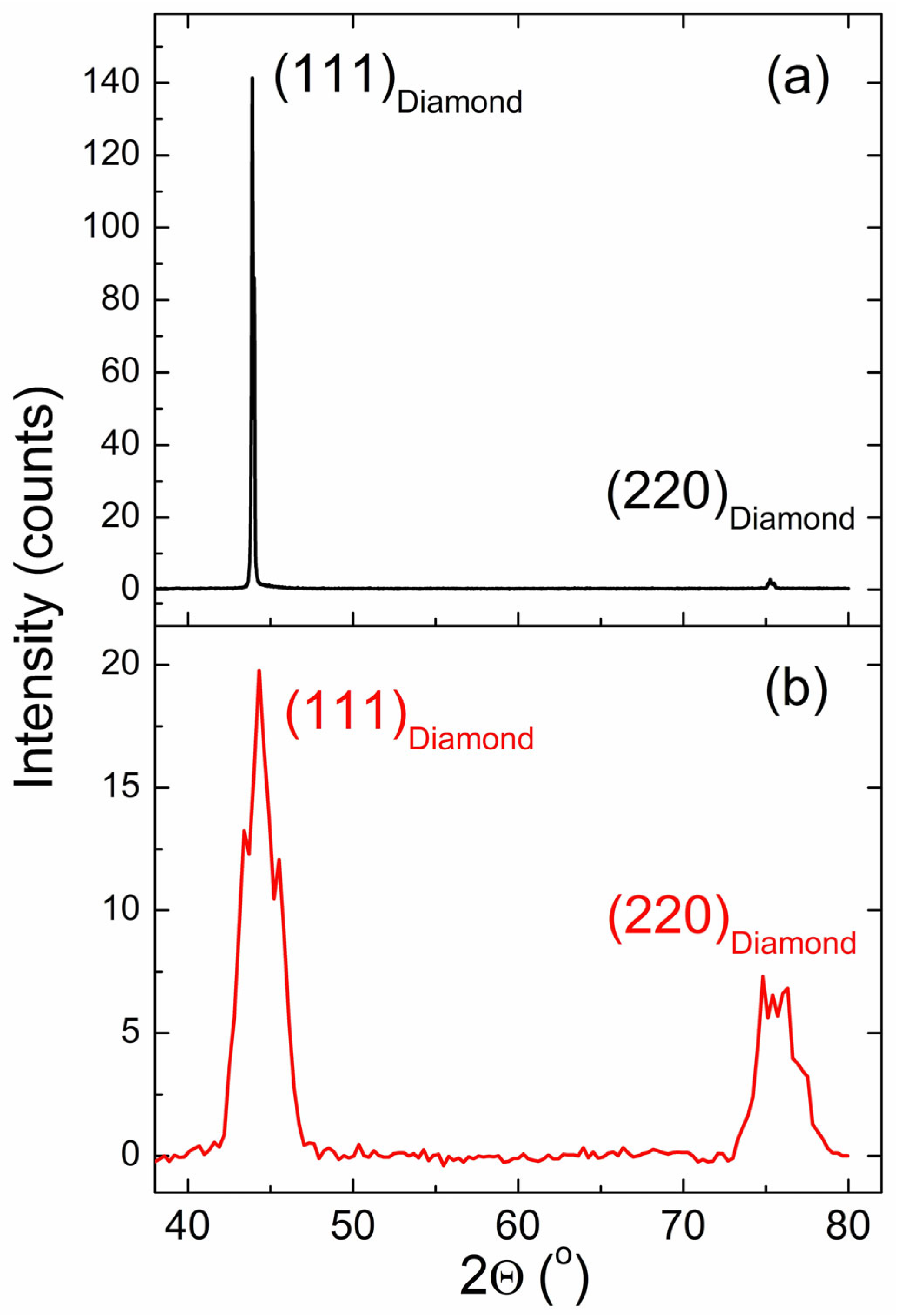
3.1. XRD Data
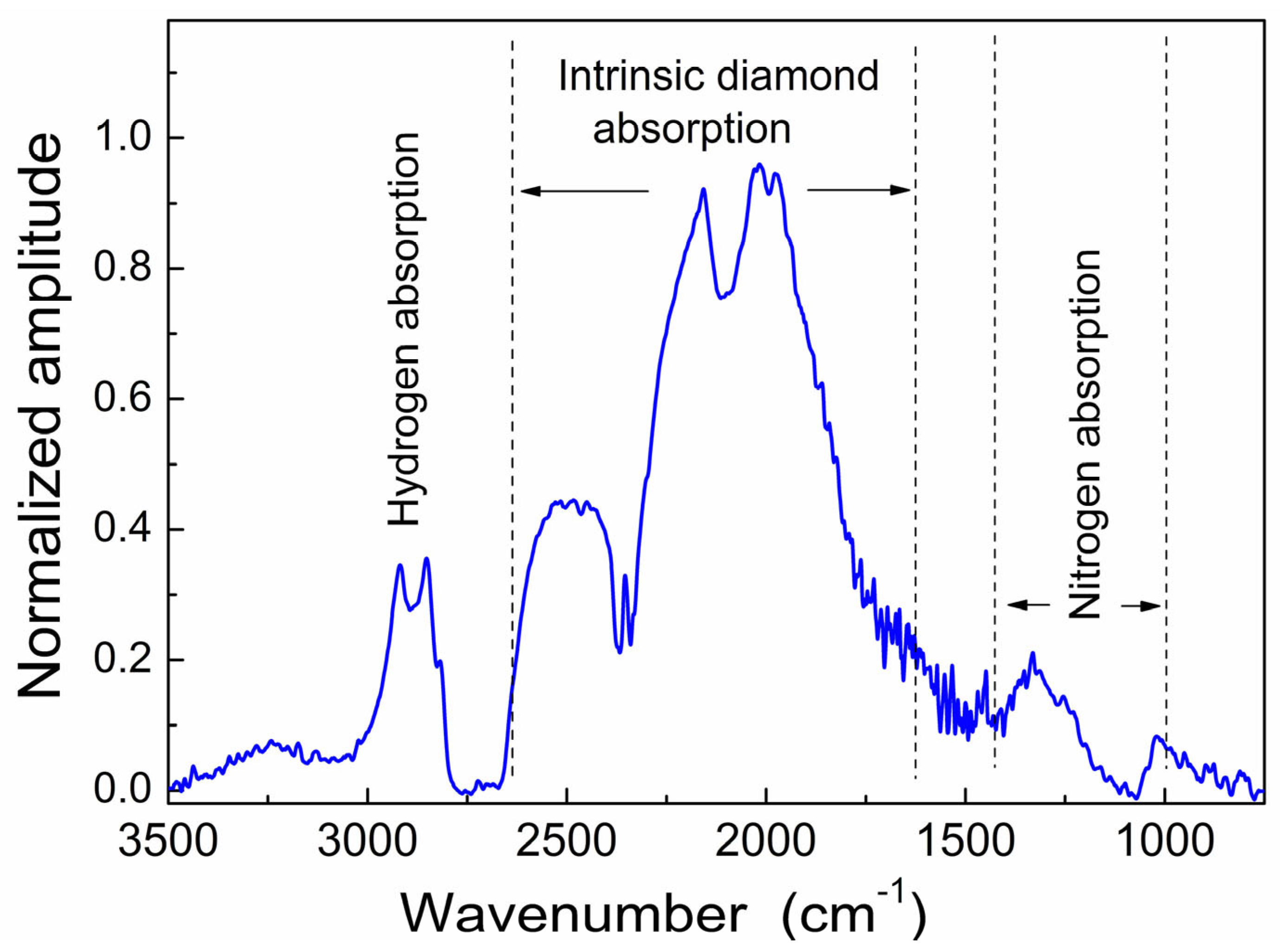
3.2. FTIR Spectra
3.3. EPR Data
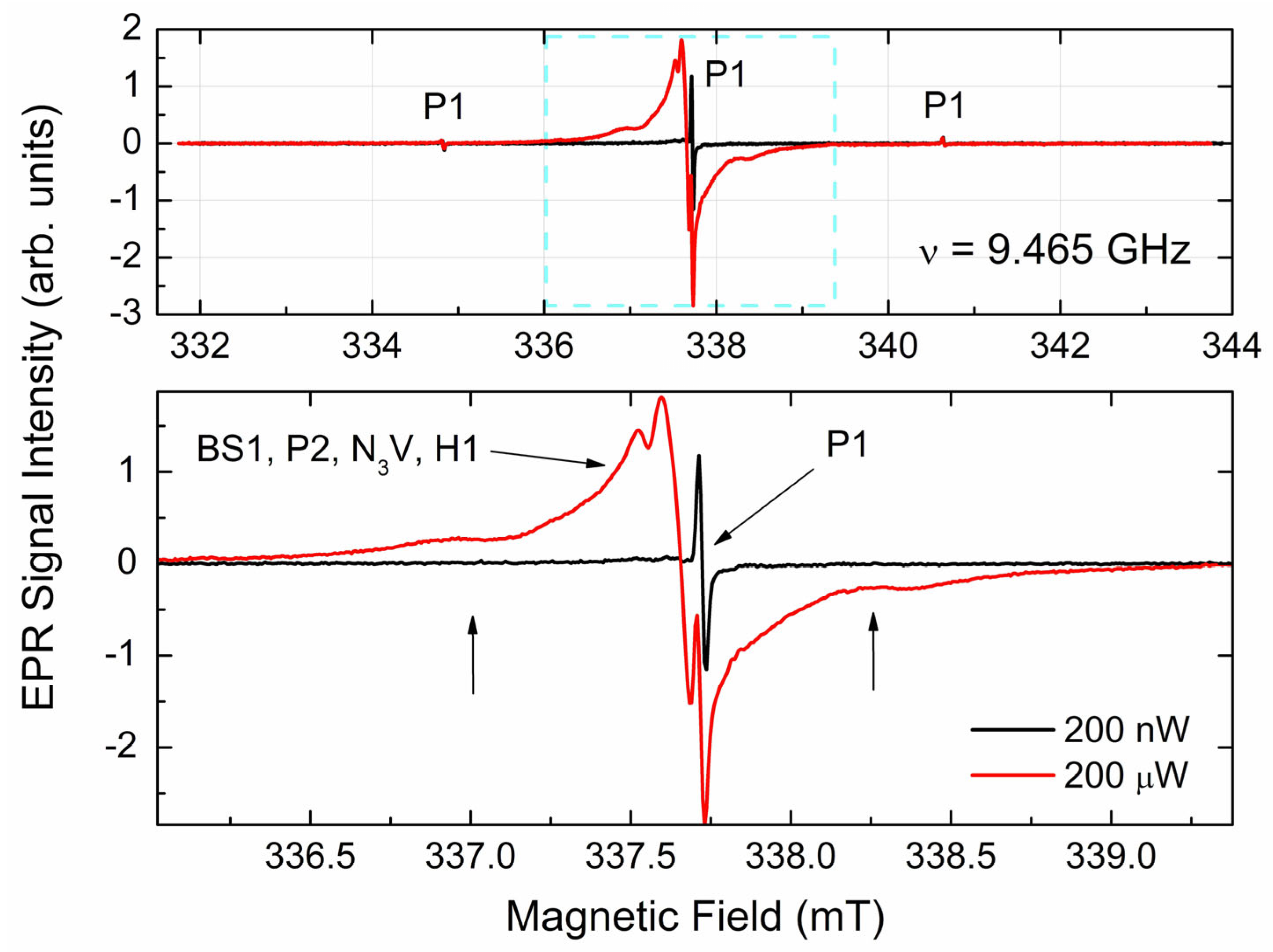
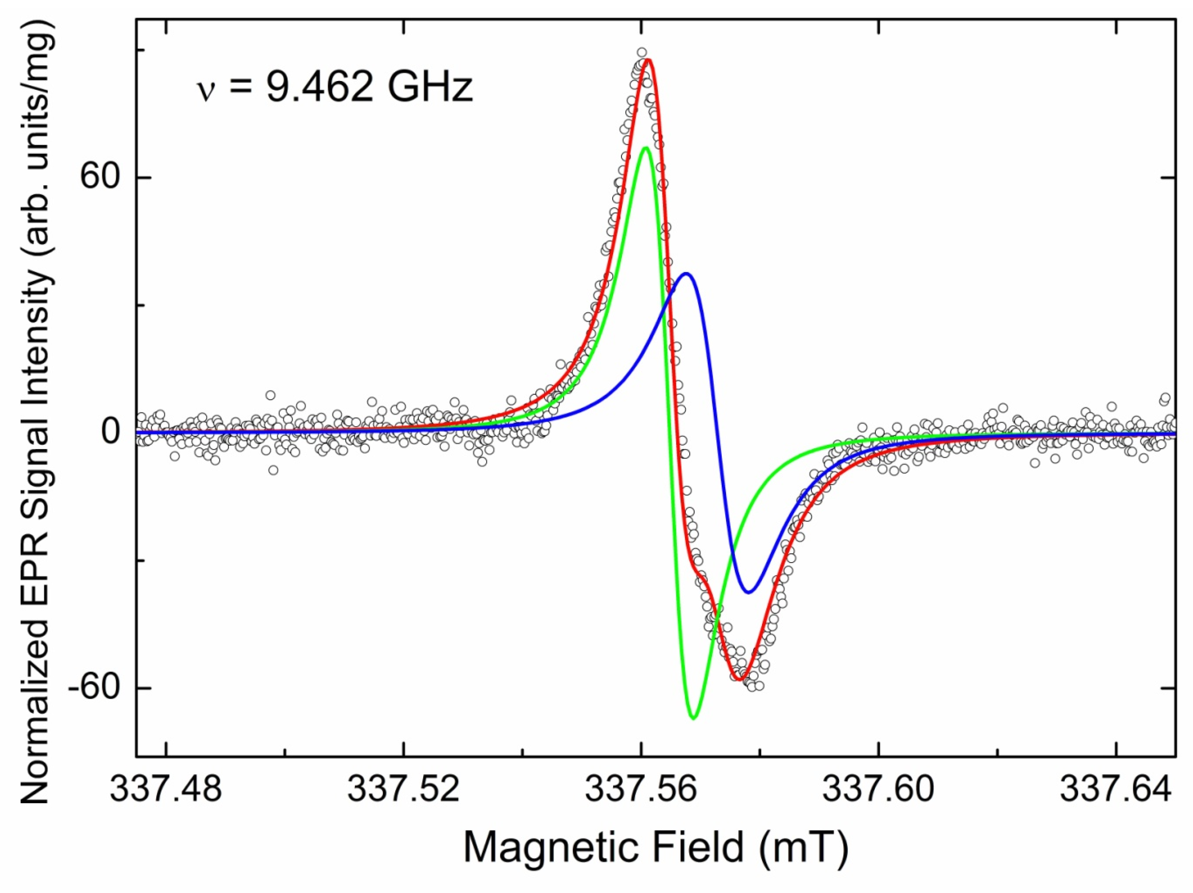
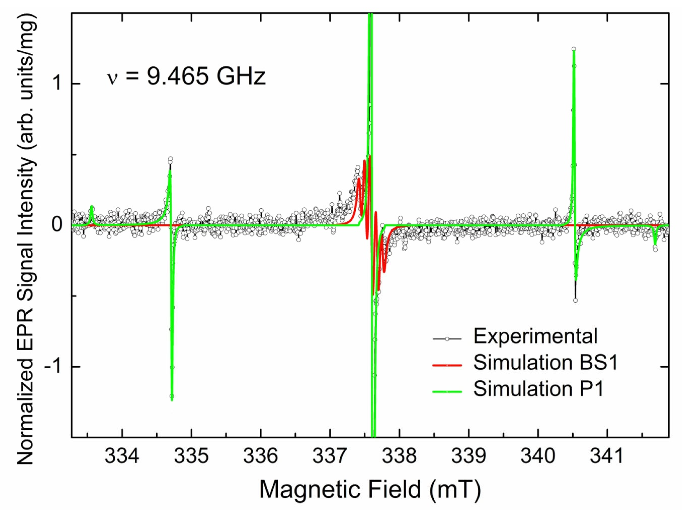
3.3.1. EPR Spectra of Primary Paramagnetic Centers
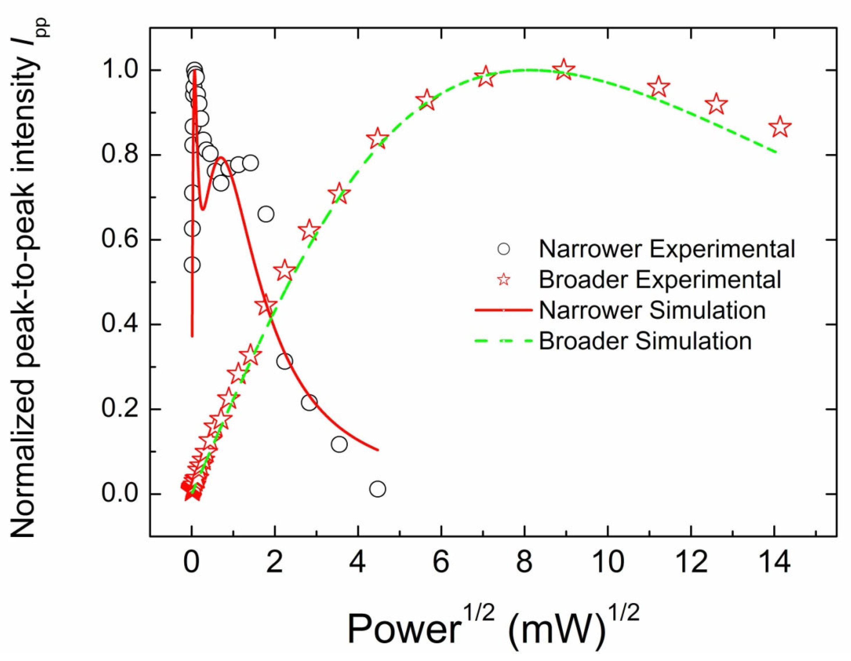
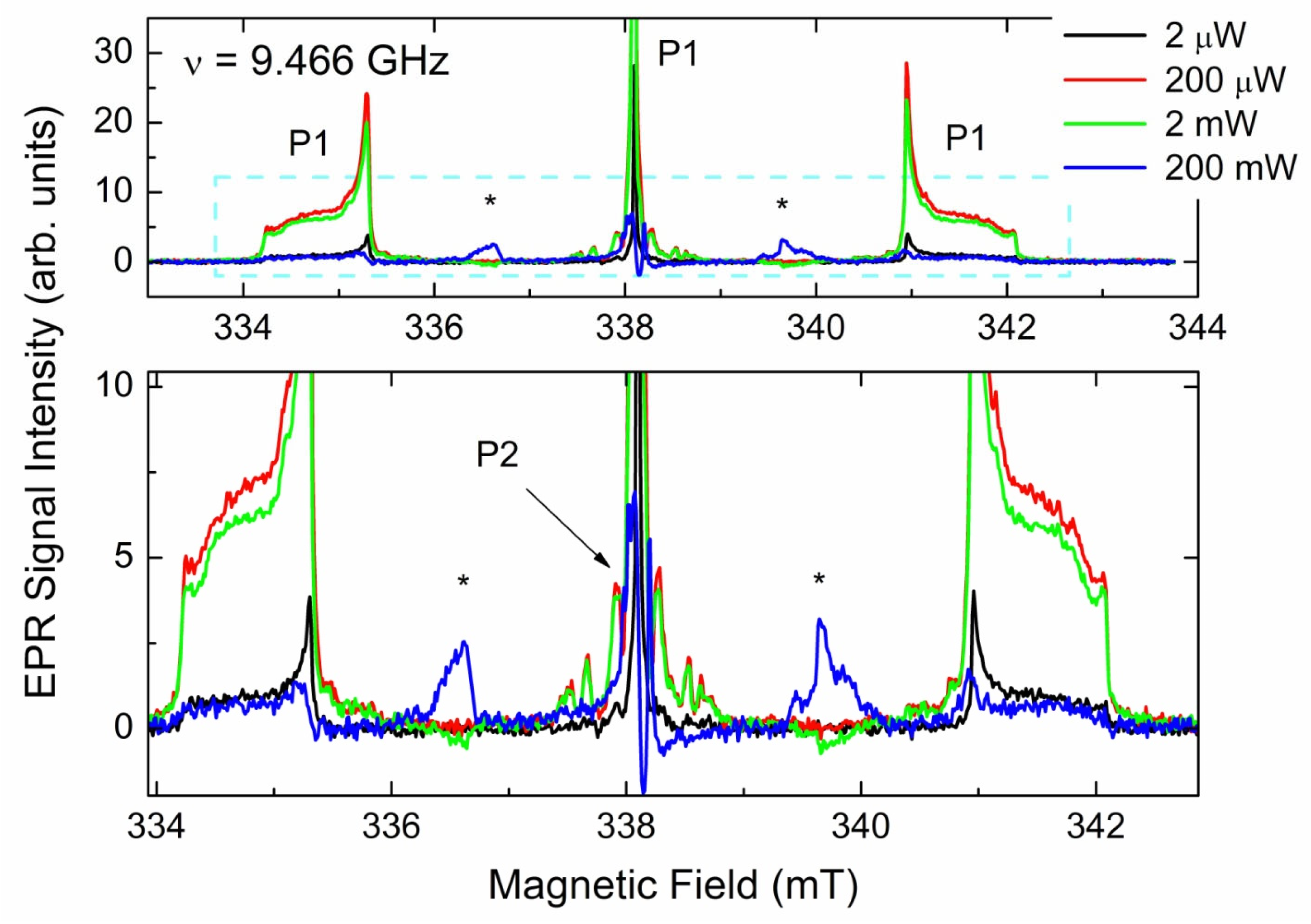
3.3.2. CW EPR Progressive Power Saturation of Primary Centers
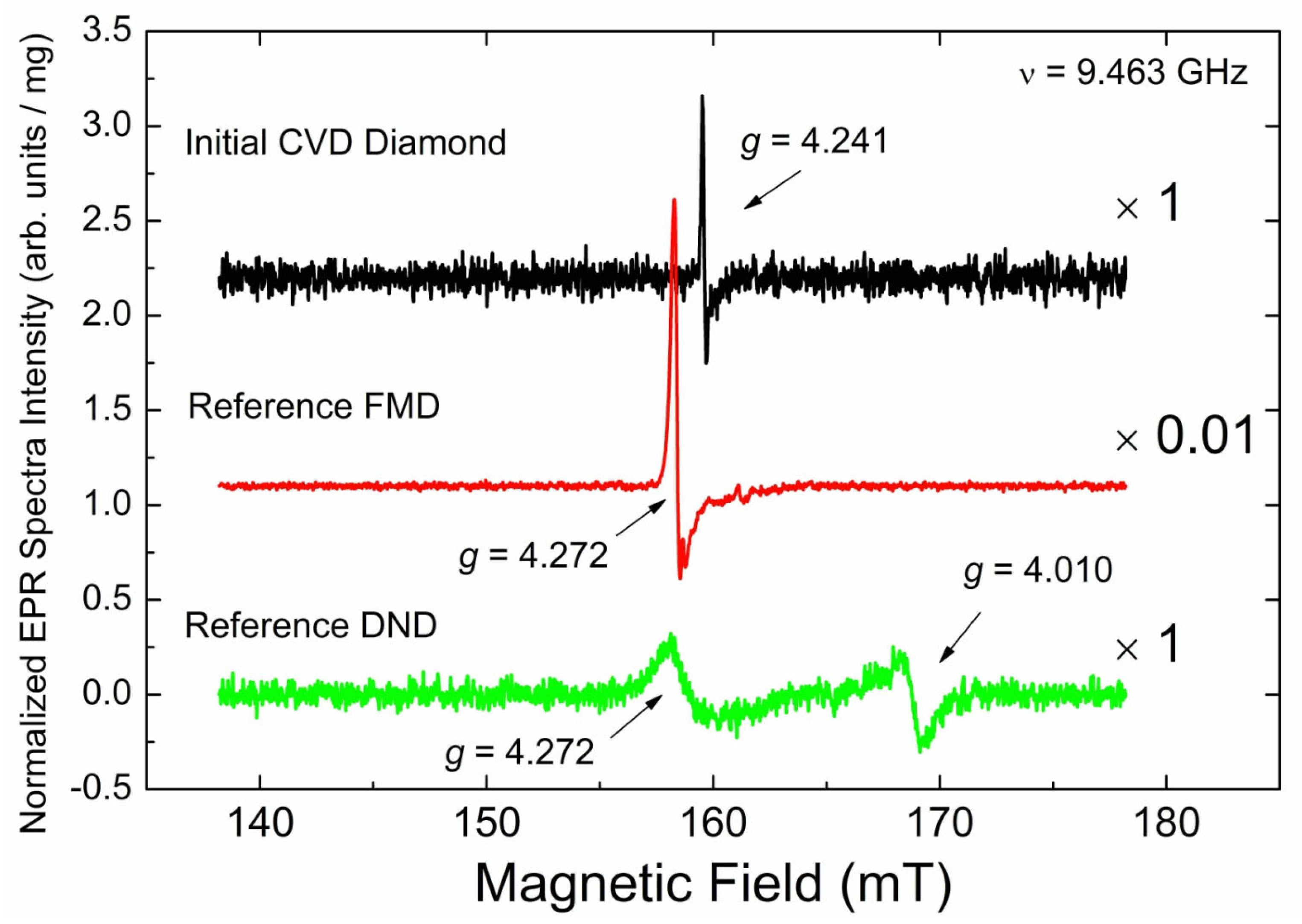
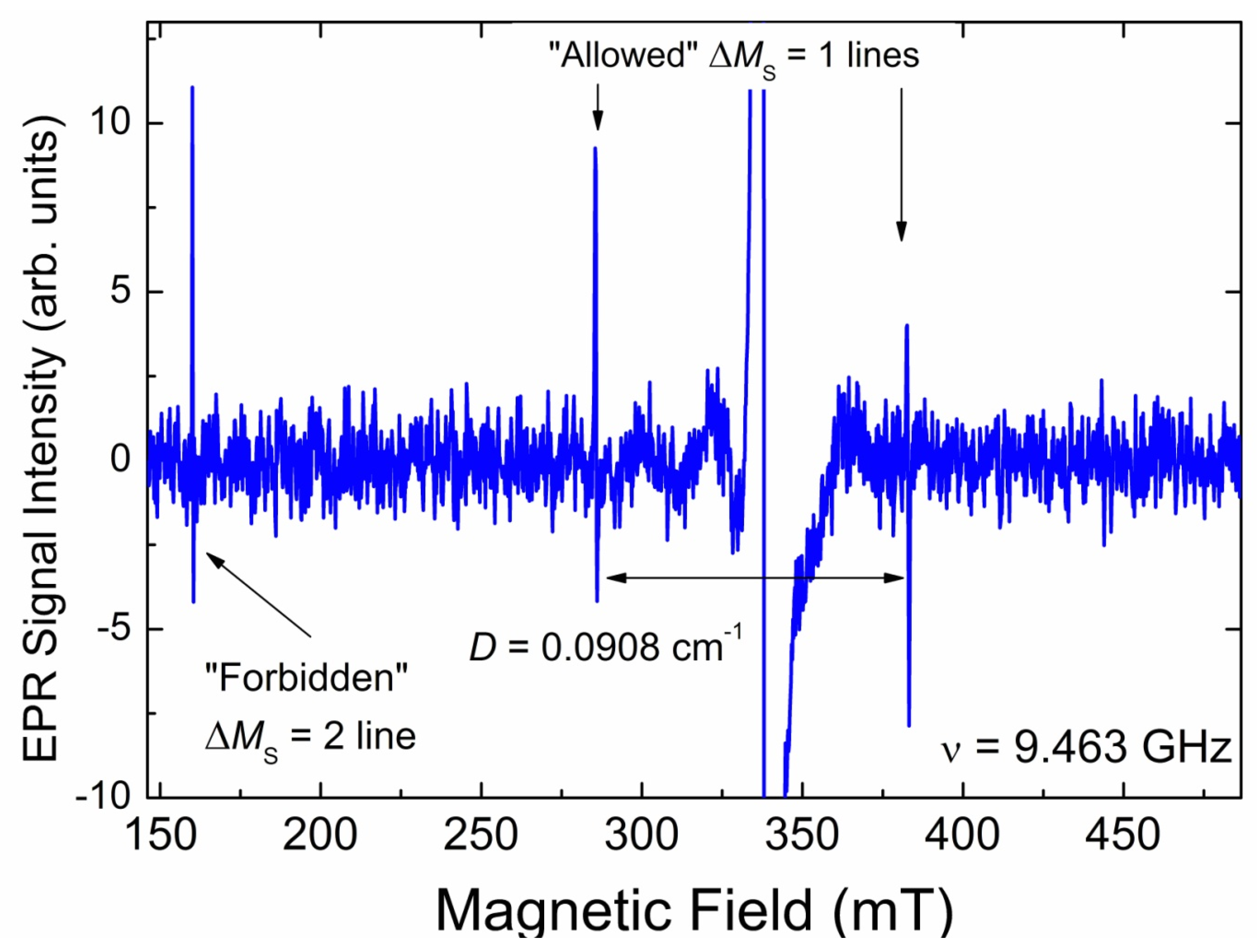
3.3.3. EPR Spectra of Triplet (S = 1) Paramagnetic Centers
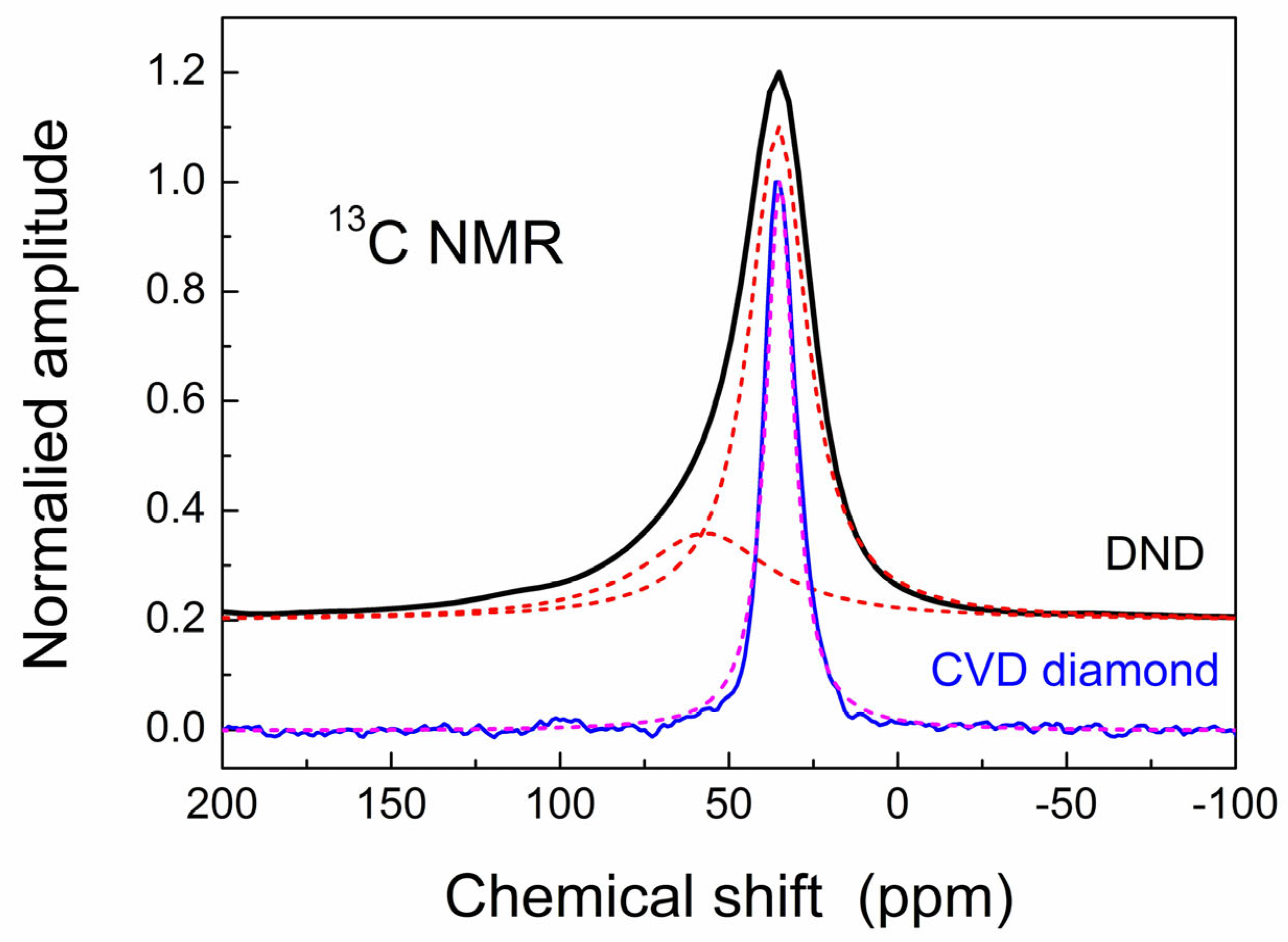
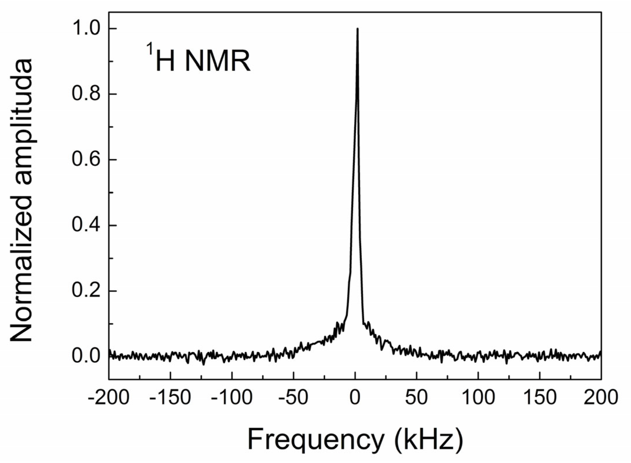
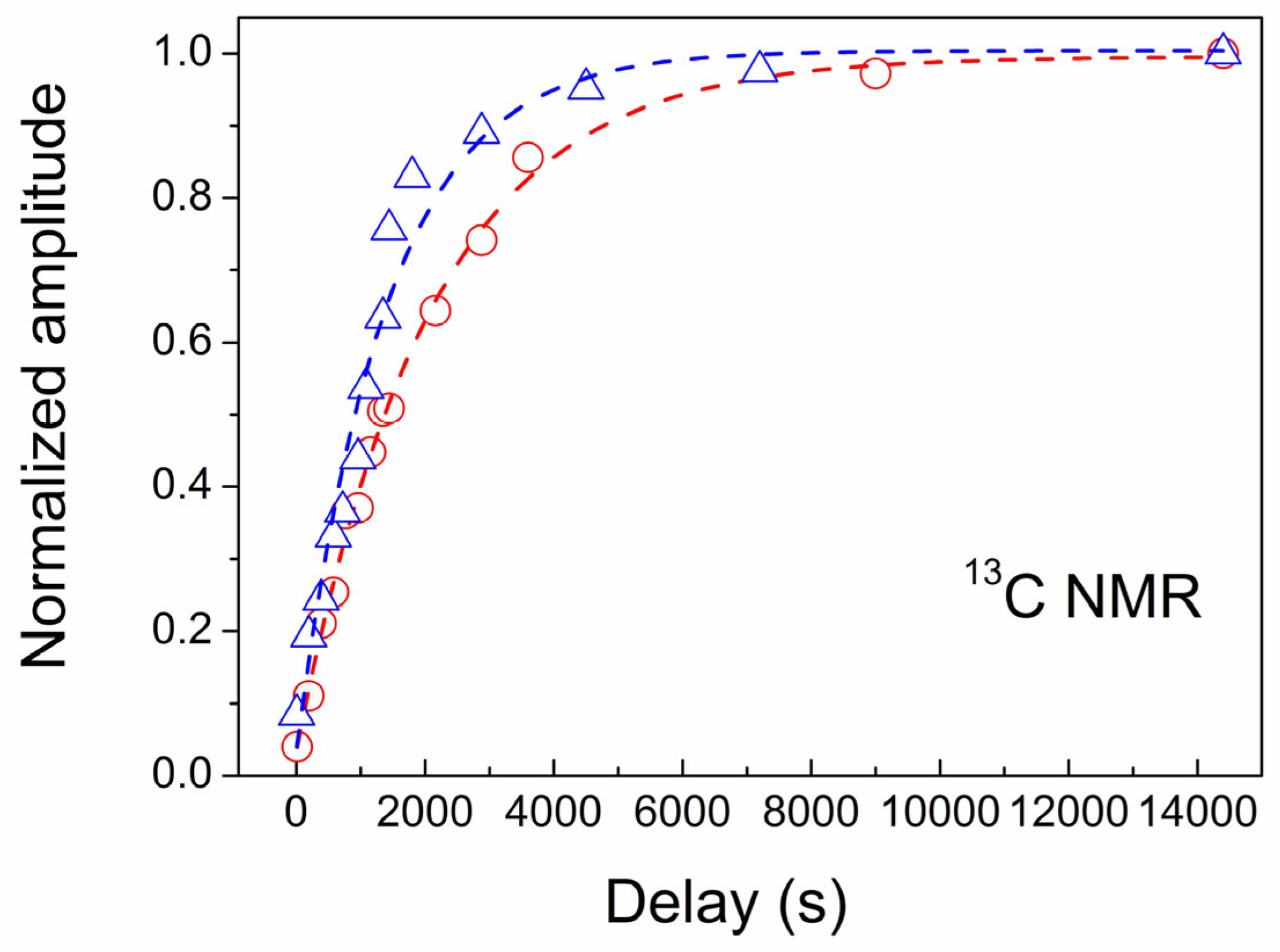
3.4. NMR Study of CVD Diamond
4. Discussion
5. Conclusions
Author Contributions
Funding
Institutional Review Board Statement
Informed Consent Statement
Data Availability Statement
Conflicts of Interest
References
- Goodwin, D.G.; Butler, J.E. Handbook of Industrial Diamonds and Diamond Films; Prelas, M.A., Popovici, G., Biglow, L.K., Eds.; Marcel Dekker, Inc.: New York, NY, USA, 1997; pp. 527–581. [Google Scholar]
- D’Haenens-Johansson, U.F.S.; Butler, J.E.; Katrusha, A.N. Synthesis of Diamonds and Their Identification. Rev. Mineral. Geochem. 2022, 88, 689–754. [Google Scholar] [CrossRef]
- Shames, A.I.; Panich, A.M.; Kempinski, W.; Baidakova, M.V.; Osipov, V.Y.; Enoki, T.; Vul’, A.Y. Magnetic resonance study of nanodiamonds. In Synthesis, Properties and Applications of Ultrananocrystalline Diamond; Gruen, D.M., Shenderova, O.A., Vul, A.Y., Eds.; NATO Science Series, Series II: Mathematics, Physics and Chemistry; Springer: Berlin/Heidelberg, Germany, 2005; Volume 192, pp. 271–282. Available online: https://books.google.co.il/books/about/Synthesis_Properties_and_Applications_of.html?id=gv5Nqsbr-ugC&redir_esc=y (accessed on 17 April 2024).
- Arnault, J.-C. (Ed.) Nanodiamonds: Advanced Material Analysis, Properties and Applications; Elsevier: Amsterdam, The Netherlands, 2017; 488p, Available online: https://www.elsevier.com/books/nanodiamonds/arnault/978-0-323-43029-6 (accessed on 17 April 2024).
- Wrachtrup, J.; Jelezko, F. Processing Quantum Information in Diamond. J. Phys. Condens. Matter 2006, 18, S807–S824. [Google Scholar] [CrossRef]
- Watanabe, I.; Sugato, K. EPR in diamond thin films sinthesized by microwave plasma chemical vapor deposition. Jpn. J. Appl. Phys. 1988, 27, 1808–1811. [Google Scholar] [CrossRef]
- Zhou, X.; Watkins, G.D.; Mcnamara-Rutledge, K.M.; Messmer, R.P.; Chawla, S. Hydrogen-related defects in polycrystalline CVD diamond. Phys. Rev. B 1996, 54, 7881–7890. [Google Scholar] [CrossRef]
- Rohrer, E.; Graeff, C.F.O.; Janssen, R.; Nebel, C.E.; Stutzmann, M.; Guttler, H.; Zachai, R. Nitrogen-related dopant and defect states in CVD diamond. Phys. Rev. B 1996, 54, 7874–7880. [Google Scholar] [CrossRef] [PubMed]
- Lukins, P.B.; Khachan, J. Power saturation and the effect of argon on the electron spin resonance of diamond deposited from a microwave plasma. Appl. Phys. Lett. 1994, 65, 3320–3322. [Google Scholar] [CrossRef]
- Talbot-Ponsonby, D. Paramagnetic Defects in CVD Diamonds. Ph.D. Thesis, University of Oxford, Oxford, UK, 1997. [Google Scholar]
- Hartland, C.B. A Study of Point Defects in CVD Diamond Using Electron Paramagnetic Resonance and Optical Spectroscopy. Ph.D. Thesis, University of Warwick, Coventry, UK, 2014. [Google Scholar]
- Ashfold, M.N.R.; Goss, J.P.; Green, B.L.; May, P.W.; Newton, M.E.; Peaker, C.V. Nitrogen in diamond. Chem. Rev. 2020, 120, 5745–5794. [Google Scholar] [CrossRef]
- May, P.W. Diamond thin films: A 21st-century material. Phil. Trans. R. Soc. Lond. A 2000, 358, 473–495. [Google Scholar] [CrossRef]
- Buijnstersa, J.G.; Shankarb, P.; van Enckevortc, W.J.P.; Schermerd, J.J.; Meulen, J.J.T. Adhesion analysis of polycrystalline diamond films on molybdenum by means of scratch, indentation and sand abrasion testing. Thin Solid Films 2005, 474, 186–196. [Google Scholar] [CrossRef]
- Kim, J.H.; Lee, S.K.; Kwon, O.M.; Lim, D.S. Ultra Thin CVD Diamond Film Deposition by Electrostatic Self-Assembly Seeding Process with Nano-Diamond Particles. J. Nanosci. Nanotechnol. 2009, 9, 4121. [Google Scholar] [CrossRef]
- Salenbien, R.; Sermeus, J.; Pobedinskas, P. Christ Glorieux1, Ken Haenen. Thin Nano- and Microcrystalline CVD Diamond Films for Micro-channel Cooling: Thermal and Elastic Properties. MRS Online Proc. Libr. 2010, 1282, 1502. [Google Scholar]
- Nemanich, R.J.; Carlisle, J.A.; Hirata, A.; Haenen, K. CVD diamond—Research, applications, and challenges. MRS Bulletin 2014, 39, 490. [Google Scholar] [CrossRef]
- Nistor, P.A.; May, P.W. Diamond thin films: Giving biomedical applications a new shine. J. R. Soc. Interface 2017, 14, 20170382. [Google Scholar] [CrossRef] [PubMed]
- Kratochvilova, I. Polycrystalline Diamond Thin Films for Advanced Applications. In Advances in Carbon Nanostructures; Silva, A.M.T., Carabineiro, S.A.C., Eds.; IntechOpen: London, UK, 2016; Chapter 8; pp. 161–173. Available online: https://www.intechopen.com/chapters/51835 (accessed on 17 April 2024).
- Polushin, N.I.; Laptev, A.I.; Spitsyn, B.V.; Alexenko, A.E.; Polyansky, A.M.; Maslov, A.L.; Martynova, T.V. Deposition of Boron-Doped Thin CVD Diamond Films from Methane-Triethyl Borate-Hydrogen Gas Mixture. Processes 2020, 8, 666. [Google Scholar] [CrossRef]
- Salvatori, S.; Pettinato, S.; Piccardi, A.; Sedov, V.; Voronin, A.; Ralchenko, V. Thin Diamond Film on Silicon Substrates for Pressure Sensor Fabrication. Materials 2020, 13, 3697. [Google Scholar] [CrossRef] [PubMed]
- Wei, S.; Xie, R.; Li, Y.; Meng, J.; Lin, R.; Weng, J.; Li, B. Deposition of diamond films by microwave plasma CVD on 4H-SiC Substrates. Mater. Res. Express 2023, 10, 126404. [Google Scholar] [CrossRef]
- Haddad, M.; Kurtulus, O.; Mertens, M.; Brühne, K.; Glüche, P.; Fecht, H. Optimization of residual stresses inside diamond thin films grown by hot filament chemical vapor deposition (HFCVD). Diamond Relat. Mater. 2023, 131, 109564. [Google Scholar] [CrossRef]
- Martyanov, A.; Tiazhelov, I.; Savin, S.; Voronov, V.; Konov, V.; Sedov, V. Synthesis of Polycrystalline Diamond Films in Microwave Plasma at Ultrahigh Concentrations of Methane. Coatings 2023, 13, 751. [Google Scholar] [CrossRef]
- Guo, X.; You, Y.; Bao, A.; Jia, P.; Xiong, J.; Li, J. Recent Progress of Nanodiamond Film in Controllable Fabrication and Field Emission Properties. Nanomaterials 2023, 13, 577. [Google Scholar] [CrossRef]
- Feng, M.; Jin, P.; Meng, X.; Xu, P.; Wu, J.; Wang, Z. One-step growth of a nearly 2 mm thick CVD single crystal diamond with an enlarged surface by optimizing the substrate holder structure. J. Crys. Growth 2023, 603, 127011. [Google Scholar] [CrossRef]
- Hu, X.; Li, M.; Wang, Y.; Peng, Y.; Tang, G.; Wang, X.; Li, B.; Yang, Y.; Xu, M.; Xu, X.; et al. Growth of 2-inch diamond films on 4H–SiC substrate by microwave plasma CVD for enhanced thermal performance. Vacuum 2023, 211, 111895. [Google Scholar] [CrossRef]
- Liang, Y.; Liu, K.; Liu, B.; Li, Y.; Fan, S.; Dai, B.; Zhang, Y.; Zhu, J. Vapor phase nucleation and sedimentation of dispersed nanodiamonds by MPCVD. Powder Technol. 2024, 436, 119507. [Google Scholar] [CrossRef]
- Bogdan, G.; De Corte, K.; Deferme, W.; Haenen, K.; Nesládek, M. Thick single crystal CVD diamond prepared from CH4-rich mixtures. Phys. Status Sol.a 2006, 203, 3063–3069. [Google Scholar] [CrossRef]
- Tallaire, A.; Achard, J.; Silva, F.; Brinza, O.; Gicquel, A. Growth of large size diamond single crystals by plasma assisted chemical vapour deposition: Recent achievements and remaining challenges. Comptes Rendus Phys. 2013, 14, 169–184. [Google Scholar] [CrossRef]
- Tallaire, A.; Mille, V.; Brinza, O.; Thi, T.N.T.; Brom, J.M.; Loguinov, Y.; Katrusha, A.; Koliadin, A.; Achard, J. Thick CVD diamond films grown on high-quality type IIa HPHT diamond substrates from New Diamond Technology. Diamond Relat. Mater. 2017, 77, 146–152. [Google Scholar] [CrossRef]
- Yamada, H.; Chayahara, A.; Mokuno, Y. Method to increase the thickness and quality of diamond layers using plasma chemical vapor deposition under (H, C, N, O) system. Diamond Relat. Mater. 2020, 101, 107652. [Google Scholar] [CrossRef]
- Osipov, V.Y.; Shames, A.I.; Enoki, T.; Takai, K.; Baidakova, M.V.; Vul, A.Y. Paramagnetic defects and exchange coupled spins in pristine ultrananocrystalline diamonds. Diam. Relat. Mater. 2007, 16, 2035–2038. [Google Scholar] [CrossRef]
- Nagy, V.Y.; Komozin, P.N.; Desrosiers, M.F. Choosing reference samples for EPR concentration measurements. Part 3. Systems of S = 3/2. Anal. Chim. Acta 1997, 339, 31–51. [Google Scholar] [CrossRef]
- Shames, A.I.; Osipov, V.Y.; Boudou, J.P.; Panich, A.M.; von Bardeleben, H.J.; Treussart, F.; Vul’, A.Y. Magnetic resonance tracking of fluorescent nanodiamond fabrication. J. Phys. D Appl. Phys. 2015, 48, 155302. [Google Scholar] [CrossRef]
- Stoll, S.; Schweiger, A. EasySpin, a comprehensive software package for spectral simulation and analysis in EPR. J. Magn. Reson. 2006, 178, 42–55. [Google Scholar] [CrossRef]
- Breeding, C.M.; Shigley, J.E. The ‘type’ classification system of diamonds and its importance in gemology. Gems Gemol. 2009, 45, 96–111. [Google Scholar] [CrossRef]
- Speich, L.; Kohn, S.C. QUIDDIT—Quantification of infrared active Defects in Diamond and Inferred Temperatures. Comput. Geosci. 2020, 144, 104558. [Google Scholar] [CrossRef]
- Loubser, J.H.N.; van Wyk, J.A. Electron spin resonance in the study of diamond. Rep. Prog. Phys. 1978, 41, 1201–1248. [Google Scholar] [CrossRef]
- Ammerlaan, C.A.J. Impurities and Defects in Group IV Elements and III-V Compounds; Springer: Berlin/Heidelberg, Germany, 1998; Volume 22, ISBN 978-3-540-48331-1. [Google Scholar]
- Portis, A.M. Rapid Passage Effects in Electron Spin Resonance. Phys. Rev. 1955, 100, 1219–1221. [Google Scholar] [CrossRef]
- Rovere, M.; Porro, S.; Musso, S.; Shames, A.I.; Williams, O.; Bruno, P.; Tagliaferro, A.; Gruen, D.M. Study of Detonation Nanodiamonds by Electron Paramagnetic Resonance. Diamond Relat. Mater. 2006, 15, 1913–1916. [Google Scholar] [CrossRef]
- Casabianca, L.B.; Shames, A.I.; Panich, A.M.; Shenderova, O.; Frydman, L. Factors Affecting DNP NMR in Polycrystalline Diamond Samples. J. Phys. Chem. C 2011, 115, 19041–19048. [Google Scholar] [CrossRef]
- Panich, A.M. Nuclear magnetic resonance studies of nanodiamonds. Crit. Rev. Solid State Mater. Sci. 2012, 37, 276–303. [Google Scholar] [CrossRef]
- Shames, A.I.; Mogilyansky, D.; Panich, A.M.; Sergeev, N.A.; Olszewski, M.; Boudou, J.P.; Osipov, V.Y. XRD, NMR, and EPR study of polycrystalline micro-and nano-diamonds prepared by a shock wave compression method. Phys. Status Solidi a 2015, 212, 2400–2409. [Google Scholar] [CrossRef]
- Panich, A.M.; Shames, A.I.; Mogilyansky, D.; Goren, S.D.; Dolmatov, V.Y. Detonation nanodiamonds fabricated from tetryl: Synthesis, NMR, EPR and XRD study. Diamond Relat. Mater. 2020, 108, 107918. [Google Scholar] [CrossRef]
- Panich, A.M. Nuclear magnetic resonance studies of nanodiamond surface modification. Diam. Relat. Mater. 2017, 79, 21–31. [Google Scholar] [CrossRef]
- Abragam, A. The Principles of Nuclear Magnetism; Clarendon Press: Oxford, UK, 1961. [Google Scholar]
- Goldman, M. Spin Temperature and Nuclear Magnetic Resonance in Solids; Clarendon Press: Oxford, UK, 1970. [Google Scholar]
- Shames, A.I.; Panich, A.M.; Kempiński, W.; Alexenskii, A.E.; Baidakova, M.V.; Dideikin, A.T.; Osipov, V.Y.; Siklitski, V.I.; Osawa, E.; Ozawa, M.; et al. Defects and impurities in nanodiamonds: EPR, NMR and TEM study. J. Phys. Chem. Solids 2002, 63, 1993–2001. [Google Scholar] [CrossRef]
- Shames, A.I.; Panich, A.M.; Porro, S.; Rovere, M.; Musso, S.; Tagliaferro, A.; Baidakova, M.V.; Osipov, V.Y.; Vul’, A.Y.; Enoki, T.; et al. Defects localization and nature in bulk and thin film utrananocrystalline diamond. Diam. Relat. Mater. 2007, 16, 1806–1812. [Google Scholar] [CrossRef]
- Panich, A.M. Universal Dependence of Nuclear Spin Relaxation on the Concentration of Paramagnetic Centers in Nano- and Microdiamonds. Materials 2022, 15, 5774. [Google Scholar] [CrossRef] [PubMed]
- Shames, A.I.; Panich, A.M.; Friedlander, L.; Dolmatov, V.Y. Magnetic resonance study of novel detonation nanodiamonds originated from non-conventional explosives. Diam. Relat. Mater. 2023, 136, 110059. [Google Scholar] [CrossRef]
- Mollart, T.P.; Lewis, K.L. The Infrared Optical Properties of CVD Diamond at Elevated Temperatures. Phys. Status Sol. a 2001, 186, 309–318. [Google Scholar] [CrossRef]
- McNamara, K.M.; Gleason, K.K. Radial Distribution of Hydrogen in Chemical Vapor Deposited Diamond. Chem. Mater. 1994, 6, 39–43. [Google Scholar] [CrossRef]
- Osipov, V.Y.; Shames, A.I.; Efimov, N.N.; Shakhov, F.M.; Kidalov, S.V.; Minin, V.V.; Vul’, A.Y. Evolution of triplet paramagnetic centers in diamonds obtained by sintering of detonation nanodiamonds at high pressure and temperature. Phys. Solid State 2018, 60, 723–729. [Google Scholar] [CrossRef]
- Nir-Arad, O.; Shlomi, D.H.; Manukovsky, N.; Laster, E.; Kaminker, I. Nitrogen Substitutions Aggregation and Clustering in Diamonds as Revealed by High-Field Electron Paramagnetic Resonance. J. Am. Chem. Soc. 2023, 146, 5100–5107. [Google Scholar] [CrossRef] [PubMed]
- van Wyk, J.A.; Reynhardt, E.C.; High, G.L.; Kiflawi, I. The dependences of ESR line widths and spin-spin relaxation times of single nitrogen defects on the concentration of nitrogen defects in diamond. J. Phys. D Appl. Phys. 1997, 30, 1790–1793. [Google Scholar]
- Nadolinny, V.A.; Shatsky, V.S.; Yuryeva, O.P.; Rakhmanova, M.I.; Komarovskikh, A.Y.; Kalinin, A.; Palyanov, Y.N. Formation features of N3V centers in diamonds from the Kholomolokh placer in the Northeast Siberian Craton. Phys. Chem. Miner. 2020, 47, 4. [Google Scholar] [CrossRef]
- van Wyk, J.A.; Loubser, J.H.N. Henderson; Diamond Conference: Bristol, UK, 1980; p. 90. [Google Scholar]
- Bloembergen, N. The interaction of nuclear spins in a crystalline lattice. Physica 1949, 15, 386–426. [Google Scholar] [CrossRef]
- Reynhardt, E.C.; High, G.L. Nuclear magnetic resonance studies of diamond. Prog. Nucl. Magn. Reson. Spectrosc. 2001, 38, 37–81. [Google Scholar] [CrossRef]
- Hoch, M.J.R.; Reynhardt, E.C. Nuclear spin-lattice relaxation of dilute spins in semiconducting diamond. Phys. Rev. B 1988, 37, 9222–9226. [Google Scholar] [CrossRef] [PubMed]


| Stage | Time, h | Pressure, torr | T, °C | Power, W | H2, sccm | CH4, sccm | O2, sccm |
|---|---|---|---|---|---|---|---|
| Nucleation | 60 | 115 | 836 | 4974 | 500 | 18 | 0.5 |
| Growth | 56.55 | 115 | 836 | 4974 | 478 | 20 | 2.0 |
| Sample | NS, ppm | T1, s |
|---|---|---|
| CVD-1 | 3 | 2070 ± 79 |
| CVD-2 | 5 | 1340 ± 126 |
Disclaimer/Publisher’s Note: The statements, opinions and data contained in all publications are solely those of the individual author(s) and contributor(s) and not of MDPI and/or the editor(s). MDPI and/or the editor(s) disclaim responsibility for any injury to people or property resulting from any ideas, methods, instructions or products referred to in the content. |
© 2024 by the authors. Licensee MDPI, Basel, Switzerland. This article is an open access article distributed under the terms and conditions of the Creative Commons Attribution (CC BY) license (https://creativecommons.org/licenses/by/4.0/).
Share and Cite
Shames, A.; Panich, A.; Friedlander, L.; Cohen, H.; Butler, J.; Moreh, R. Magnetic Resonance Study of Bulky CVD Diamond Disc. Materials 2024, 17, 1871. https://doi.org/10.3390/ma17081871
Shames A, Panich A, Friedlander L, Cohen H, Butler J, Moreh R. Magnetic Resonance Study of Bulky CVD Diamond Disc. Materials. 2024; 17(8):1871. https://doi.org/10.3390/ma17081871
Chicago/Turabian StyleShames, Alexander, Alexander Panich, Lonia Friedlander, Haim Cohen, James Butler, and Raymond Moreh. 2024. "Magnetic Resonance Study of Bulky CVD Diamond Disc" Materials 17, no. 8: 1871. https://doi.org/10.3390/ma17081871
APA StyleShames, A., Panich, A., Friedlander, L., Cohen, H., Butler, J., & Moreh, R. (2024). Magnetic Resonance Study of Bulky CVD Diamond Disc. Materials, 17(8), 1871. https://doi.org/10.3390/ma17081871