Article

Synthesis of Orthorhombic Tin Dioxide Nanowires in Track Templates

1
Department of Technical Physics, L.N. Gumilyov Eurasian National University, Satpayev Str. 2, Astana 010008, Kazakhstan
2
Faculty of Energy, Automation and Telecommunications, Abylkas Saginov Karaganda Technical University, Karaganda 100027, Kazakhstan
3
Department of Space Technique and Technology, L.N. Gumilyov Eurasian National University, Satpayev Str. 2, Astana 010008, Kazakhstan
4
Institute of Solid State Physics, University of Latvia, Kengaraga 8, LV-1063 Riga, Latvia
*
Authors to whom correspondence should be addressed.
Materials 2024, 17(6), 1226; https://doi.org/10.3390/ma17061226
Submission received: 3 February 2024 / Revised: 21 February 2024 / Accepted: 28 February 2024 / Published: 7 March 2024
(This article belongs to the Section Advanced Nanomaterials and Nanotechnology)

Abstract

:
Electrochemical deposition into a prepared SiO2/Si-p ion track template was used to make orthorhombic SnO2 vertical nanowires (NWs) for this study. As a result, a SnO2-NWs/SiO2/Si nanoheterostructure with an orthorhombic crystal structure of SnO2 nanowires was obtained. Photoluminescence excited by light with a wavelength of 240 nm has a low intensity, arising mainly due to defects such as oxygen vacancies and interstitial tin or tin with damaged bonds. The current–voltage characteristic measurement showed that the SnO2-NWs/SiO2/Si nanoheterostructure made this way has many p-n junctions.

1. Introduction

Contemporary materials science is currently focused on developing new materials and methods for oxide photonics, sensors, and optoelectronics [1]. This trend is aimed at creating smaller device sizes, with a particular focus on one-dimensional nanowire-based optoelectronic devices such as emitters [2,3], detectors [4,5], and transistors [6,7]. These devices are currently being actively developed.
SnO2 is an oxide semiconductor that is widely recognized for its unique electrical and optical properties. At 300 K, it has a band gap (Eg) of 3.6 eV and exhibits n-type conductivity. Due to its exceptional characteristics, including high electrical conductivity, low electrical resistance, and excellent optical transparency in the visible spectrum, SnO2 has been extensively studied for various applications. It is commonly used in the manufacturing of transparent conductors [8], transistors [6,7,9], optoelectronic devices [10,11], gas sensors [12], and more.
There are various types of tin oxide in nanoform. By constructing low-dimensional nanostructures on semiconductor oxides, it is possible to create and design new material systems with unique properties. Nanowires (NWs), for example, can support nanoparticles, other nanowires, and nanosheets, providing access to designs that were previously unattainable with conventional thin-film technology. Molecular beam epitaxy (MBE) and chemical vapor deposition (CVD) are regulated processes used to produce high-quality nanomaterials. The interaction between the physical characteristics of oxides and the 1D shape of NWs makes oxide wide-gap semiconductors (WBGs) an excellent technological foundation.
Producing oxide nanomaterials with consistent morphologies and physical properties is a major challenge due to their lack of repeatability. Unlike group III-V semiconductors, manufacturing such structures is often complex and poorly understood. However, self-assembly mechanisms can provide the necessary repeatability and facilitate the “bottom-up” fabrication method [13].
One of the simplest techniques for creating nanowires is using nanoporous templates. The template synthesis method, which utilizes porous materials such as track membranes made of polyethylene terephthalate (PET), is a potential strategy for creating nanostructures. Electrochemical deposition can produce Fe/Co nanotubes on these PET membranes [14]. Other studies have produced Ni/Fe nanotubes and silver/gold nanoparticle-embedded nanotubes [15,16]. In a separate study, a simple process for electrochemical deposition in PET membranes was proposed to create nanotubes made of zinc. That study found that by annealing the resulting nanotubes, it is possible to control the production of an oxide phase in the nanostructure.
Due to their compatibility with existing silicon technology and their potential for application in the creation of track templates, thin nanoporous SiO2 layers incorporated into silicon wafers present intriguing advantages for nanotechnology. These templates, which are made up of nanoporous arrays that have been etched onto the location of latent tracks in SiO2, can be filled with a range of substances and composites.
The resultant structures could be used as low-temperature magnetic field sensors [17], biosensors [18,19], active electrical circuit elements [20], and more. These structures on Si wafers were produced using SHI track technology, which is only one illustration of the potential this novel strategy offers.
Due to the self-organization of WBG inside nanochannels, different structures can be obtained using this method. The template was created from a SiO2/Si structure using track technology, which includes irradiation with swift heavy ions and a chemical etching process [21,22]. Next, filling the nanopores with various materials is carried out. In our case, we are considering the possibility of tin dioxide precipitation.
An attractive aspect of template synthesis [23] is the ability to tailor a nanomaterial’s physical, chemical, and electronic properties through controlled manipulation of morphology, pore density, shape, and size. Our works demonstrate successful template synthesis of ZnO [23], CdTe [24], and ZnSe2O5 [25], resulting in stable phases of these compounds as well as phases that are typically only obtainable under special conditions.
This study aimed to form SnO2-NWs/SiO2/Si nanoheterostructures with arrays of p-n junctions and experimental/theoretical investigations of physical properties of obtained nanostructures. In order to corroborate our experimental results and better understand the electronic structure of the resulting SnO2 nanostructures, we simulated the electronic band structure along with the total density of states using the CRYSTAL-17 program [26]. Calculation details are presented in the Materials and Methods section.

2. Materials and Methods

In the present work, the SiO2/Si (p-type) structure was formed by thermal oxidation of silicon substrate in a wet oxygen atmosphere at T = 900℃. According to ellipsometry, the thickness of the oxide layer was 700 nm. Irradiation of 10 × 10 mm2 SiO2/Si samples to create latent tracks in the SiO2 layer was carried out at a DC-60 cyclotron (Joint Institute for Nuclear Research (JINR) Dubna, Russia). The samples were bombarded at normal incidence with 200 MeV 132Xe ions to a fluence of 108 cm−2.
Etching in 4% aqueous HF solution was carried out to form nanoporous SiO2 layers irradiated with Xe ions. The etchant included m(Pd) = 0.025 g. The process of etching was performed at room temperature for a certain duration. The nanopore sizes were controlled depending on the etching time. After treatment in HF, the samples were washed in deionized water (18.2 MΩ). Electrochemical deposition (ECD) and chemical deposition (CD) were used to fill the nanochannels [27]. The template synthesis was carried out immediately after sensitization of surface and etching. The template synthesis (chemical and electrochemical deposition of materials) was a universal and simple method of receiving arranged arrays of nanostructures in matrix channels.
The electrolyte used to obtain SnO2-NWs/SiO2/Si, contained 6 g/L SnCl2–25 mL H2O–2 mL HCl. The composition solution was stirred using a magnetic stirrer while adding hydrochloric acid dropwise until the pH was between 2 and 4, stirring continuously until a clear solution formed. For the ECD process, a cell that was specifically prepared and a VersaStat 3 potentiostat were utilized. The ECD process was carried out at room temperature. A two-beam scanning microscope controlled the filling of nanopores, the Zeiss Crossbeam 540 (Jena, Germany).
X-ray diffraction analysis (XRD) provided detailed information on the structure and phase composition of the samples. Diffractograms were recorded using a Rigaku SmartLab X-ray diffractometer (Rigaku, Tokyo, Japan) with a high-energy resolution 2D HPAD detector HyPix3000 (Rigaku, Tikyo, Japan) in the 2θ range from 5 to 70° at 40 kV. When analyzing the diffraction patterns, we used TOPAS 4.2 software and the international ICDD database (PDF-2 Release 2020 RDB) to identify the phase composition and unit cell parameters of substances. This method enabled us to determine the structures of over 200,000 different compounds.
Photoluminescence spectra were measured at room temperature using a spectrofluorometer CM2203 (Solar, Minsk, Belarus) in the spectral range from 320 to 600 nm when excited by light with a wavelength of λ = 240 nm. Using two double monochromators ensured a minimum level of interference, guaranteeing high measurement accuracy.
A VersaStat 3 potentiostat/galvanostat (Ametek, Berwyn, PA, USA) was used to study the electrical properties of the resulting nanowire arrays. Current–voltage characteristics were measured from an array of filled nanochannels with an area of 0.7 cm2.
As noted above, we performed hybrid “large scale” DFT calculations of the structural and electronic properties of obtained SnO2 nanostructures in the framework of a periodic linear combination of atomic orbitals (LCAO) approximation. All calculations were made using the primitive crystal cell containing 24 atoms. The all-electron Gaussian-type basis sets (BS) for Sn and O atoms were taken from refs. [28,29], respectively. The total energy convergence threshold for the self-consistent field (SCF) procedure was chosen at 107 Hartree for structure relaxation calculations. The exchange and correlation effects were treated by using a B3LYP functional form (i.e., Becke’s three-parameter hybrid exchange functional [30] and Lee, Yang, Parr correlation functional [31]). It is worth noting that the hybrid B3LYP functional allows us to perform very accurate calculations of the band gap which are in good agreement with the corresponding experimental values. The integration of the reciprocal space was performed with a Pack–Monkhorst 4 × 4 × 4 grid. The effective atomic charges were determined using the Mulliken population analysis [32].

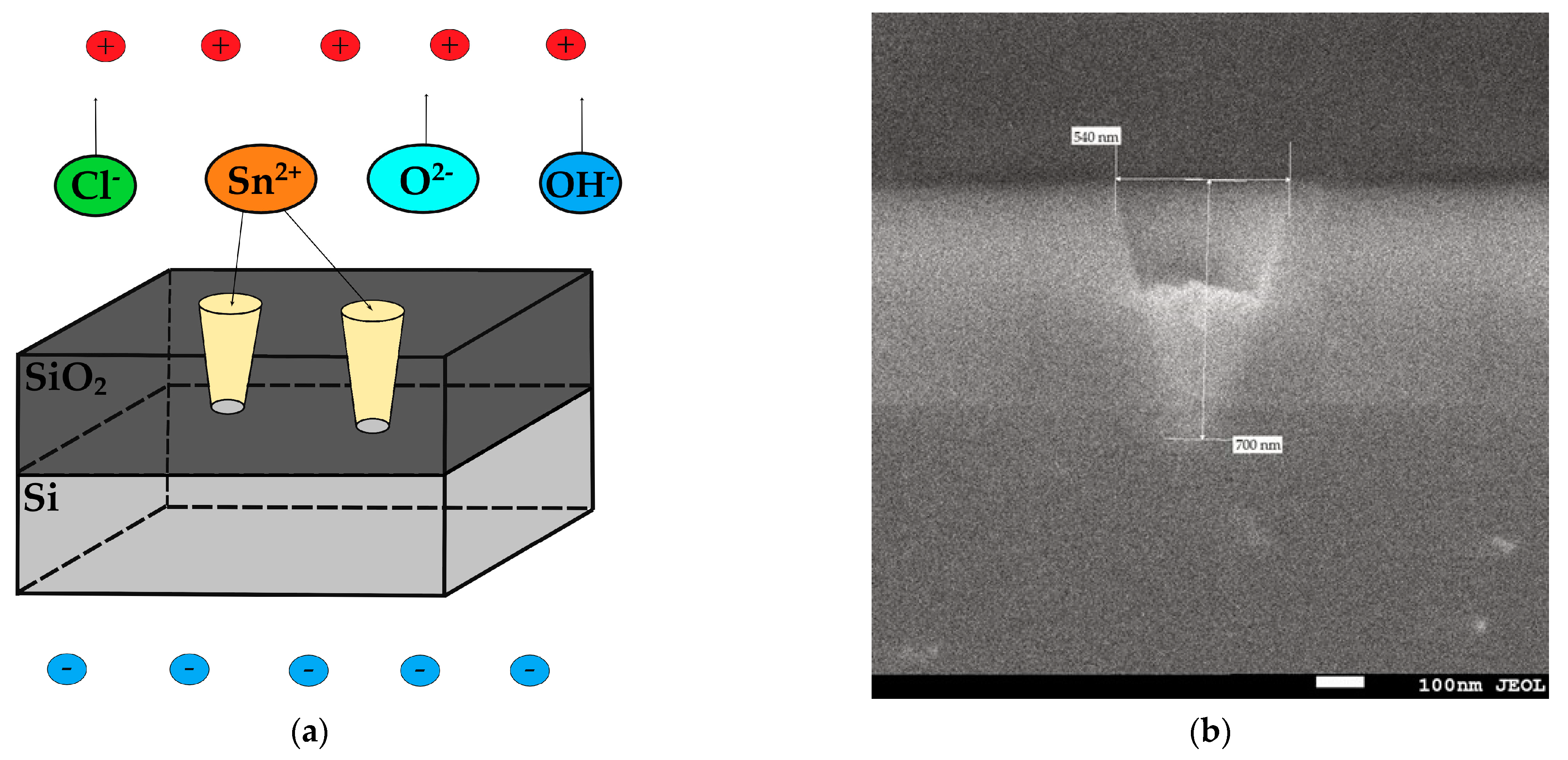
3. Results and Discussion

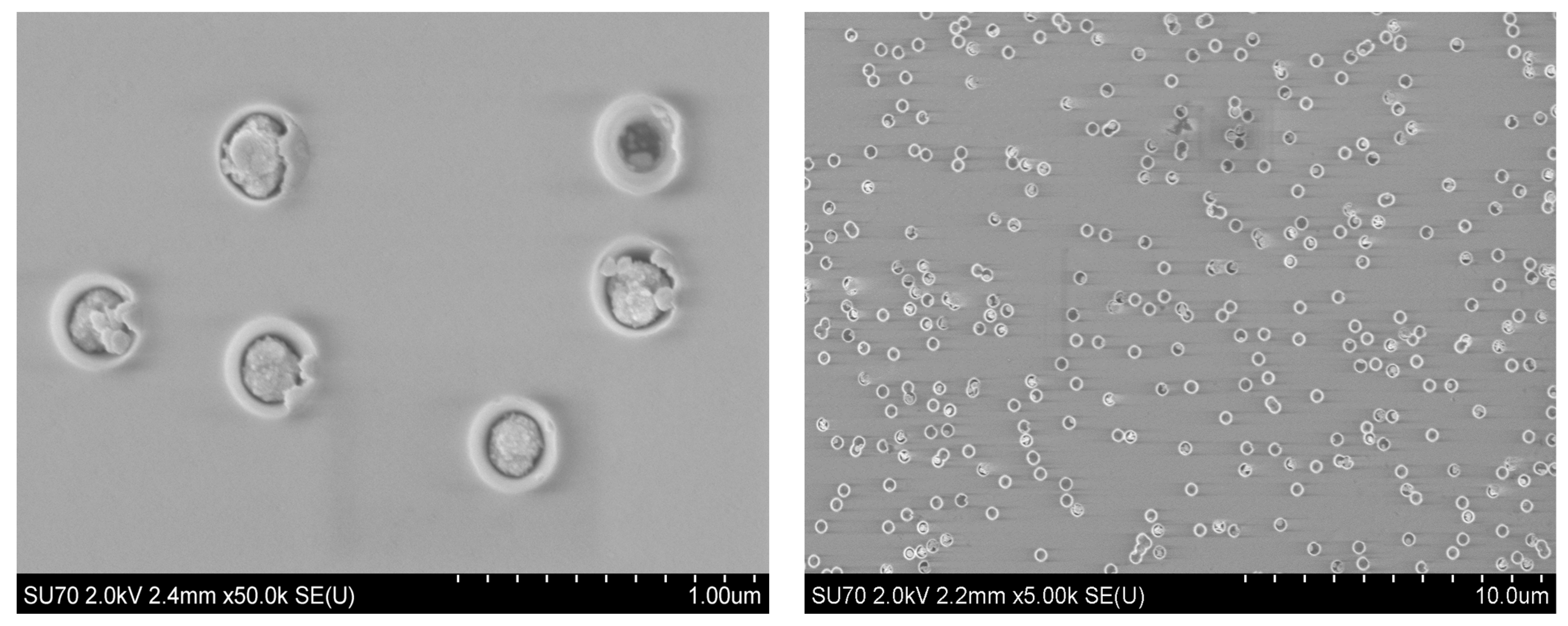
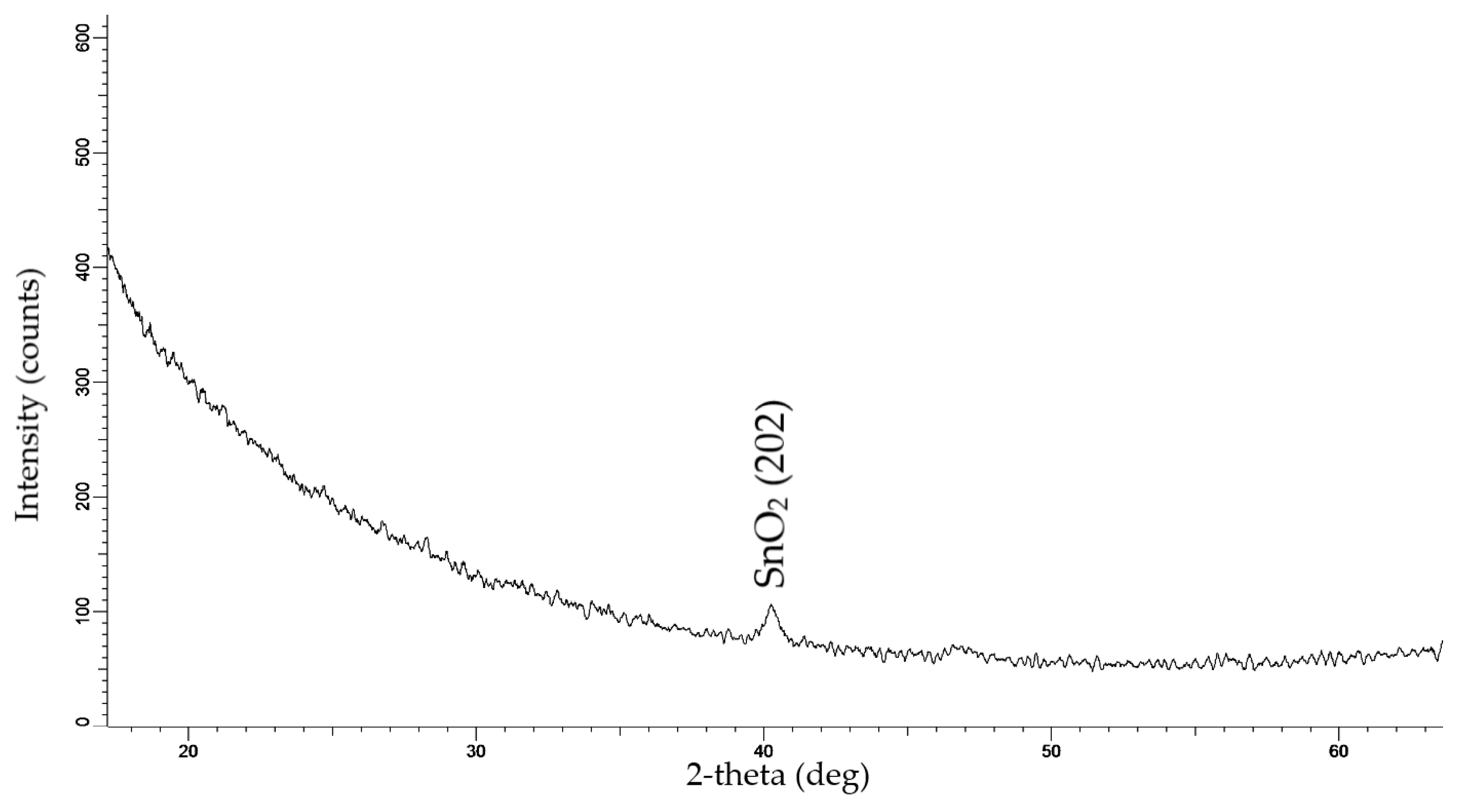
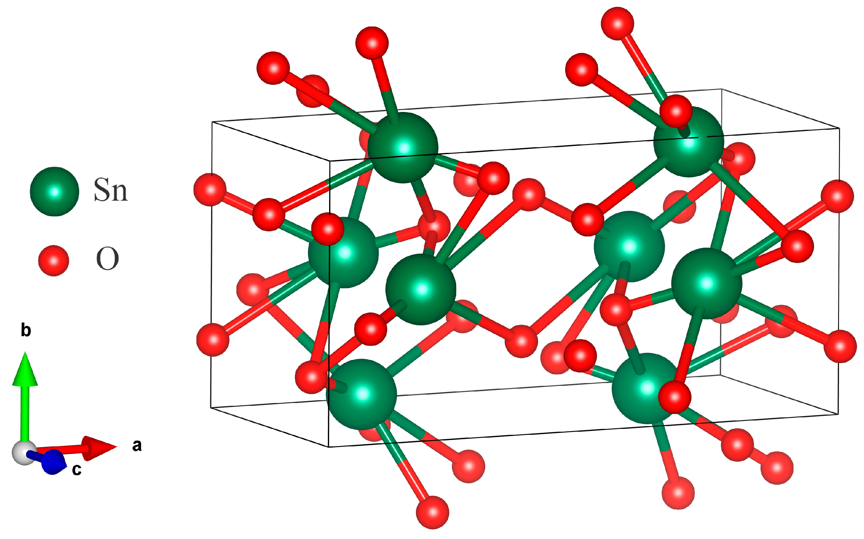
3.1. SEM and XRD Analysis of Deposited Samples

Figure 1 shows SEM images of the surface after deposition.
Figure 1 shows the SEM images of the surface after electrochemical deposition. SEM image analysis revealed nanopore diameters ranging from 519 nm to 562 nm. The amount of filled nanochannels was 87%.
According to XRD data (Figure 2), electrochemical deposition in a chloride solution into a SiO2/Si track template led to the creation of SnO2 nanowires with an orthorhombic structure and Pbca (61) space group symmetry. The results of the XRD analysis of the sample are summarized in Table 1.
We calculated the band structure along the highly symmetric k-points of the Brillion zone along with the density of states (Figure 3). The lattice parameters of relaxed crystal geometry were also calculated (see Table 1) The maximum of the valence band and the bottom of the conduction band were located at the Г-point with a band gap of 3.76 eV, which had good agreement with the previous studies using GGA-PBE [33] and the augmented plane wave (APW) methods [34]. It is worth noting, however, that various experimental estimates of the band gap vary from 1.7 to 4 eV [35,36,37]. Nagasawa et al. [38] studied the temperature dependence of the absorption edge for two polarizations of light; they showed a strong dependence of the optical adsorption edge on both factors. For both polarizations, the band gap decreases with increasing temperature. Figure 3 shows good agreement between theory and experiment. In particular, we find a valence band width of ~8 eV in good agreement with both experimental data (7.5 eV reported in ref. [39]) and previous first-principles calculations (7.9 eV and 8.8 eV reported in ref. [40] using PSP and USP, respectively). O-2p states mainly form the uppermost valence band, while the bottom of the conduction band is mostly the result of the contribution of Sn-4d orbitals with a hybridization of O-2p orbitals.
It is known that SnO2 crystallizes as a single crystal in the rutile, tetragonal structure (cassiterite) phase SnO2-(T). Rutile was typically used as the crystalline phase when this material was created as a nanostructure. However, as with many other materials, the crystal lattice changes under special conditions, such as high pressure, and the crystallographic phase becomes different. The study of [41] was one of the first to synthesize the orthorhombic phase SnO2-(O) of tin dioxide. The synthesis process was carried out using a split-sphere high-pressure vessel featuring an inner and outer layer. The container holds the sphere with samples, which is immersed in liquid. As the fluid pressure rises, the sphere is uniformly compressed. The samples in the center of the sphere are subjected to controlled pressure. The temperature was maintained by a small furnace tube. In this experiment, the SnO2-(O) polymorph with lattice parameters a = 4.714 Å, b = 5.727 Å, and c = 5.214 Å was synthesized at a pressure of 15.8 GPa and a temperature of 800 °C.
Unique studies of polymorphic transformations in SnO2 (cassiterite) were conducted in [42]. In situ, XRD analysis of the structure at increasing pressure and temperature showed the existence of four phase transitions up to 117 GPa. Cassiterite powder was mixed with 10 wt% Pt and located into a special cell. Platinum was used as a laser absorber and pressure standard. Starting from the rutile structure, the sequence of polymorphic transformations is as follows: rutile-type with space group P42/mnm transforms to CaCl2−type, Pnnm, which then transforms to pyrite-type, Pa3. The pyrite-type, Pa3, then transforms to ZrO2 orthorhombic phase I (O I), Pbca, and the last transformation is to cotunnite-type (Pnam) orthorhombic phase II (O II). The first three polymorph phases were found to be in general agreement with the results of previous studies. The orthorhombic phase O I and orthorhombic phase O II were observed in SnO2 for the first time. So, the (O I) Pbca phase formed at room temperature and 50–74 GPa pressure. The lattice parameters for this structure were determined and are as follows: a = 9.304 Å, b = 4.893 Å, and c = 4.731 Å. These values closely resemble those obtained in track template synthesis by ECD and our theoretical calculations (Table 1). Thus, the template synthesis (ECD) yielded orthorhombic SnO2 with a ZrO2-type crystal structure (orthorhombic phase I). We created a unit cell of SnO2 Pbca using our own data (Figure 4).
As can be seen, orthorhombic SnO2 is more difficult to fabricate as high pressure and temperature are required. But creating orthorhombic SnO2 in nanoforms, in the form of thin films, turns out to be a more affordable option. Several research groups have successfully created orthorhombic SnO2 thin films using different techniques at moderately low pressures and temperature [43,44,45,46,47,48,49].
Only a small fraction of the studies mention the preparation of the orthorhombic phase of tin dioxide nanowires, although many papers are devoted to the preparation of tin dioxide NWs (see [50,51,52,53] and references cited therein). SnO2 nanoribbons/nanowires were synthesized using elevated temperature synthesis techniques in inert Ar gas [54,55]. The authors suggest that orthorhombic SnO2 may be the result of product formation in an oxygen-deficient environment. The description of atypical structures in nanowires created using a template method or by adding catalytic in a vapor–liquid–solid method for different materials is presented in [56,57,58]. The authors of [59] conducted a study on the synthesis of pure single-crystal orthorhombic SnO2 as well as SnO2 nanowires that were decorated with cassiterite nanoclusters.
Based on our literature analysis, we found that using the template synthesis method provides us with the opportunity to successfully obtain tin dioxide with ZrO2 orthorhombic phase I (O I), Pbca nanowires, and nanoheterostructure (SnO2-NWs/SiO2/Si).

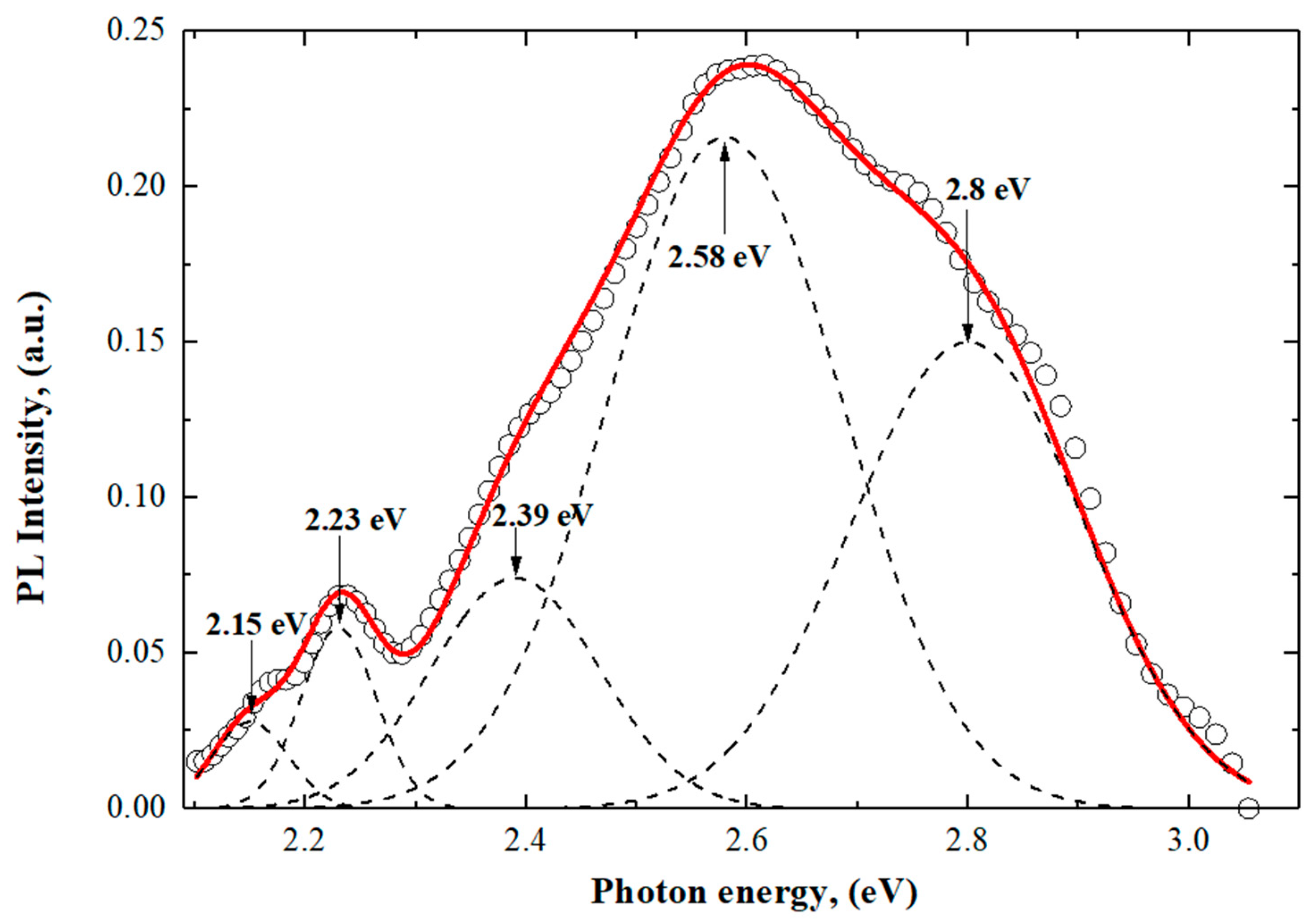
3.2. The Photoluminescence (PL) End Electrical Properties of Orthorhombic SnO2-NWs/SiO2/Si

Photoluminescence (PL) techniques are useful in detecting nanocrystal structure, defects, and impurities. Previous studies on the luminescence of SnO2 nanocrystals can be found in the following articles and references therein [60,61,62,63,64,65,66,67,68,69,70,71,72,73,74,75,76].
The PL of SnO2-NWs/SiO2/Si was investigated in the spectral range from 300 to 600 nm under excitation at λ = 240 nm. In Figure 5, the photoluminescence spectrum of SnO2-NWs/SiO2/Si structures is represented through Gaussian decomposition. We also subtracted the luminescence of amorphous silica.
The photoluminescence is caused by crystal defects or electronic transitions related to oxygen vacancies or interstitial tin, etc. They arise in the band gap during growth. Oxygen vacancies are the most common defects and usually act as emitting centers in luminescence processes. Oxygen vacancies are found in semiconductor oxides in three charge states: V O 0 , V O + and V O 2 + [70]. V O 0 is a very shallow donor; it corresponds to a peak of 2.39 eV (518.76 nm) [71], and most oxygen vacancies will be in the paramagnetic state V O + with peak at 2.58 eV (480 nm) [67,72]. The transition from the triplet state to the ground state for V O 0 may be associated with blue emission at a maximum of 2.8 eV (442.8 nm) [73]. Nanostructured SnO2 was found to have a similar observation in its PL spectrum [74]. The luminescence centers responsible for the maximum violet emission at 2.9 eV (427.53 nm) can be attributed to interstitial tin or tin with damaged bonds [65,66,67,68,69]. The peak at 2.15 eV (575 nm) is caused by trap emission from defect levels in the band gap, such as oxygen vacancies, rather than a direct electronic transition. In this SnO2-NWs/SiO2/Si nanoheterostructure, oxygen vacancies act as luminescent centers, forming defect levels that capture electrons from the valence band and contribute to luminescence [75,76]. It is probable that the observed peak of 2.23 eV (554 nm) is a result of oxygen vacancies that occur during deposition, as reported in studies [77,78]. Similar outcomes were discovered in the examination of SnO2 nanobelts [79] and beak-shaped nanorods [80]. It is widely understood that oxygen vacancies are the most frequent type of imperfection and often act as emitting defects in luminescence occurrences. Indeed, from the analysis of the PL spectrum, we can see that the dominant defects are oxygen vacancies, but not defects associated with Sn. This indicates oxygen deficiency. This deficiency can be explained by the electrochemical deposition conditions shown in Figure 6a.
On the inner walls of nanochannels in amorphous silicon dioxide there are silicon and oxygen ions and their vacancies. When an external electric field is applied, the top layer of silicon is charged negatively, and the created field prevents the free movement of oxygen radicals. At the same time, tin ions rush into the channel and interact with oxygen ions on the channel walls (amorphous SiO2) to form tin dioxide under conditions of oxygen deficiency, forming orthorhombic tin dioxide with various oxygen-vacancy defects. This also explains the low number of defects associated with tin.
To confirm the contact between SnO2 nanowires and silicon substrate, which can be clearly seen in Figure 6b, the current–voltage characteristics (CVCs) of the SnO2-NWs/SiO2/Si structure were investigated. To confirm the formation of junctions more clearly, a cross-sectional view is shown in Figure 7. It appears that SnO2 nanowires are tightly packed onto a silicon substrate and form junction structures. The CVCs were measured from an array of filled nanochannels with an area of 0.7 cm2. The CVCs were investigated using a second-order polynomial fitting [25].
Based on Figure 7, it is evident that the CVCs behave like a diode. This means that the current increases exponentially as the voltage increases in the forward direction. The current is attributed to electrons, as the Si substrate is of p-type. By analyzing the CVCs, it can be inferred that the SnO2-NWs/SiO2/Si structure has an electronic type of conductivity. We can determine the conductivity of nanowire arrays using Formula (1):
σ = d I d U   l A ,
where l is the length of the nanowire (approximately corresponds to the thickness of the oxide layer of the substrate, about 700 nm); A —area;   d I / d U —tangent of the angle of inclination I–U. Values for A = 2 π r 2 = 57174   nm 2 , σ = 1.5 × 10 8   Om 1 · cm 1 . Therefore, we can discuss the formation of a series of p-n junctions.
The conductivity of polycrystalline samples can be explained using diffusion and thermoemission models. When the barrier width W is much larger than the free path length of carriers L, we can use the diffusion theory. On the other hand, the thermoelectron emission model is applied when L > W. According to this model, only those carriers whose kinetic energy is greater than the barrier height can cross the boundary. If we assume that we have barriers of the same type, and on average a voltage of V/m is applied (where m is the number of barriers between the electrodes, and V is the interelectrode voltage), then we can use the following equation to determine the height of the potential barrier φ and the number of barriers m in series [81]:
I = I 0 exp e φ V m / k T ,
This equation is also used to analyze current transfer in polycrystalline gallium phosphite [82,83]. The number of barriers can be estimated using the Formula (3):
m =   H h k ,
where H is the height of the nanopore and hk is the linear size of the nanocrystallite. The average value of the lattice parameters from Table 2 can be used for hk.

4. Conclusions

We successfully obtained vertical nanowires of tin dioxide (SnO2) through electrochemical deposition into a SiO2/Si track template; they had an orthorhombic ZrO2 crystal structure with the lattice parameters a = 9.97195 Å, b = 5.11601 Å, and c = 5.03283 Å.
We calculated the band structure along the highly symmetric k-points of the Brillion zone along with the density of states. The lattice parameters of relaxed crystal geometry were also calculated and matched well with our experimental data. The maximum of the valence band and the bottom of the conduction band were located at the Г-point with a band gap of 3.76 eV, which had good agreement with previous studies.
The study of the PL spectrum showed a broad emission band in the spectral range of 400–600 nm, in which it was found that the dominant defects were oxygen vacancies. Also, maximums were found which were formed by interstitial tin or tin with damaged bonds.
Analysis of the CVCs of SnO2-NWs/SiO2/Si heterostructures with orthorhombic crystal structure showed that SnO2-NWs/SiO2/Si heterostructures with arrays of p-n junctions were synthesized.
Our proposed template synthesis method has several advantages over other methods. Firstly, it does not require lithography. Secondly, it allows for quick optimization of the template synthesis process. Lastly, it has potential applicability to various material systems.

Author Contributions

Conceptualization, V.K. and A.I.P.; methodology, A.D. and V.K.; software, A.U. and A.-D.B.; validation, Z.B., D.J. and A.A. (Aiman Akylbekova); formal analysis, V.K., A.A. (Abdirash Akilbekov) and A.I.P.; investigation, Z.B., D.J., A.A. (Aiman Akylbekova), G.B., G.A. and A.U.; resources, A.A. (Abdirash Akilbekov), G.A. and A.-D.B.; data curation, D.J.; writing—original draft preparation, Z.B., A.D., D.J., G.B., A.U. and A.I.P.; writing—review and editing, A.D.; visualization, G.B.; supervision, A.D. and A.A. (Abdirash Akilbekov); project administration, G.A.; funding acquisition, A.D. All authors have read and agreed to the published version of the manuscript.

Funding

This research was funded by the Ministry of Science and Higher Education of the Republic of Kazakhstan, grant number AP14871479 «Template synthesis and experimental-theoretical study of a new type of heterostructures for nano- and optoelectronic applications».

Data Availability Statement

Data are contained within the article.

Acknowledgments

The work was carried out within the framework of the grant project AP14871479 of the Ministry of Science and Higher Education of the Republic of Kazakhstan.

Conflicts of Interest

The authors declare no conflicts of interest.

References

  1. Lorenz, M.; Ramachandra Rao, M.S.; Venkatesan, T.; Fortunato, E.; Barquinha, P.; Branquinho, R. Topical Review: The oxide electronic materials and oxide interfaces roadmap. J. Phys. D Appl. Phys. 2016, 49, 433001. [Google Scholar] [CrossRef]
  2. Varghese, B.; Hoong, T.C.; Yanwu, Z.; Reddy, M.V.; Chowdari, B.V.R.; Wee, A.T.S.; Vincent, T.B.C.; Lim, C.T.; Sow, C.H. Co3O4 nanostructures with different morphologies and their field-emission properties. Adv. Funct. Mater. 2007, 17, 1932–1939. [Google Scholar] [CrossRef]
  3. Fang, X.S.; Yan, J.; Hu, L.F.; Liu, H.; Lee, P.S. Thin SnO2 nanowires with uniform diameter as excellent field emitters: A stability of more than 2400 minutes. Adv. Funct. Mater. 2012, 22, 1613–1622. [Google Scholar] [CrossRef]
  4. Bie, Y.Q.; Liao, Z.M.; Zhang, H.Z.; Li, G.R.; Ye, Y.; Zhou, Y.B.; Xu, J.; Qin, Z.X.; Dai, L.; Yu, D.P. Self-powered, ultrafast, visible-blind UV detection and optical logical operation based on ZnO/GaN nanoscale p-n junctions. Adv. Funct. Mater. 2011, 23, 649–653. [Google Scholar] [CrossRef] [PubMed]
  5. Rigutti, L.; Tchernycheva, M.; Bugallo, A.D.; Jacopin, G.; Julien, F.H.; Zagonel, L.F.; March, K.; Stephan, O.; Kociak, M.; Songmuang, R. Ultraviolet photodetector based on GaN/AlN quantum discs in a single nanowire. Nano Lett. 2010, 10, 2939–2943. [Google Scholar] [CrossRef] [PubMed]
  6. Tang, J.S.; Wang, C.Y.; Xiu, F.X.; Lang, M.R.; Chu, L.W.; Tsai, C.J.; Chueh, Y.L.; Chen, L.J.; Wang, K.L. Oxide-confined formation of germanium nanowire heterostructures for high-performance transistors. Am. Chem. Soc. Nano 2011, 5, 6008–6015. [Google Scholar] [CrossRef] [PubMed]
  7. Kulmala, T.S.; Colli, A.; Fasoli, A.; Lombardo, A.; Haque, S.; Ferrari, A.C. Self-Aligned coupled nanowire. Am. Chem. Soc. Nano 2011, 5, 6910–6915. [Google Scholar] [CrossRef]
  8. Vaseashta, A.; Dimova-Malinovska, D. Nanostructured and nanoscale devices, sensors and detectors. Sci. Technol. Adv. Mater. 2005, 6, 312–318. [Google Scholar] [CrossRef]
  9. Chou, J.C.; Wang, Y.F. Preparation and study on the drift and hysteresis properties of the tin oxide gate ISFET by the sol-gel method. Sens. Actuators B Chem. 2002, 86, 58–62. [Google Scholar] [CrossRef]
  10. Lee, J.S.; Sim, S.K.; Min, B.; Cho, K.; Kim, S.W.; Kim, S. Structural and optoelectronic properties of SnO2 nanowires synthesized from ball-milled SnO2 powders. J. Cryst. Growth 2004, 267, 145–149. [Google Scholar] [CrossRef]
  11. Ying, Z.; Wan, Q.; Song, Z.T.; Feng, S.L. Controlled synthesis of branched SnO2 nanowhiskers. Mater. Lett. 2005, 59, 1670–1672. [Google Scholar] [CrossRef]
  12. Fan, Y.; Liu, J.; Lu, H. Hierarchical structure SnO2 supported Pt nanoparticles as enhanced electrocatalyst for methanol oxidation. Electrochim. Acta 2012, 76, 475–479. [Google Scholar] [CrossRef]
  13. Heiss, M.; Fontana, Y.; Gustafsson, A.; Wust, G.; Magen, C.; O’Regan, D.; Luo, J.; Ketterer, B.; Conesa-Boj, S.; Kuhlmann, A.; et al. Self-assembled quantum dots in a nanowire system for quantum photonics. Nat. Mater. 2013, 12, 439–444. [Google Scholar] [CrossRef]
  14. Kozlovskii, A.L.; Kadyrzhanov, K.K.; Zdorovets, M.V. Structural and Conductive Characteristics of Fe/Co Nanotubes. Russ. J. Electrochem. 2018, 54, 178–185. [Google Scholar] [CrossRef]
  15. Kozlovskiy, A.; Zhanbotin, A.; Zdorovets, M.; Manakova, I.; Ozernoy, A.; Kadyrzhanov, K.; Rusakov, V. Study of Ni/Fe nanotube properties. Nucl. Instrum. Methods Phys. Res. Sect. B Beam Interact. Mater. At. 2015, 365, 663–667. [Google Scholar] [CrossRef]
  16. Mashentseva, A.; Borgekov, D.; Kislitsin, S.; Sdorovets, M.; Migunova, A. Comparative catalytic activity of PET track-etched membranes with embedded silver and gold nanotubes. Nucl. Instrum. Methods Phys. Res. Sect. B Beam Interact. Mater. At. 2015, 365, 70–74. [Google Scholar] [CrossRef]
  17. Demyanov, S.; Kaniukov, E.; Petrov, A.; Sivakov, V. Positive magnetoresistive effect in Si/SiO2 (Cu/Ni) nanostructures. Sens. Actuators A Phys. 2014, 216, 64–68. [Google Scholar] [CrossRef]
  18. Sivakov, V.; Kaniukov, E.Y.; Petrov, A.; Korolik, O.; Mazmanik, A.; Bochmann, A.; Teichert, S.; Hidi, I.J.; Schleusener, A.; Gialla, D.; et al. Novel silver nanostructures formation in porous Si/SiO2 matrix. J. Cryst. Growth 2014, 400, 21–26. [Google Scholar] [CrossRef]
  19. Fertig, N.; Blick, R.H.; Behrends, J.C. Whole cell patch clamp recording performed on a planar glass chip. Biophys. J. 2002, 82, 3056–3062. [Google Scholar] [CrossRef]
  20. Hoppe, K.; Fahrner, W.R.; Fink, D.; Dhamodoran, S.; Petrov, A.; Chandra, A.; Saad, A.; Faupel, F.; Chakravadhanula, V.S.K.; Zaporotchenko, V. An ion track based approach to nano-and micro-electronics. Nucl. Instrum. Methods Phys. Res. Sect. B Beam Interact. Mater. At. 2008, 266, 1642–1646. [Google Scholar] [CrossRef]
  21. Kaniukov, E.; Bundyukova, V.; Kutuzau, M.; Yakimchuk, A. Preculiarities of Formation and Characterization of SiO2/Si Ion-Track Template. In Fundamental and Applied Nano-Electromagnetics II: THz Circuits, Materials, Devices; Springer: Dordrecht, The Netherlands, 2019; pp. 41–57. [Google Scholar] [CrossRef]
  22. Dallanora, A.; Marcondes, T.L.; Bermudez, G.G.; Fichtner, P.F.P.; Trautman, C.; Toulemonde, M.; Papaleo, R.M. Nanoporous SiO2/Si thin layers produced by ion track etching: Dependence on the ion energy and criterion for etchability. J. Appl. Phys. 2008, 104, 024307. [Google Scholar] [CrossRef]
  23. Giniyatova, S.; Dauletbekova, A.; Baimukhanov, Z.; Vlasukova, L.; Akilbekov, A. Structure, electrical properties and lum. of ZnO NCs deposited in SiO2/Si track templates. Radiat. Meas. 2019, 125, 52–56. [Google Scholar] [CrossRef]
  24. Balakhayeva, R.; Akilbekov, A.; Baimukhanov, Z.; Giniyatova, S.; Zdorovets, M.; Gorin, Y.; Popov, A.I.; Dauletbekova, A. Structure properties of CdTe nanocrystals created in SiO2/Si ion track templates. Surf. Coat. Technol. 2020, 401, 126269. [Google Scholar] [CrossRef]
  25. Dauletbekova, A.; Akylbekova, A.; Sarsekhan, G.; Usseinov, A.; Baimukhanov, Z.; Kozlovskiy, A.; Vlasukova, L.A.; Komarov, F.F.; Popov, A.I.; Akilbekov, A.T. Ion-track template synthesis and characterization of ZnSeO3 Nanocrystals. Crystals 2022, 12, 817. [Google Scholar] [CrossRef]
  26. Dovesi, R.; Erba, A.; Orlando, R.; Zicovich-Wilson, C.M.; Civalleri, B.; Maschio, L.; Rérat, M.; Casassa, S.; Baima, J.; Salustro, S.; et al. Quantum-mechanical condensed matter simulations with CRYSTAL. Wiley Interdiscip. Rev. Comput. Mol. Sci. 2018, 8, e1360. [Google Scholar] [CrossRef]
  27. Dauletbekova, A.K.; Alzhanova, A.Y.; Akilbekov, A.T.; Mashentseva, A.A.; Zdorovets, M.V.; Balabekov, K.N. Synthesis of Si/SiO2/ZnO nanoporous materials using chemical and electrochemical deposition techniques. In AIP Conference Proceedings; AIP Publishing LLC: Melville, NY, USA, 2016; Volume 1767, p. 020005. [Google Scholar] [CrossRef]
  28. Laun, J.; Bredow, T. BSSE-corrected consistent Gaussian basis sets of triple-zeta valence with polarization quality of the fifth period for solid-state calculations. J. Comput. Chem. 2022, 12, 839–846. [Google Scholar] [CrossRef] [PubMed]
  29. Vilela Oliveira, D.; Peintinger, M.F.; Laun, J.; Bredow, T. BSSE-correction scheme for consistent gaussian basis sets of double-and triple-zeta valence with polarization quality for solid-state calculations. J. Comput. Chem. 2019, 27, 2364–2376. [Google Scholar] [CrossRef] [PubMed]
  30. Becke, A.D. Density-Functional Thermochemistry. III. The Role of Exact Exchange. J. Chem. Phys. 1993, 98, 5648–5652. [Google Scholar] [CrossRef]
  31. Lee, C.; Yang, W.; Parr, R.G. Development of the Colic-Salvetti correlation-energy formula into a Functional of the Electron Density. Phys. Rev. B 1998, 37, 785–789. [Google Scholar] [CrossRef] [PubMed]
  32. Mulliken, R.S. Electronic population analysis on LCAO–MO molecular wave functions. II. Overlap populations, bond orders, and covalent bond energies. J. Chem. Phys. 1955, 23, 1841–1846. [Google Scholar] [CrossRef]
  33. Slassi, A.; Hammi, M.; Oumekloul, Z.; Nid-bahami, A.; Arejdal, M.; Ziat, Y.; El Rhazouani, O. Effect of halogens doping on transparent conducting properties of SnO2 rutile: An ab initio investigation. Opt. Quantum Electron. 2018, 50, 8. [Google Scholar] [CrossRef]
  34. Balakrishnan, K.; Veerapandy, V.; Fjellvag, V.; Vajeeston, P. First-principles exploration into the physical and chemical properties of certain newly identified SnO2 polymorphs. ACS Omega 2022, 12, 10382–10393. [Google Scholar] [CrossRef]
  35. Arlinghaus, F.J. Energy bands in stannic oxide (SnO2). J. Phys. Chem. Solids 1974, 8, 931–935. [Google Scholar] [CrossRef]
  36. Barbarat, P.; Matar, S.F. First-principles investigations of the electronic, optical and chemical bonding properties of SnO2. Comput. Mater. Sci. 1998, 1–4, 368–372. [Google Scholar] [CrossRef]
  37. Kucheyev, S.O.; Baumann, T.F.; Sterne, P.A.; Wang, Y.M.; van Buuren, T.; Hamza, A.V.; Terminello, L.J.; Willey, T.M. Surface electronic states in three-dimensional SnO2 nanostructures. Phys. Rev. B 2005, 3, 035404. [Google Scholar] [CrossRef]
  38. Nagasawa, M.; Shionoya, S. Temperature dependence of the fundamental optical absorption edge in stannic oxide. J. Phys. Soc. Jpn. 1971, 4, 1118–1123. [Google Scholar] [CrossRef]
  39. Themlin, J.M.; Sporken, R.; Darville, K.; Caudano, R.; Gilles, J.M.; Johnson, R.L. Resonant-photoemission study of SnO2: Cationic origin of the defect band-gap states. Phys. Rev. B 1990, 18, 11914. [Google Scholar] [CrossRef] [PubMed]
  40. Maki-Jaskari, M.A.; Rantala, T.T. Band structure and optical parameters of the SnO2 (110) surface. Phys. Rev. B 2001, 7, 075407. [Google Scholar] [CrossRef]
  41. Suito, K.; Kawai, N.; Masuda, Y. High pressure synthesis of orthorhombic SnO2. Mater. Res. Bull. 1975, 10, 677–680. [Google Scholar] [CrossRef]
  42. Shieh, S.R.; Kubo, A.; Duffy, T.S.; Prakapenka, V.B.; Shen, G. High-pressure phases in SnO2 to 117 GPa. Phys. Rev. B 2006, 73, 014105. [Google Scholar] [CrossRef]
  43. Chen, Z.; Lai, J.K.L.; Shek, C.H. Facile strategy and mechanism for orthorhombic SnO2 thin films. Appl. Phys. Lett. 2006, 89, 231902. [Google Scholar] [CrossRef]
  44. Kaplan, L.; Ben-Shalom, A.; Boxman, R.L.; Goldsmith, S.; Rosenberg, U.; Nathan, M. Annealing and Sb-doping of Sn—O films produced by filtered vacuum arc deposition: Structure and electro-optical properties. Thin Solid Film. 1994, 253, 1–8. [Google Scholar] [CrossRef]
  45. Lamelas, F.J.; Reid, S.A. Thin-film synthesis of the orthorhombic phase of SnO2. Phys. Rev. B 1999, 60, 9347. [Google Scholar] [CrossRef]
  46. Bae, J.Y.; Park, J.; Kim, H.Y.; Kim, H.S.; Park, J.S. Facile route to the controlled synthesis of tetragonal and orthorhombic SnO2 films by mist chemical vapor deposition. ACS Appl. Mater. Interfaces 2015, 7, 12074–12079. [Google Scholar] [CrossRef] [PubMed]
  47. Mueller, E. RHEED-Untersuchungen einer grenzschichtstruktur von SnO2 auf quarz. Acta Crystallogr. Sect. B Struct. Sci. 1984, 40, 359–363. [Google Scholar] [CrossRef]
  48. Sangaletti, L.; Depero, L.E.; Dieguez, A.; Marca, G.; Morante, J.R.; Romano-Rodriguez, A.; Sberveglieri, G. Microstructure and morphology of tin dioxide multilayer thin film gas sensors. Sens. Actuators B Chem. 1997, 44, 268–274. [Google Scholar] [CrossRef]
  49. Sberveglieri, G.; Faglia, G.; Groppelli, S.; Nelli, P.; Taroni, A. A novel PVD technique for the preparation of SnO2 thin films as C2H5OH sensors. Sens. Actuators B Chem. 1992, 7, 721–726. [Google Scholar] [CrossRef]
  50. Masuda, Y. Recent advances in SnO2 nanostructure based gas sensors. Sens. Actuators B Chem. 2022, 364, 131876. [Google Scholar] [CrossRef]
  51. Lu, S.; Zhang, Y.; Liu, J.; Li, H.; Hu, Z.; Luo, X.; Gao, N.; Zhang, B.; Jiang, J.; Zhong, A.; et al. Sensitive H2 gas sensors based on SnO2 nanowires. Sens. Actuators B Chem. 2021, 345, 130334. [Google Scholar] [CrossRef]
  52. Park, H.; Kim, J.; Vivod, D.; Kim, S.; Mirzaei, A.; Zahn, D.; Park, C.; Kim, S.S.; Halik, M. Chemical-recognition-driven selectivity of SnO2-nanowire-based gas sensors. Nano Today 2021, 40, 101265. [Google Scholar] [CrossRef]
  53. Sharma, A.; Khosla, A.; Arya, S. Synthesis of SnO2 nanowires as a reusable and flexible electrode for electrochemical detection of riboflavin. Microchem. J. 2020, 156, 104858. [Google Scholar] [CrossRef]
  54. Dai, Z.R.; Gole, J.L.; Stout, J.D.; Wang, Z.L. Tin oxide nanowires, nanoribbons, and nanotubes. J. Phys. Chem. B 2002, 106, 1274–1279. [Google Scholar] [CrossRef]
  55. Dai, Z.R.; Pan, Z.W.; Wang, Z.L. Novel nanostructures of functional oxides synthesized by thermal evaporation. Adv. Funct. Mater. 2003, 13, 9–24. [Google Scholar] [CrossRef]
  56. Ihn, S.G.; Song, J.I.; Kim, T.W.; Leem, D.S.; Lee, T.; Lee, S.G.; Koh, E.K.; Song, K. Morphology-and orientation-controlled gallium arsenide nanowires on silicon substrates. Nano Lett. 2007, 7, 39–44. [Google Scholar] [CrossRef]
  57. Arbiol, J.; Kalache, B.; Roca i Cabarrocas, P.; Morante, J.R.; Fontcuberta i Morral, A. Influence of Cu as a catalyst on the properties of silicon nanowires synthesized by the vapour–solid–solid mechanism. Nanotechnology 2007, 18, 305606. [Google Scholar] [CrossRef]
  58. Dauletbekova, A.; Vlasukova, L.; Baimukhanov, Z.; Akilbekov, A.; Kozlovskiy, A.; Giniyatova, S.; Seitbayev, A.; Usseinov, A.; Akylbekova, A. Synthesis of ZnO Nanocrystals in SiO2/Si Track Template: Effect of Electrodeposition Parameters on Structure. Phys. Status Solidi B 2019, 256, 1800408. [Google Scholar] [CrossRef]
  59. Arbiol, J.; Comini, E.; Faglia, G.; Sberveglieri, G.; Morante, J.R. Orthorhombic Pbcn SnO2 nanowires for gas sensing applications. J. Cryst. Growth 2008, 310, 253–260. [Google Scholar] [CrossRef]
  60. Gu, F.; Wang, S.F.; Lu, M.K.; Zhou, G.J.; Xu, D.; Yuan, D.R. Photoluminescence properties of SnO2 nanoparticles synthesized by sol−gel method. J. Phys. Chem. B 2004, 108, 8119–8123. [Google Scholar] [CrossRef]
  61. Chowdhury, P.S.; Saha, S.; Patra, A. Influence of nanoenvironment on luminescence of Eu3+ activated SnO2 nanocrystals. Solid State Commun. 2004, 131, 785–788. [Google Scholar] [CrossRef]
  62. Faglia, G.; Baratto, C.; Sberveglieri, G.; Zha, M.; Zappettini, A. Adsorption effects of NO2 at ppm level on visible photoluminescence response of SnO2 nanobelts. Appl. Phys. Lett. 2005, 86, 011923. [Google Scholar] [CrossRef]
  63. Maestre, D.; Cremades, A.; Piqueras, J. Growth and luminescence properties of micro-and nanotubes in sintered tin oxide. J. Appl. Phys. 2005, 97, 044316. [Google Scholar] [CrossRef]
  64. Gu, F.; Wang, S.F.; Song, C.F.; Lu, M.K.; Qi, Y.X.; Zhou, G.J.; Xu, D.; Yuan, D.R. Synthesis and luminescence properties of SnO2 nanoparticles. Chem. Phys. Lett. 2003, 372, 451–454. [Google Scholar] [CrossRef]
  65. Munnix, S.; Schmeits, M. Electronic structure of tin dioxide surfaces. Phys. Rev. B 1983, 27, 7624. [Google Scholar] [CrossRef]
  66. Chiodini, N.; Paleari, A.; DiMartino, D.; Spinolo, G. SnO2 nanocrystals in SiO2: A wide-band-gap quantum-dot system. Appl. Phys. Lett. 2002, 81, 1702–1704. [Google Scholar] [CrossRef]
  67. Vanheusden, K.; Warren, W.L.; Seager, C.H.; Tallant, D.R.; Voigt, J.A.; Gnade, B.E. Mechanisms behind green photoluminescence in ZnO phosphor powders. J. Appl. Phys. 1996, 79, 7983–7990. [Google Scholar] [CrossRef]
  68. Liu, Y.; Yang, Q.; Xu, C. Single-narrow-band red upconversion fluorescence of ZnO nanocrystals codoped with Er and Yb and its achieving mechanism. J. Appl. Phys. 2008, 104, 064701. [Google Scholar] [CrossRef]
  69. Godinho, K.G.; Walsh, A.; Watson, G.W. Energetic and electronic structure analysis of intrinsic defects in SnO2. J. Phys. Chem. C 2009, 113, 439–448. [Google Scholar] [CrossRef]
  70. Zhang, W.F.; Zhang, M.S.; Yin, Z.; Chen, Q. Photoluminescence in anatase titanium dioxide nanocrystals. Appl. Phys. B 2000, 70, 261–265. [Google Scholar] [CrossRef]
  71. Bhatnagar, M.; Kaushik, V.; Kaushal, A.; Singh, M.; Mehta, B. Structural and photoluminescence properties of tin oxide and tin oxide: C core–shell and alloy nanoparticles synthesised using gas phase technique. AIP Adv. 2016, 6, 095321. [Google Scholar] [CrossRef]
  72. Rani, S.; Roy, S.; Karar, N.; Bhatnagar, M. Structure, microstructure and photoluminescence properties of Fe doped SnO2 thin films. Solid State Commun. 2007, 141, 214–218. [Google Scholar] [CrossRef]
  73. Her, Y.C.; Wu, J.Y.; Lin, Y.R.; Tsai, S.Y. Low-temperature growth and blue luminescence of SnO2 nanoblades. Appl. Phys. Lett. 2006, 89, 043115. [Google Scholar] [CrossRef]
  74. Hu, J.Q.; Bando, Y.; Golberg, D. Self-catalyst growth and optical properties of novel SnO2 fishbone-like nanoribbons. Chem. Phys. Lett. 2003, 372, 758–762. [Google Scholar] [CrossRef]
  75. Cai, D.; Su, Y.; Chen, Y.; Jiang, J.; He, Z.; Chen, L. Synthesis and photoluminescence properties of novel SnO2 asterisk-like nanostructures. Mater. Lett. 2005, 59, 1984–1988. [Google Scholar] [CrossRef]
  76. Sinha, S.K.; Bhattacharya, R.; Ray, S.K.; Manna, I. Influence of deposition temperature on structure and morphology of nanostructured SnO2 films synthesized by pulsed laser deposition. Mater. Lett. 2011, 65, 146–149. [Google Scholar] [CrossRef]
  77. Duan, J.; Gong, J.; Huang, H.; Zhao, X.; Cheng, G.; Yu, Z.; Yang, S. Multiform structures of SnO2 nanobelts. Nanotechnology 2007, 18, 055607. [Google Scholar] [CrossRef]
  78. Zhang, L.; Ge, S.; Zuo, Y.; Zhang, B.; Xi, L. Influence of oxygen flow rate on the morphology and magnetism of SnO2 nanostructures. J. Phys. Chem. C 2010, 114, 7541–7547. [Google Scholar] [CrossRef]
  79. Hu, J.Q.; Bando, Y.; Liu, Q.L.; Golberg, D. Laser-ablation growth and optical properties of wide and long single-crystal SnO2 ribbons. Adv. Funct. Mater. 2003, 13, 493–496. [Google Scholar] [CrossRef]
  80. He, J.H.; Wu, T.H.; Hsin, C.L.; Li, K.M.; Chen, L.J.; Chueh, Y.L.; Chou, L.J.; Wang, Z.L. Beaklike SnO2 nanorods with strong photoluminescent and field-emission properties. Small 2006, 2, 116–120. [Google Scholar] [CrossRef] [PubMed]
  81. Touskova, J.; Tousek, J.; Klier, E.; Kuzel, R. Preparation and basic electrical properties of CdTe thick films. Phys. Status Solidi 1979, 56, 315–322. [Google Scholar] [CrossRef]
  82. Davis, E.A. States in the gap and defects in amorphous semiconductors. Amorph. Semicond. 2005, 36, 41–72. [Google Scholar] [CrossRef]
  83. Belyaev, A.P.; Rubets, V.P.; Nuzhdin, M.Y. Electrical properties of cadmium telluride films synthesized in a thermal field with a temperature gradient. Semiconductors 2003, 37, 646–648. [Google Scholar] [CrossRef]
Figure 1. SEM image of the n-type template surface after ECD at 1.75 V for 10 min.
Materials 17 01226 g001
Figure 2. X-ray diffractogram of samples obtained by the ECD for 10 min, at U = 1.75 V.
Materials 17 01226 g002
Figure 3. Band structure and total density of states of pure SnO2 crystal. The green dotted lines mark the band edges that separate the 3.76 eV bandgap. The Fermi level corresponds to 0 eV.
Materials 17 01226 g003
Figure 4. The SnO2 polymorph with ZrO2-type (Pbca) structure.
Materials 17 01226 g004
Figure 5. The photoluminescence spectrum of SnO2-NWs/SiO2/Si structures is decomposed into Gaussian components; SiO2 luminescence is taken into account in the PL spectrum.
Materials 17 01226 g005
Figure 6. (a) Preparation of orthorhombic SnO2 nanowires by ECD in SiO2/Si and (b) the cross-section of filled template.
Materials 17 01226 g006
Figure 7. Current–voltage characteristics of SnO2-NWs/SiO2/Si: dashed curve—initial sample; solid curve—with precipitated SnO2 (tdeposition = 10 min).
Materials 17 01226 g007
Table 1. Crystallographic characteristics of SnO2 nanowires in SiO2/Si (-p) track template according to XRD results. The calculated parameters are presented in parentheses.
Phase NameStructure TypeSpace Group(hkl)d, ÅL, nmFWHMCell Parameters, ÅVolume, Å3Density, g/cm3Degree of Crystallinity, %Phase Content, %
SnO2OrthorhombicPbca (61)20240.2192.2404619.390.485a = 9.97195
(10.05)
b = 5.11601
(5.10)
c = 5.03283
(5.18)
256.76
(266.26)
7.819
(7.57)
41.8100
Table 2. Parameters of intercrystalline barriers in SnO2 nanocrystallites.
H, nmT, Kmhk, ÅBarrier Height E, eV
70030010446.73.82 × 10−2
Disclaimer/Publisher’s Note: The statements, opinions and data contained in all publications are solely those of the individual author(s) and contributor(s) and not of MDPI and/or the editor(s). MDPI and/or the editor(s) disclaim responsibility for any injury to people or property resulting from any ideas, methods, instructions or products referred to in the content.

