
Physical Characteristics of Sintered Silver Nanoparticle Inks with Different Sizes during Furnace Sintering

 , and
, and
Abstract
1. Introduction
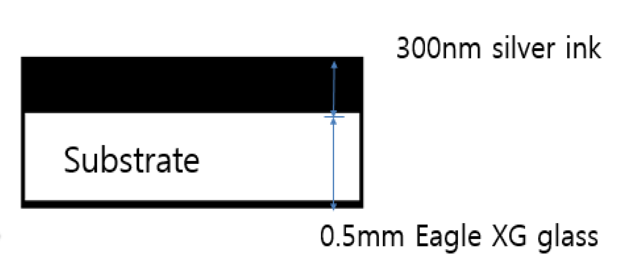
2. Experimental Methods
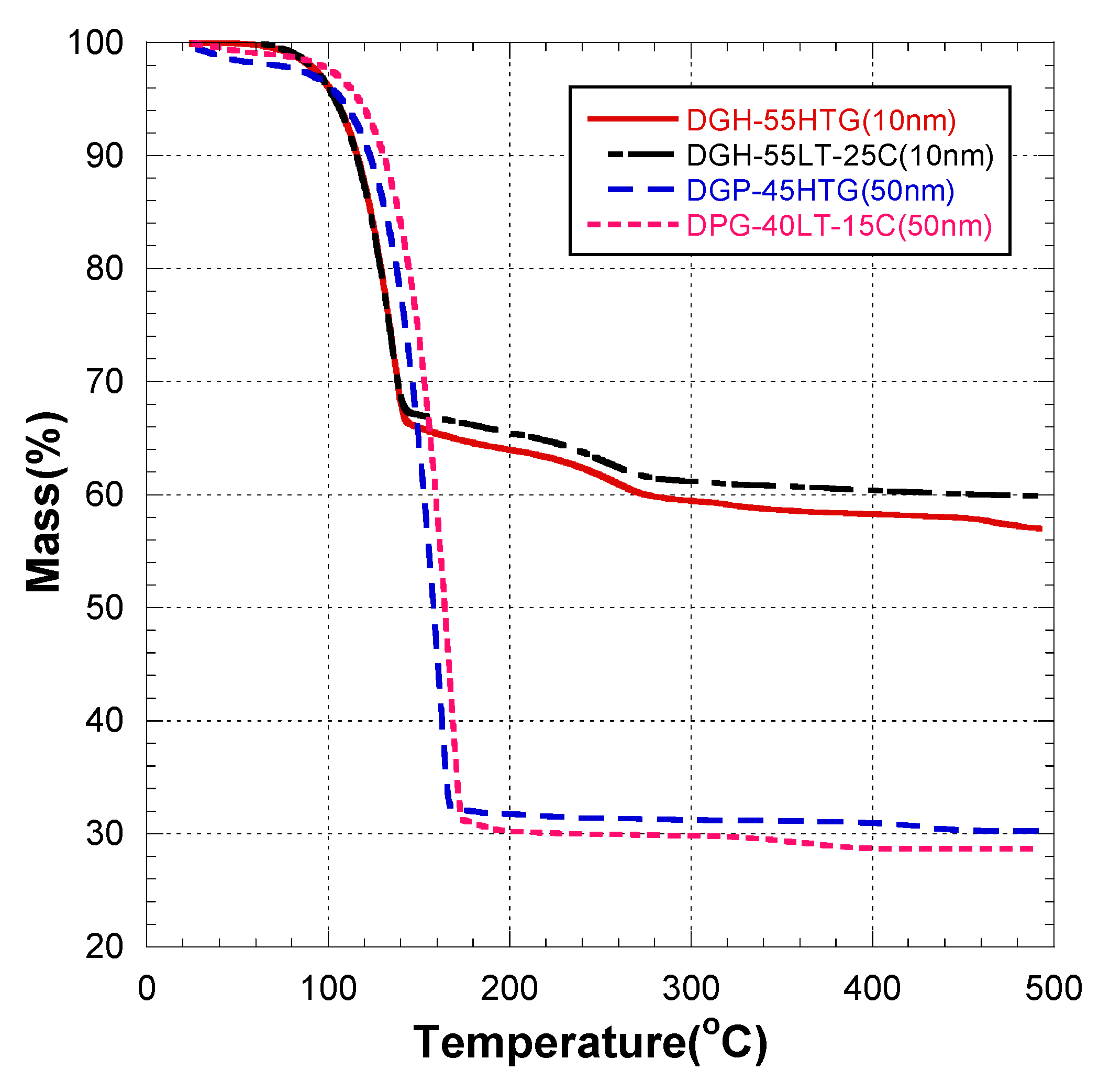
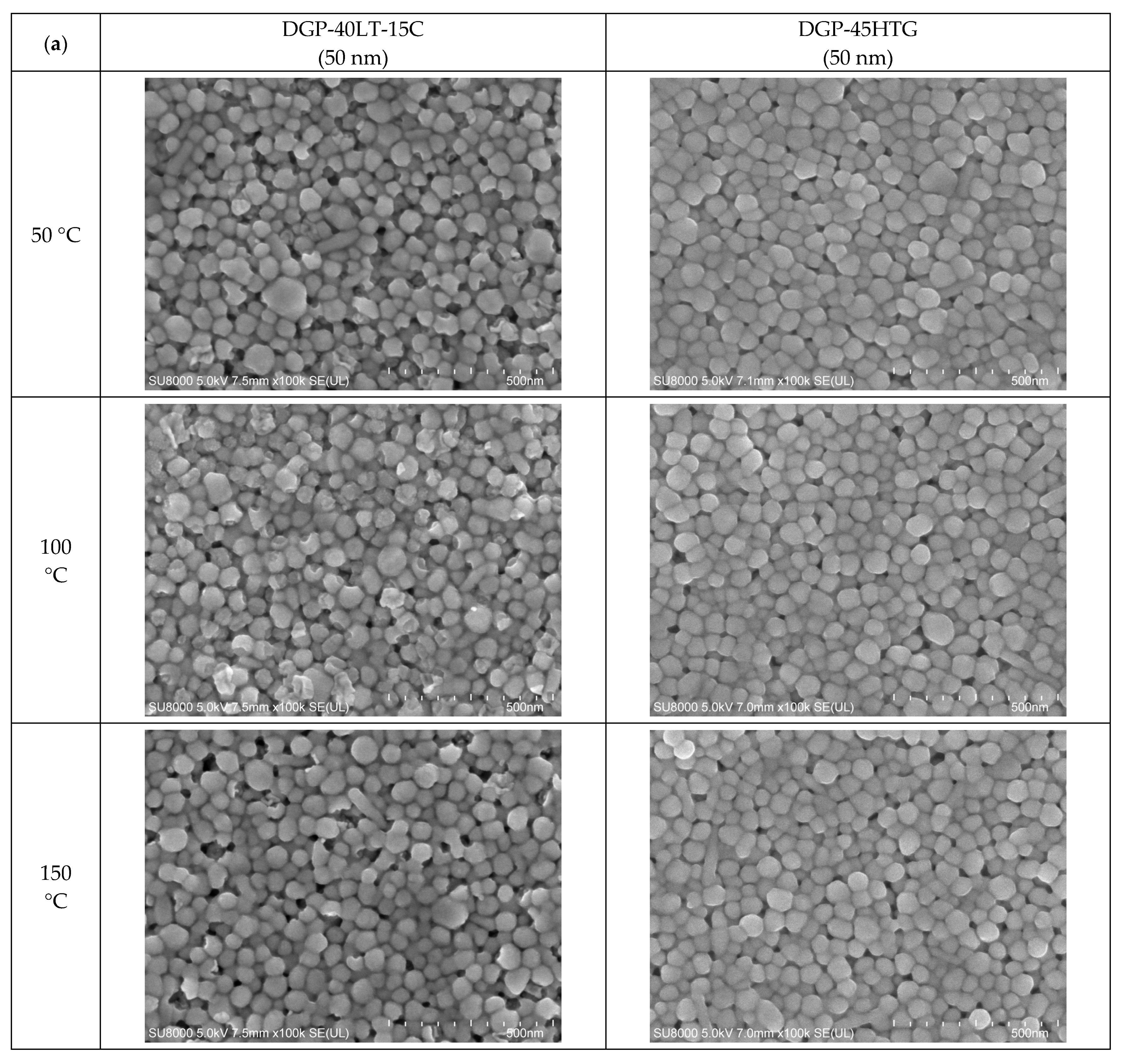
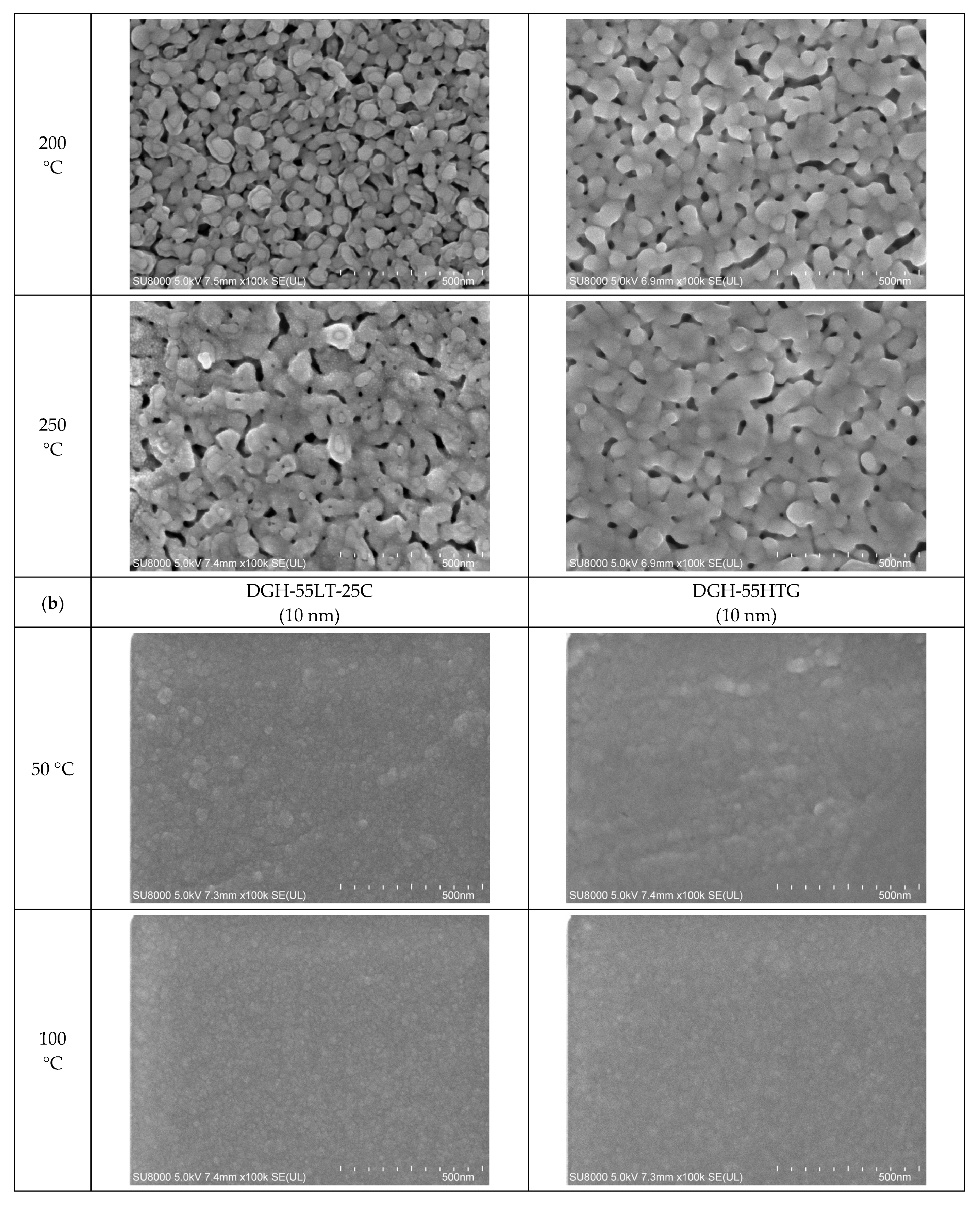
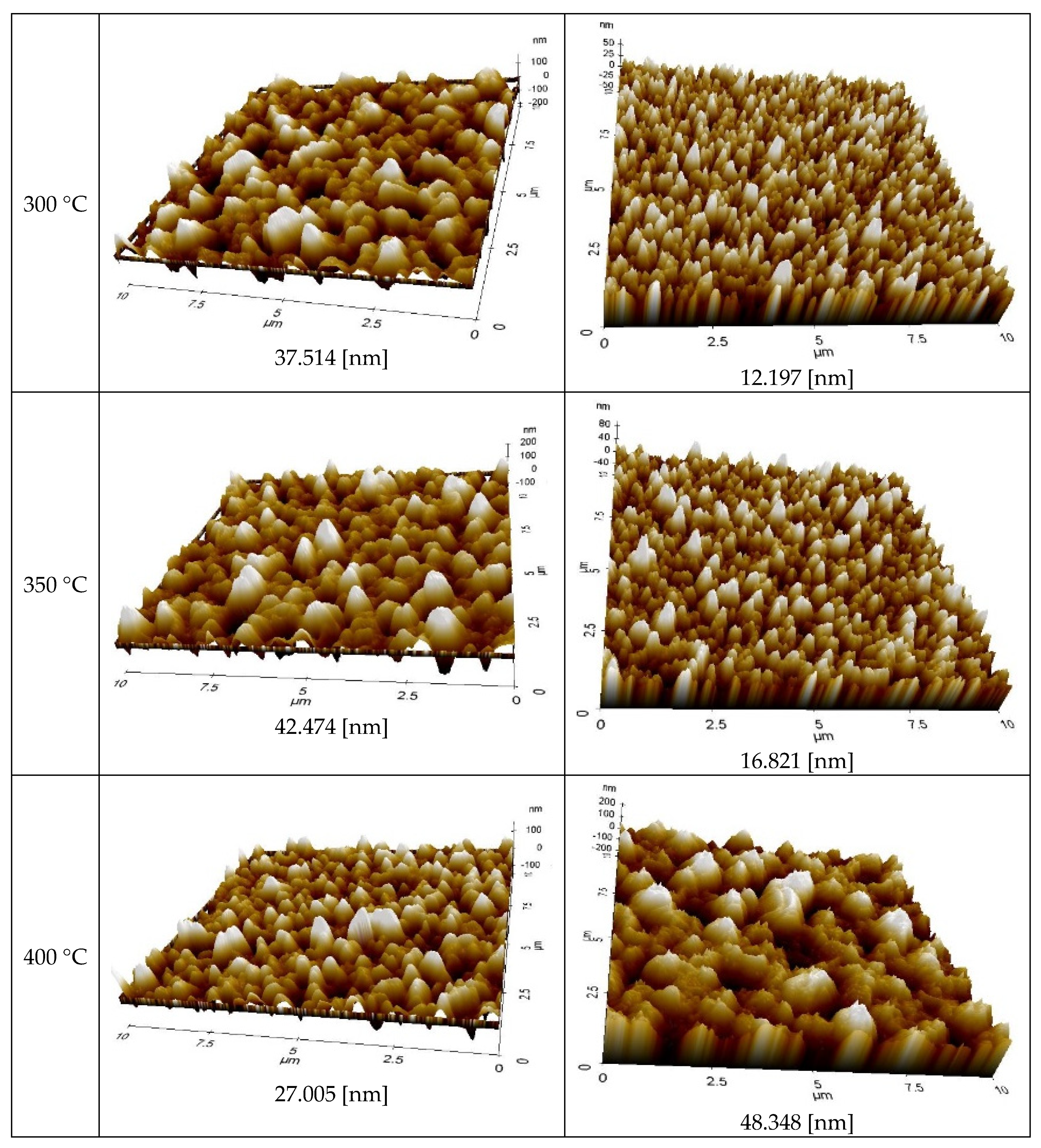
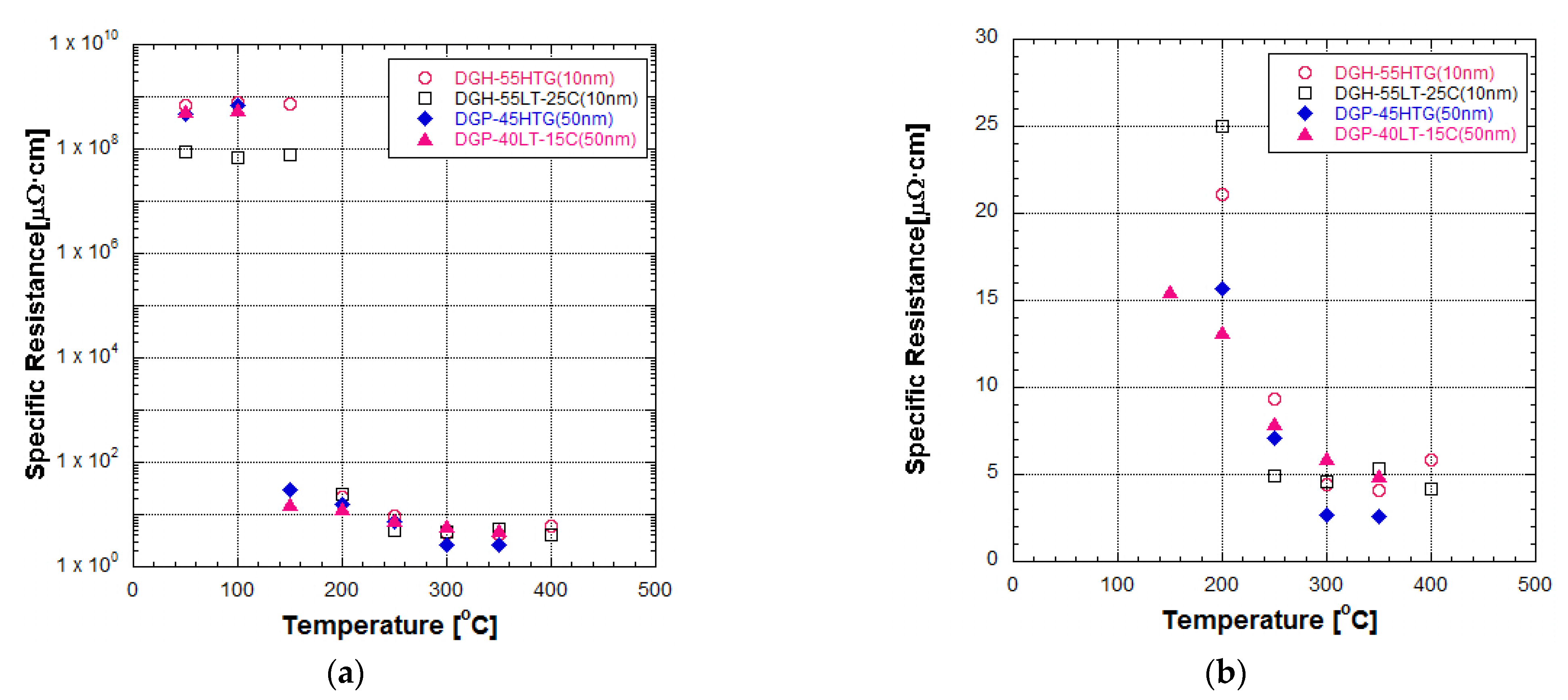
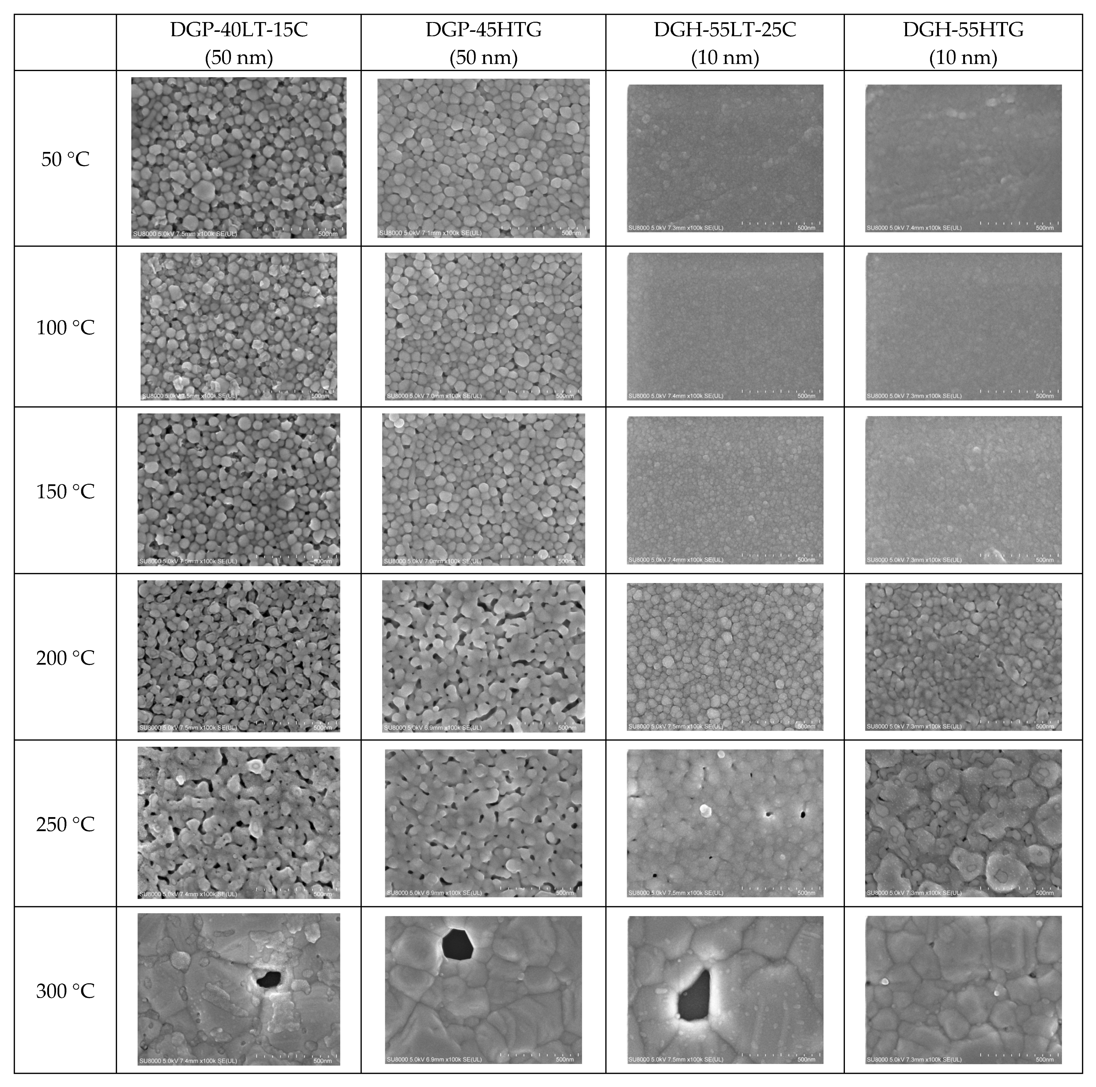
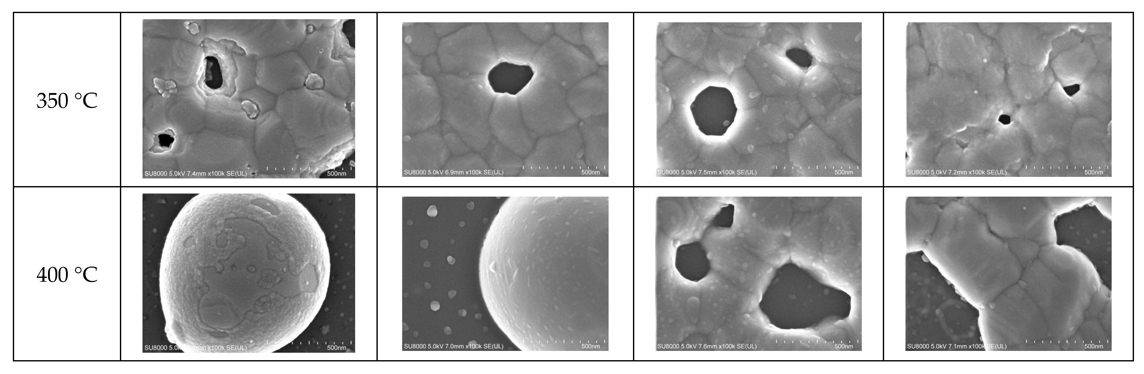
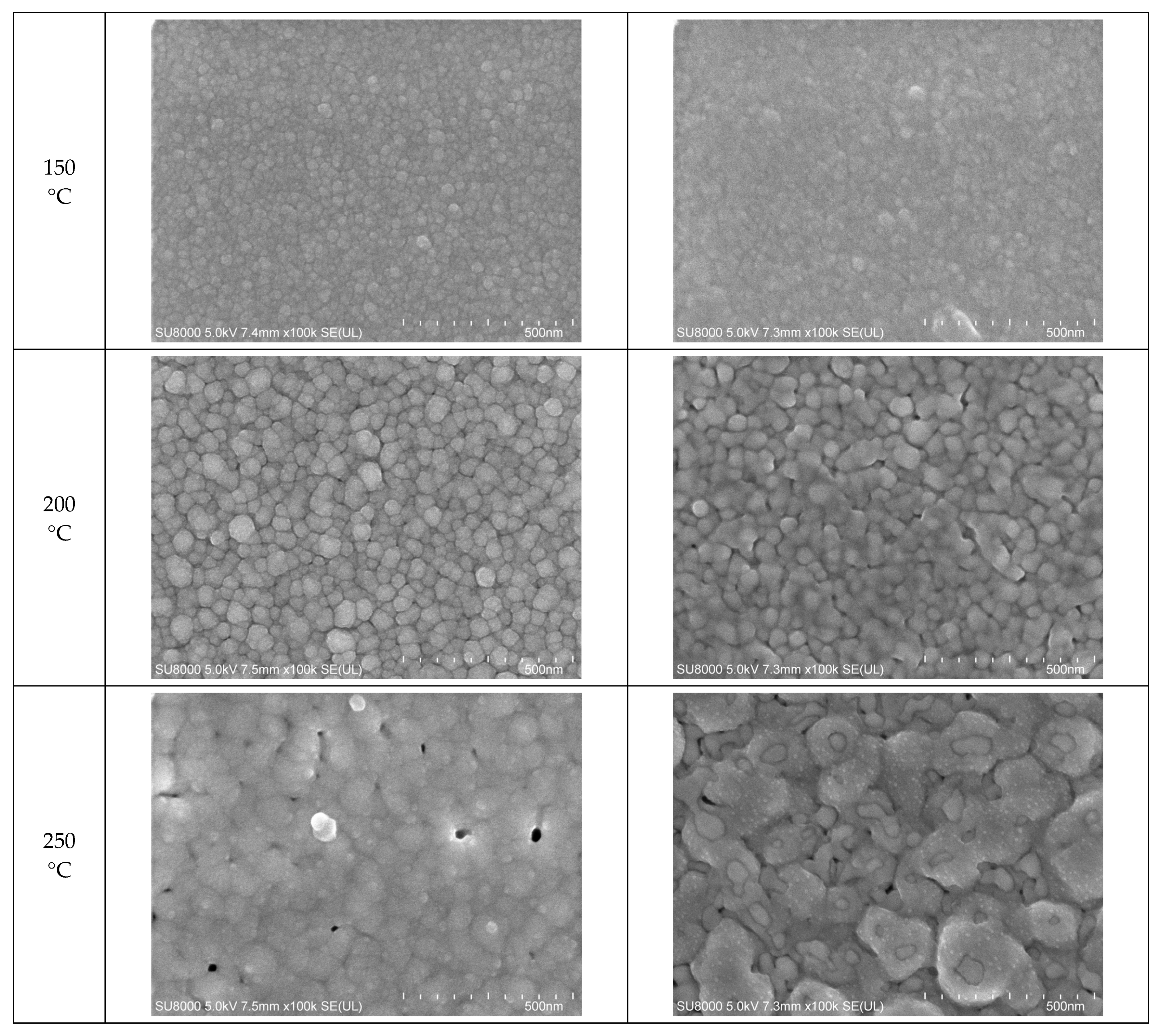
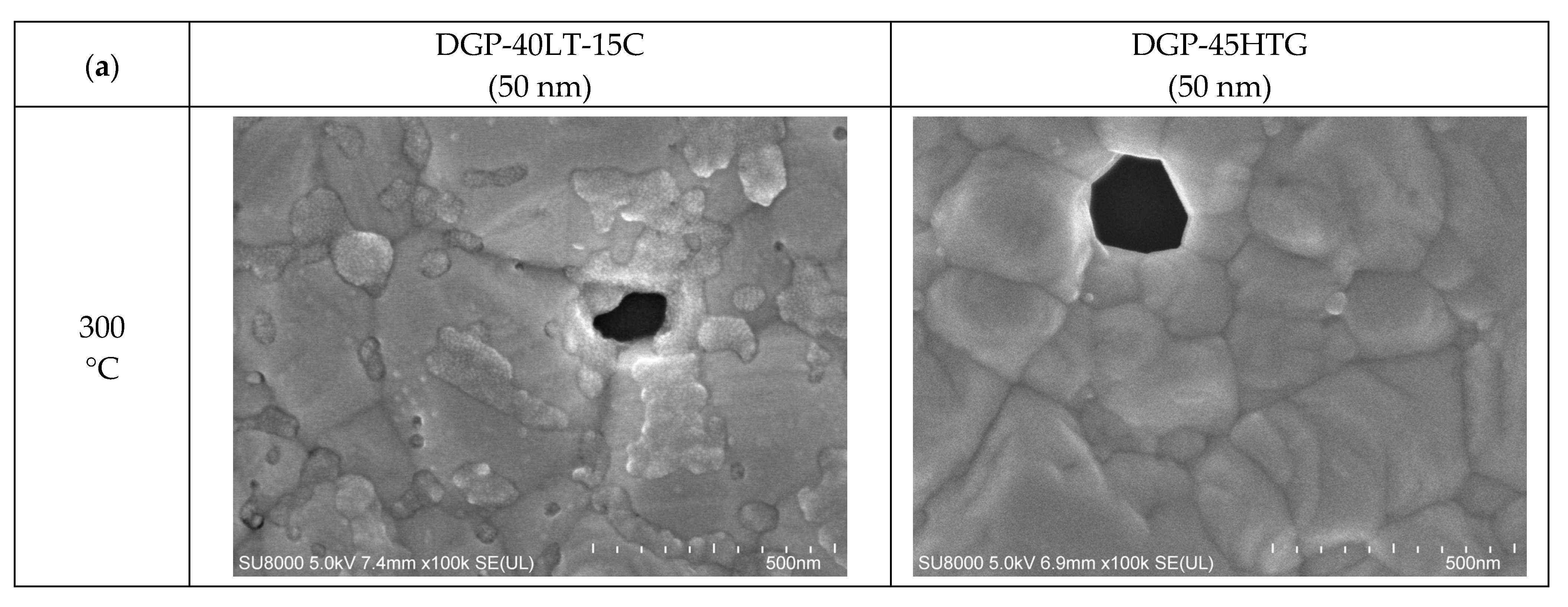
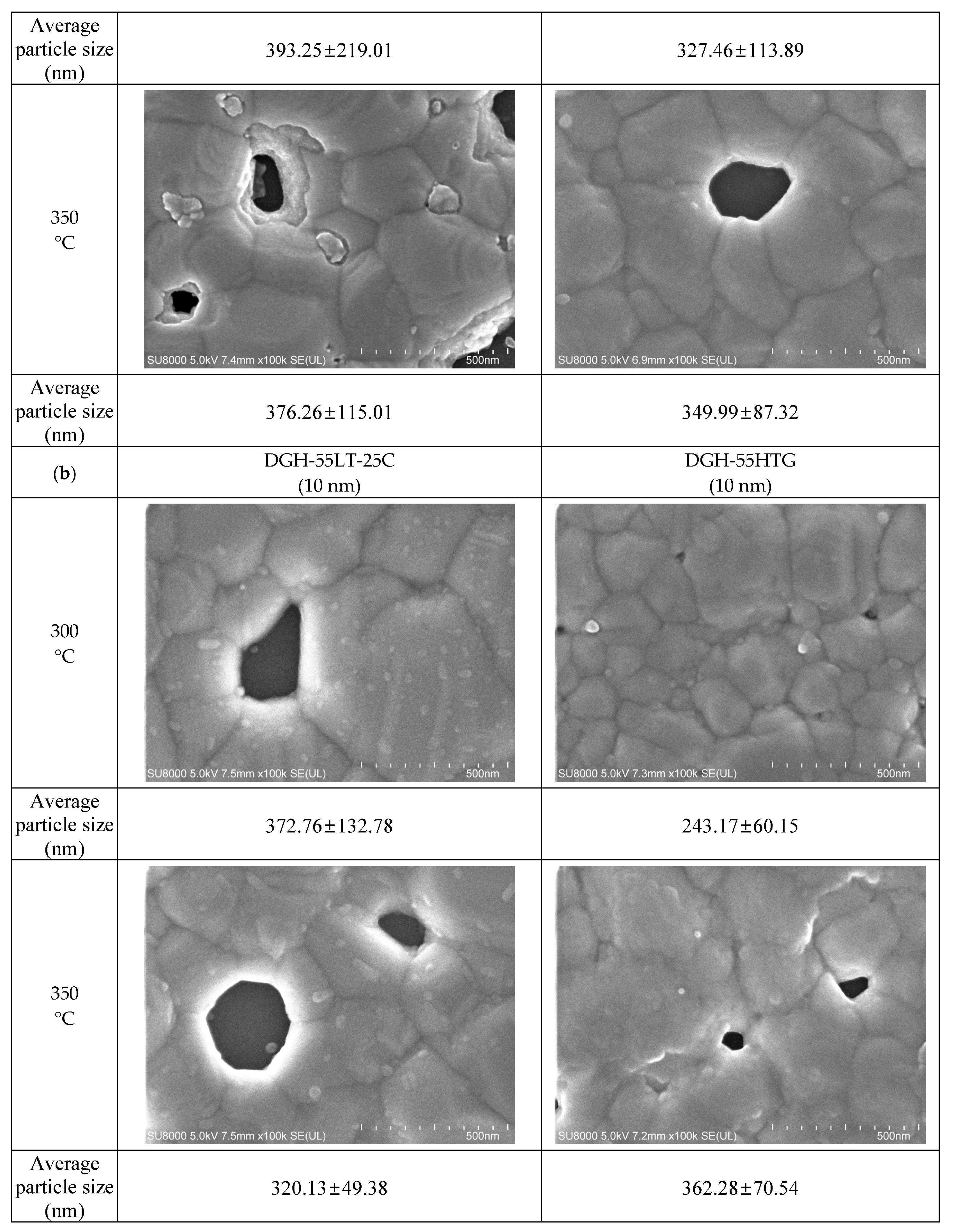
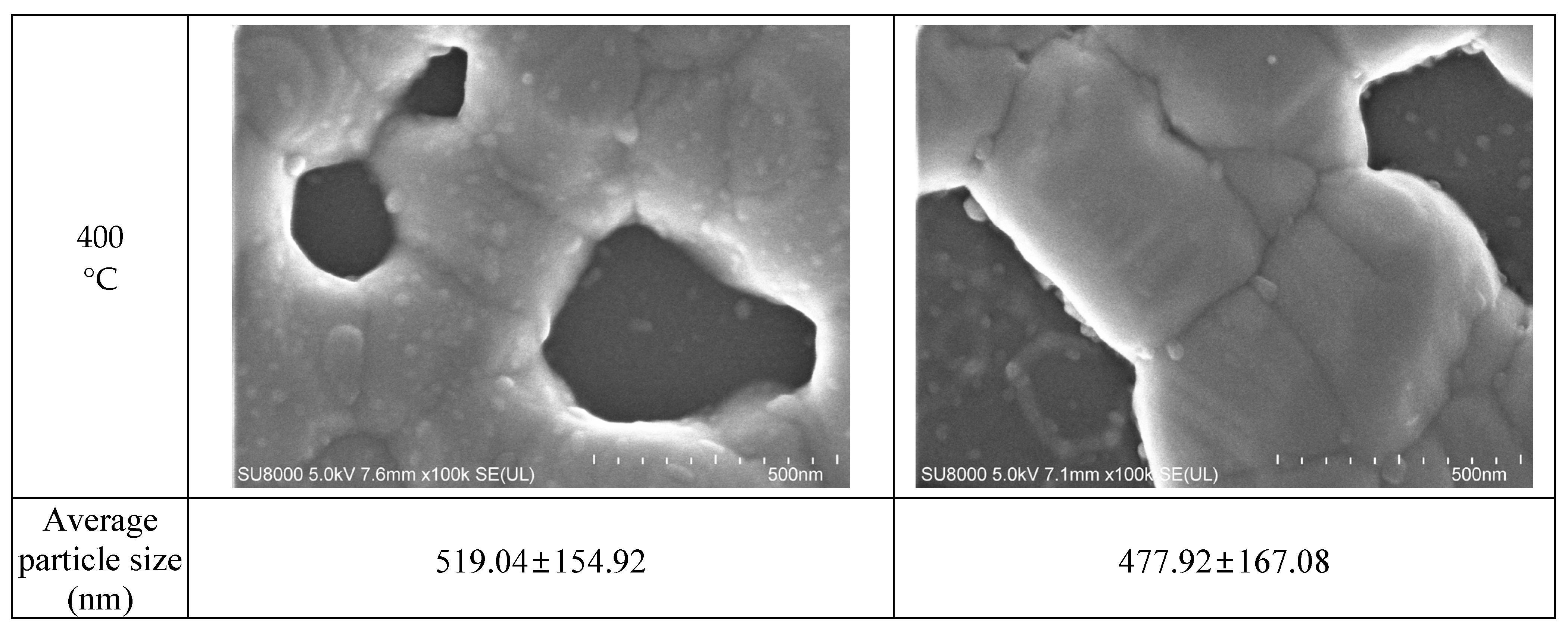
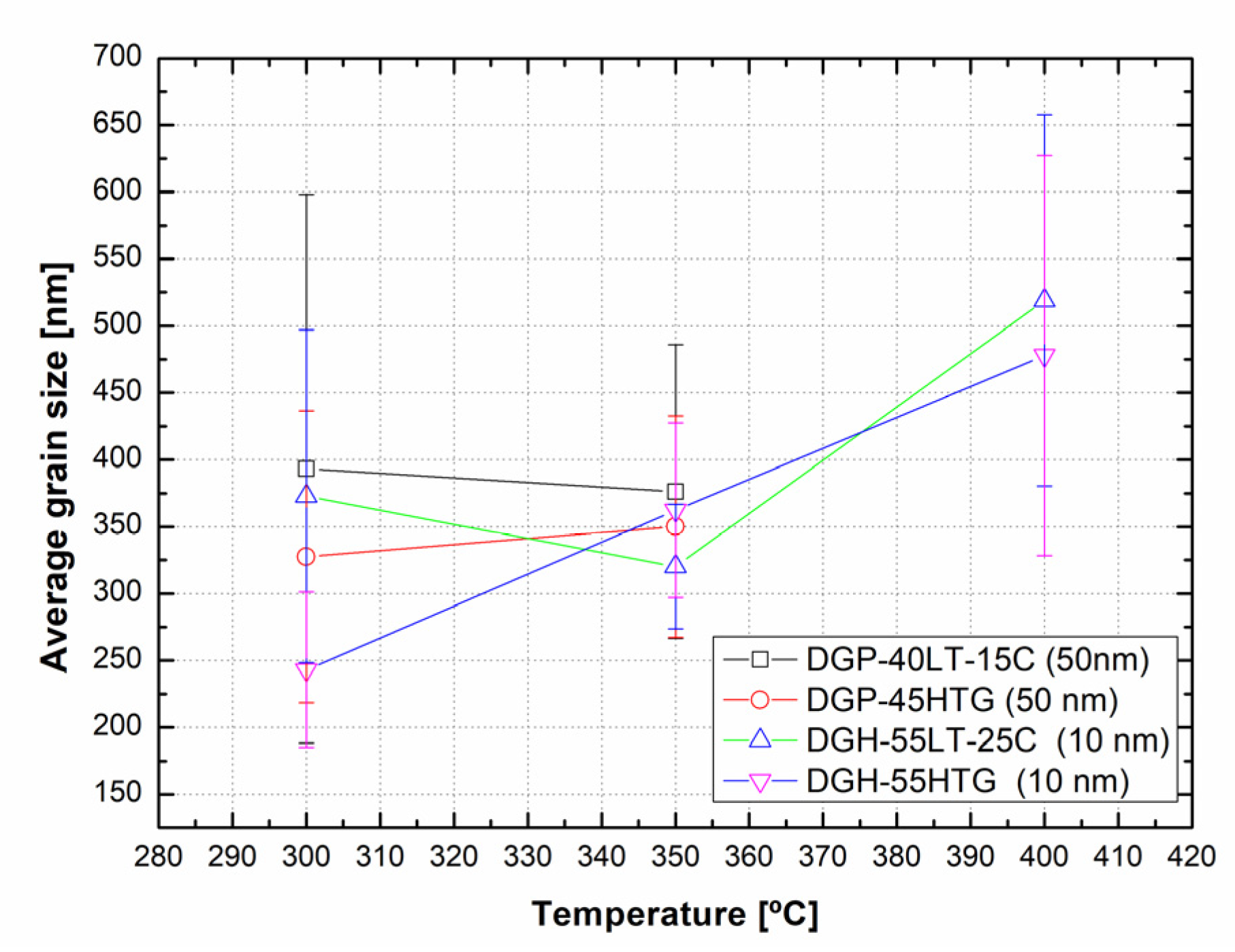
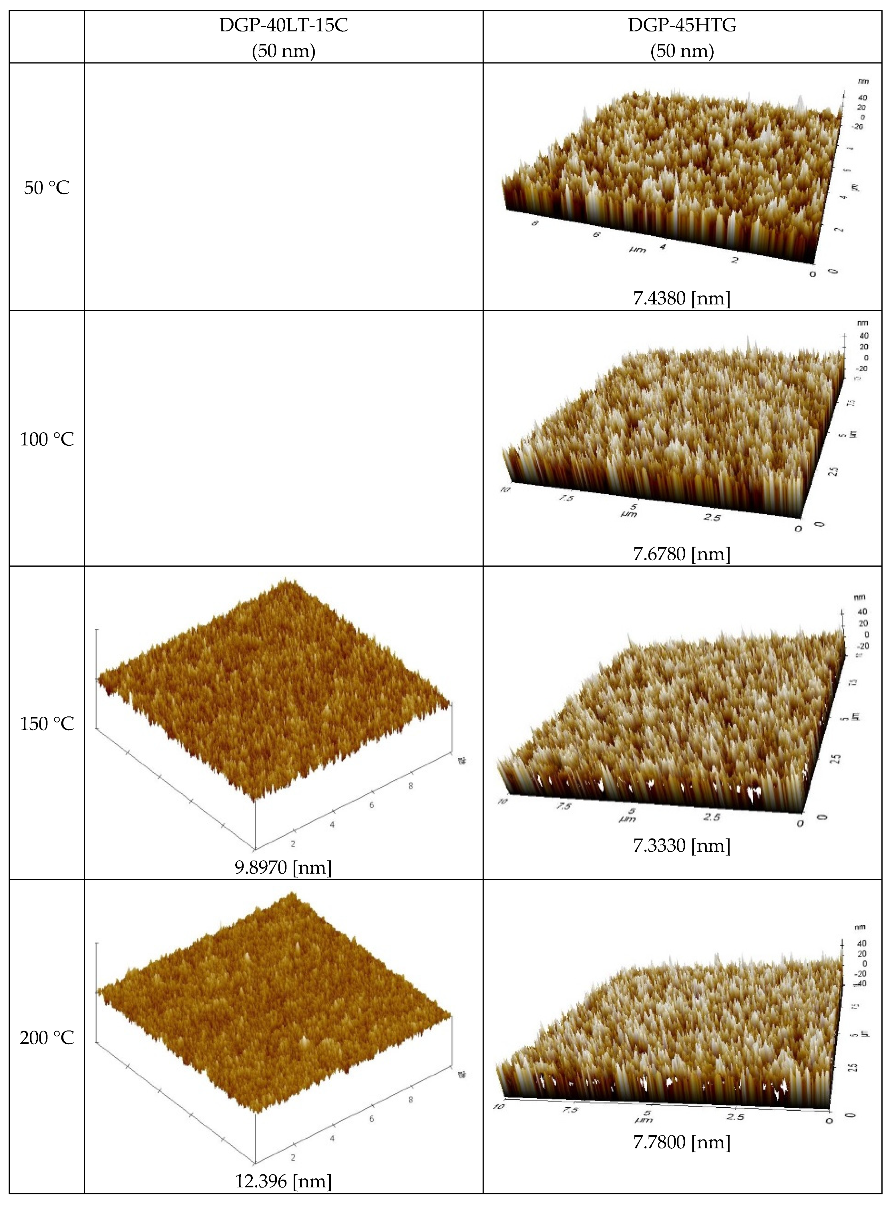
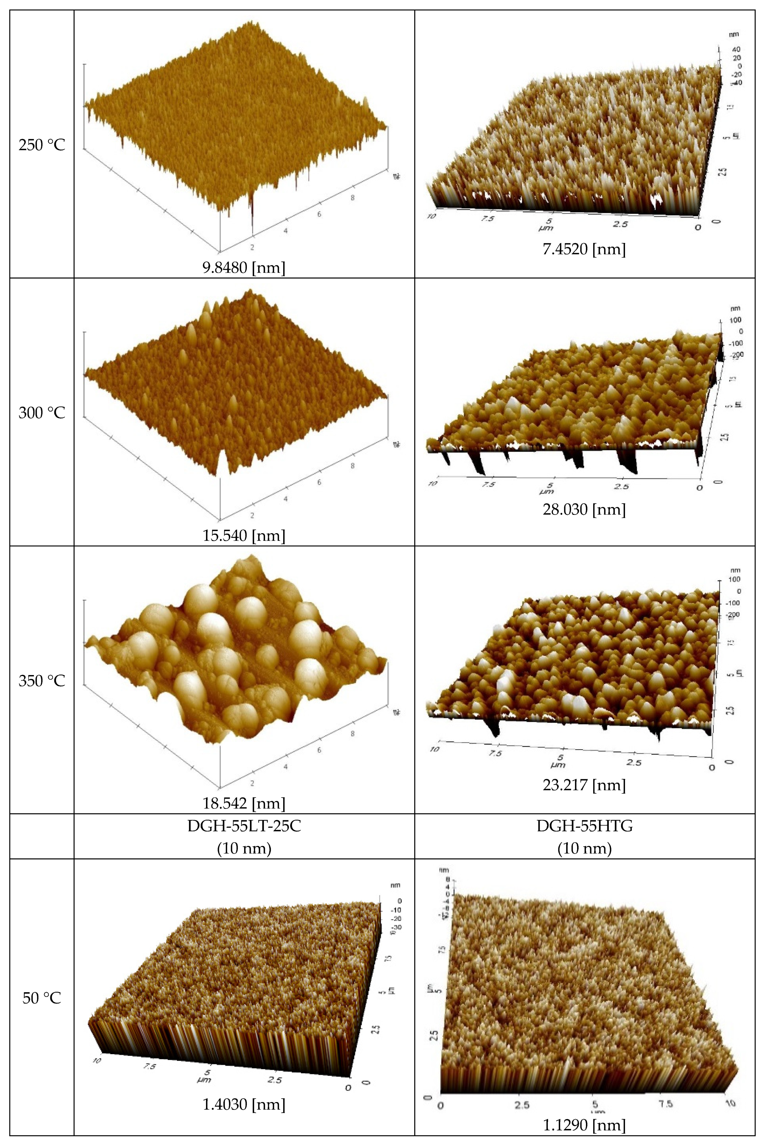
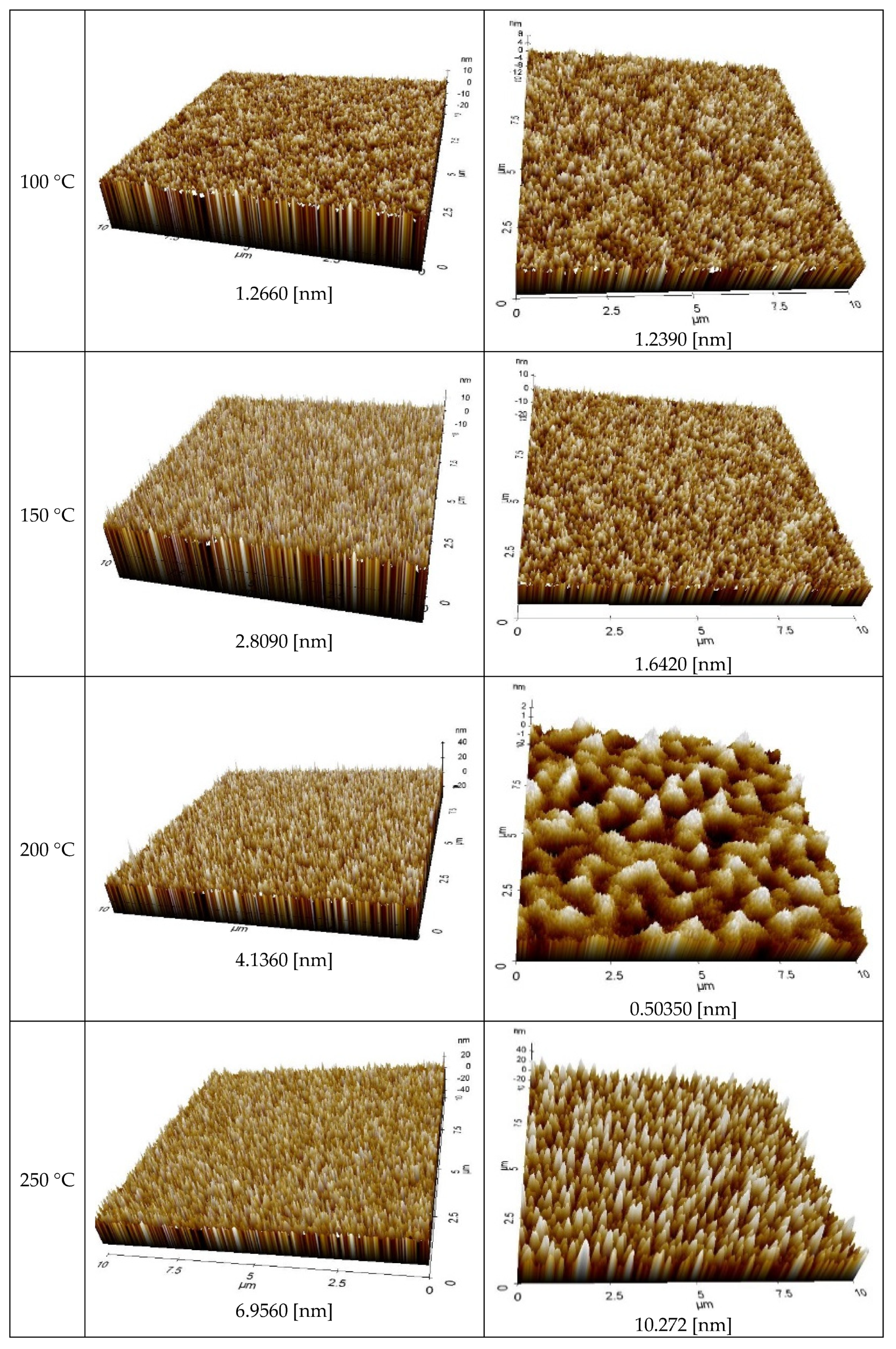
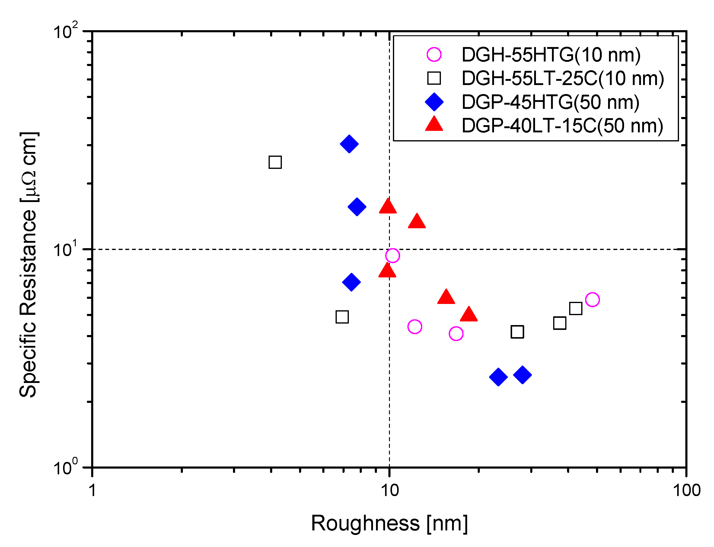
3. Results and Discussion
4. Conclusions
Author Contributions
Funding
Data Availability Statement
Conflicts of Interest
References
- Madou, M.J. Fundamentals of Microfabrication: The Science of Miniaturization; CRC Press: Boca Raton, FL, USA, 2002. [Google Scholar]
- NIPA. The Present Condition of the Global Electronic Component Industry; NIPA: Chicago, IL, USA, 2012. [Google Scholar]
- Lee, H.-H.; Chou, K.-S.; Huang, K.-C. Inkjet printing of nanosized silver colloids. Nanotechnology 2005, 16, 2436–2441. [Google Scholar] [CrossRef]
- Rance, G.A.; Marsh, D.H.; Bourne, S.J.; Reade, T.J.; Khlobystov, A.N. van der Waals Interactions between Nanotubes and Nanoparticles for Controlled Assembly of Composite Nanostructures. ACS Nano 2010, 4, 4920–4928. [Google Scholar] [CrossRef]
- You, I.K.; Koo, J.B.; Noh, Y.Y.; Yu, B.G. Technology Trend of Printed Electronics. Electron. Telecommun. Trends. 2009, 24, 41–51. [Google Scholar]
- Greer, J.R.; Street, R.A. Thermal cure effects on electrical performance of nanoparticle silver inks. Acta Mater. 2007, 55, 6345–6349. [Google Scholar] [CrossRef]
- Tan, H.W.; Saengchairat, N.; Goh, G.L.; An, J.; Chua, C.K.; Tran, T. Induction Sintering of Silver Nanoparticle Inks on Polyimide Substrates. Adv. Mater. Technol. 2020, 5, 1900897. [Google Scholar] [CrossRef]
- Liu, Q.; Xu, B.; Zhang, Y.; Wang, X.; Mei, X.; Wang, X. Picosecond laser sintering of silver paste printed by laser induced forward transfer. Opt. Laser Technol. 2021, 135, 106712. [Google Scholar] [CrossRef]
- Hussain, A.; Lee, H.L.; Moon, S.J. Sintering of silver nanoparticle structures and the pursuit of minimum resistivity. Mater. Today Commun. 2023, 34, 105159. [Google Scholar] [CrossRef]
- Kim, D.; Lee, I.; Yoo, Y.; Moon, Y.-J.; Moon, S.-J. Transient variation of a cross-sectional area of inkjet-printed silver nanoparticle ink during furnace sintering. Appl. Surf. Sci. 2014, 305, 453–458. [Google Scholar] [CrossRef]
- Dearden, A.L.; Smith, P.J.; Shin, D.; Reis, N.; Derby, B.; O’Brien, P. A low curing temperature silver ink for use in ink-jet printing and subsequent production of conductive tracks. Macromol. Rapid Commun. 2005, 26, 315–318. [Google Scholar] [CrossRef]
- Fuller, S.B.; Wilhelm, E.J.; Jacobson, J.M. Ink-jet printed nanoparticle microelectromechanical systems. J. Microelectromech. Syst. 2002, 11, 54–60. [Google Scholar] [CrossRef]
- Kim, D.; Moon, J. Highly conductive ink jet printed films of nanosilver particles for printable electronics. Electrochem. Solid-state Lett. 2005, 8, J30–J33. [Google Scholar] [CrossRef]
- Zacharatos, F.; Theodorakos, I.; Karvounis, P.; Tuohy, S.; Braz, N.; Melamed, S.; Kabla, A.; De la Vega, F.; Andritsos, K.; Hatziapostolou, A.; et al. Selective laser sintering of laser printed Ag nanoparticle micropatterns at high repetition rates. Materials 2018, 11, 2142. [Google Scholar] [CrossRef] [PubMed]
- Allen, M.L.; Aronniemi, M.; Mattila, T.; Alastalo, A.; Ojanperä, K.; Suhonen, M.; Seppä, H. Electrical sintering of nanoparticle structures. Nanotechnology 2008, 19, 175201. [Google Scholar] [CrossRef] [PubMed]
- Reinhold, I.; Hendriks, C.E.; Eckardt, R.; Kranenburg, J.M.; Perelaer, J.; Baumann, R.R.; Schubert, U.S. Argon plasma sintering of inkjet printed silver tracks on polymer substrates. J. Mater. Chem. 2009, 19, 3384–3388. [Google Scholar] [CrossRef]
- Perelaer, J.; Jani, R.; Grouchko, M.; Kamyshny, A.; Magdassi, S.; Schubert, U.S. Plasma and Microwave Flash Sintering of a Tailored Silver Nanoparticle Ink, Yielding 60% Bulk Conductivity on Cost-Effective Polymer Foils. Adv. Mater. 2012, 24, 3993–3998. [Google Scholar] [CrossRef] [PubMed]
- Perelaer, J.; De Gans, B.-J.; Schubert, U.S. Ink-jet Printing and Microwave Sintering of Conductive Silver Tracks. Adv. Mater. 2006, 18, 2101–2104. [Google Scholar] [CrossRef]
- Perelaer, J.; Klokkenburg, M.; Hendriks, C.E.; Schubert, U.S. Microwave Flash Sintering of Inkjet-Printed Silver Tracks on Polymer Substrates. Adv. Mater. 2009, 21, 4830–4834. [Google Scholar] [CrossRef]
- Lee, D.-G.; Kim, D.K.; Moon, Y.-J.; Moon, S.-J. Effect of temperature on electrical conductance of inkjet-printed silver nanoparticle ink during continuous wave laser sintering. Thin Solid Films 2013, 546, 443–447. [Google Scholar] [CrossRef]
- Ryu, K.; Moon, Y.-J.; Park, K.; Hwang, J.-Y.; Moon, S.-J. Electrical Property and Surface Morphology of Silver Nanoparticles After Thermal Sintering. J. Electron. Mater. 2016, 45, 312–321. [Google Scholar] [CrossRef]
- Paeng, D.; Lee, D.; Grigoropoulos, C.P. Characteristic time scales of coalescence of silver nanocomposite and nanoparticle films induced by continuous wave laser irradiation. Appl. Phys. Lett. 2014, 105, 073110. [Google Scholar] [CrossRef]
- Hussain, A.; Lee, H.-L.; Moon, Y.-J.; Hwang, J.Y.; Moon, S.-J. Effect of pulse overlapping on temperature field and physical characteristics in pulsed laser sintering of inkjet-printed silver nanoparticles. Int. J. Heat Mass Transf. 2023, 202, 123678. [Google Scholar] [CrossRef]
- Lee, I.; Hussain, A.; Lee, H.-L.; Moon, Y.-J.; Hwang, J.-Y.; Moon, S.-J. The effect of current supply duration during stepwise electrical sintering of silver nanoparticles. Metals 2021, 11, 1878. [Google Scholar] [CrossRef]
- Rahimian, M.; Ehsani, N.; Parvin, N.; Baharvandi, H.R. The effect of particle size, sintering temperature and sintering time on the properties of Al–Al2O3 composites, made by powder metallurgy. J. Mater. Process. Technol. 2009, 209, 5387–5393. [Google Scholar] [CrossRef]
- Kim, C.; Nogi, M.; Suganuma, K. Electrical conductivity enhancement in inkjet-printed narrow lines through gradual heating. J. Micromechanics Microengineering 2012, 22, 035016. [Google Scholar] [CrossRef]
- Asoro, M.; Kovar, D.; Damiano, J.; Ferreira, P. Scale Effects on the Melting Behavior of Silver Nanoparticles. Microsc. Microanal. 2010, 16, 1802–1803. [Google Scholar] [CrossRef]
- Luo, W.; Hu, W.; Xiao, S. Size effect on the thermodynamic properties of silver nanoparticles. J. Phys. Chem. C 2008, 112, 2359–2369. [Google Scholar] [CrossRef]
- Buffat, P.; Borel, J.-P. Size effect on the melting temperature of gold particles. Phys. Rev. A 1976, 13, 2287–2298. [Google Scholar] [CrossRef]
- Yang, C.C.; Li, S. Investigation of cohesive energy effects on size-dependent physical and chemical properties of nanocrystals. Phys. Rev. B Condens. Matter Mater. Phys. 2007, 75, 165413. [Google Scholar] [CrossRef]
- Jiang, Q.; Zhang, S.; Zhao, M. Size-dependent melting point of noble metals. Mater. Chem. Phys. 2003, 82, 225–227. [Google Scholar] [CrossRef]
- Liang, T.; Zhou, D.; Wu, Z.; Shi, P. Size-dependent melting modes and behaviors of Ag nanoparticles: A molecular dynamics study. Nanotechnology 2017, 28, 485704. [Google Scholar] [CrossRef]
- Bochnia, J. A Study of the mechanical properties of Naturally Aged Photopolymers Printed Using the PJM Technology. Materials 2023, 16, 400. [Google Scholar] [CrossRef]
- Baroutaji, A.; Arjunan, A.; Beal, J.; Robinson, J.; Coroado, J. The influence of atmospheric Oxygen Content on the Mechanical Properties of Selectively Laser Melted AlSi10Mg TPMS-Based Lattice. Materials 2023, 16, 430. [Google Scholar] [CrossRef] [PubMed]
- Formisano, A.; Boccarusso, L.; Durante, M. Optimization of single-point incremental forming of polymer sheets through FEM. Materials 2023, 16, 451. [Google Scholar] [CrossRef] [PubMed]
- Wei, B.; Yu, C.; Bai, Y.; Liu, L.; He, J. Preparation Optimization of CFRP and EPDM Composite by the Co-Curing Method. Materials 2023, 16, 503. [Google Scholar] [CrossRef]
- Sobolev, A.; Musin, A.; Whyman, G.; Borodianskiy, K.; Krichevski, O.; Kalashnikov, A.; Zinigrad, M. Stabilization of cubic phase in scandium-doped zirconia nanocrystals synthesized with sol-gel method. J. Am. Ceram. Soc. 2019, 102, 3236–3243. [Google Scholar] [CrossRef]
- Yamashita, M. Geometrical Correction Factor for Resistivity of Semiconductors by the Square Four-Point Probe Method. Jpn. J. Appl. Phys. 1986, 25, 563–567. [Google Scholar] [CrossRef]
- Nguyen, L.-N.; Pradhan, S.K.; Yen, C.-N.; Lin, M.-C.; Chen, C.-H.; Wu, C.-S.; Chang-Liao, K.-S.; Lin, M.-T.; Chen, C.-D. High performance phototransistors based on single crystalline perylene-tetracarboxylic-dianhydride nanoparticle. Appl. Phys. Lett. 2013, 103, 183301. [Google Scholar] [CrossRef]
- Ingham, B.; Lim, T.H.; Dotzler, C.J.; Henning, A.; Toney, M.F.; Tilley, R.D. How Nanoparticles Coalesce: An in Situ Study of Au Nanoparticle Aggregation and Grain Growth. Chem. Mater. 2011, 23, 3312–3317. [Google Scholar] [CrossRef]
- Kang, S.-J.L. Sintering: Densification, Grain Growth and Microstructure; Elsevier: Amsterdam, The Netherlands, 2004. [Google Scholar]
- Voorhees, P.W. The theory of Ostwald ripening. J. Stat. Phys. 1985, 38, 231–252. [Google Scholar] [CrossRef]


| DGP-40LT-15C (50 nm) | DGP-45HTG (50 nm) | DGH-55HTG (10 nm) | DGH-55LT-25C (10 nm) | |
|---|---|---|---|---|
| Ag content (wt%) | 31 | 32 | 56 | 58 |
| Particle size (nm) | ~50 | ~50 | ~10 | ~10 |
| Viscosity (cPs) | 10~17 | 18.2 | 9.75 | 8.0 |
| Surface tension (mN·m−1) | 36 | 37.4 | 29.2 | 29.2 |
| Solvent | TGME | TGME | Tetradecane | Tetradecane |
| Curing temp. (°C) | 150 °C | 400 °C | 400 °C | 250 °C |
| Specific resistance (μΩ·cm) | 11~12 | 2~3 | 2.0~2.5 | 2.4~3.0 |
| Substrate | Eagle XG glass | Eagle XG glass | Eagle XG glass | Eagle XG glass |
Disclaimer/Publisher’s Note: The statements, opinions and data contained in all publications are solely those of the individual author(s) and contributor(s) and not of MDPI and/or the editor(s). MDPI and/or the editor(s) disclaim responsibility for any injury to people or property resulting from any ideas, methods, instructions or products referred to in the content. |
© 2024 by the authors. Licensee MDPI, Basel, Switzerland. This article is an open access article distributed under the terms and conditions of the Creative Commons Attribution (CC BY) license (https://creativecommons.org/licenses/by/4.0/).
Share and Cite
Park, H.-J.; Ryu, K.; Lee, H.-L.; Moon, Y.-J.; Hwang, J.Y.; Moon, S.J. Physical Characteristics of Sintered Silver Nanoparticle Inks with Different Sizes during Furnace Sintering. Materials 2024, 17, 978. https://doi.org/10.3390/ma17050978
Park H-J, Ryu K, Lee H-L, Moon Y-J, Hwang JY, Moon SJ. Physical Characteristics of Sintered Silver Nanoparticle Inks with Different Sizes during Furnace Sintering. Materials. 2024; 17(5):978. https://doi.org/10.3390/ma17050978
Chicago/Turabian StylePark, Hyeong-Jin, Kyongtae Ryu, Hee-Lak Lee, Yoon-Jae Moon, Jun Young Hwang, and Seung Jae Moon. 2024. "Physical Characteristics of Sintered Silver Nanoparticle Inks with Different Sizes during Furnace Sintering" Materials 17, no. 5: 978. https://doi.org/10.3390/ma17050978
APA StylePark, H.-J., Ryu, K., Lee, H.-L., Moon, Y.-J., Hwang, J. Y., & Moon, S. J. (2024). Physical Characteristics of Sintered Silver Nanoparticle Inks with Different Sizes during Furnace Sintering. Materials, 17(5), 978. https://doi.org/10.3390/ma17050978