Abstract
Pyroelectric materials are naturally electrically polarized and exhibits a built-in spontaneous polarization in their unit cell structure even in the absence of any externally applied electric field. These materials are regarded as one of the ideal detector elements for infrared applications because they have a fast response time and uniform sensitivity at room temperature across all wavelengths. Crystals of the perovskite lead titanate (PbTi) family show pyroelectric characteristics and undergo structural phase transitions. They have a high Curie temperature (the temperature at which the material changes from the ferroelectric (polar) to the paraelectric (nonpolar) phase), high pyroelectric coefficient, high spontaneous polarization, low dielectric constant, and constitute important component materials not only useful for infrared detection, but also with vast applications in electronic, optic, and MEMS devices. However, the preparation of large perfect and pure single crystals PbTi is challenging. Additionally, difficulties arise in the application of such bulk crystals in terms of connection to processing circuits, large size, and high voltages required for their operation. In this part of the review paper, we explain the electrical behavior and characterization techniques commonly utilized to unravel the pyroelectric properties of lead titanate and its derivatives. Further, it explains how the material preparation techniques affect the electrical characteristics of resulting thin films. It also provides an in-depth discussion of the measurement of pyroelectric coefficients using different techniques.
1. Introduction
The electrical characteristics and characterization methods of magnetron-sputtered lead titanate thin films play a crucial role in understanding and optimizing their performance for pyroelectric applications. In this second part of the review article, we focus on providing a comprehensive insight into the advances made in the electrical characterization of these materials. A key aspect of this exploration is the systematic study of the conduction mechanism within lead titanate thin films. It is essential to explore the conduction mechanism as it can provide information about phenomena such as contact effects, the physical nature of the interface, and the bulk space charges that often dominate the transport mechanisms in these materials. By delving into the conduction mechanisms, researchers can gain invaluable information about the intricate interplay of charges and the material’s electrical properties. Understanding the conduction mechanisms becomes particularly crucial when addressing device-reliability issues. Imprint, for instance, refers to the preference of a ferroelectric (FE) capacitor for one polarization state over the other. Investigating the conduction mechanisms aids in deciphering the factors influencing imprint and finding ways to mitigate its effects, thereby enhancing the stability and reliability of devices. Fatigue is another important reliability concern, involving the loss of polarization due to bipolar cycling of the capacitor. By studying the conduction mechanisms, researchers can identify the underlying causes of fatigue and develop strategies to improve the endurance of lead titanate thin films in practical applications. Polarization relaxation, characterized by the momentary lag in the dielectric constant of a material, is also a significant aspect addressed in the electrical characterization. This phenomenon is typically caused by the delay in molecular polarization concerning a changing electric field in a dielectric medium. Understanding the conduction mechanisms aids in elucidating the factors contributing to polarization relaxation, enabling researchers to design materials with improved response times. Resistance degradation and breakdown are additional challenges that demand a thorough exploration of the electrical characteristics. It is essential to identify the mechanisms leading to resistance degradation and breakdown to ensure the longevity and robustness of devices based on magnetron-sputtered lead titanate thin films. In conclusion, the systematic study of the conduction mechanisms in lead titanate thin films offers crucial insights into various electrical phenomena and device-reliability issues. This knowledge is instrumental in advancing the understanding and optimization of these materials for pyroelectric applications, ultimately paving the way for enhanced performance and reliability in practical devices [1].
2. Measurement of the Electrical Characteristics
Methods developed for the electrical characterization of FE materials such as current-voltage, I(V), current-time, I(t), capacitance-voltage dielectric constant- electric field , and polarization-electric field are also compatible with the characterization of the pyroelectrics. However, for pyroelectric materials, the measurement of the pyroelectric coefficient, is also extremely important. In this part, we discuss the abovementioned development and measurement methods and identify the strongest stress on thin-film pyroelectric materials. In this section, we delve further into the specific electrical characterization methods and processes relevant to thin film pyroelectric materials, as outlined in the following. The first point is the measurement of hysteresis. Hysteresis curves are essential for understanding the ferroelectric and pyroelectric behavior of materials. By applying an electric field and measuring the polarization response, researchers can characterize the hysteresis loop, providing insights into the switching dynamics and polarization properties of thin-film pyroelectric materials. Second, dielectric permittivity measurements involve determining the ability of a material to store electrical energy in an electric field. This is crucial for understanding the energy storage capabilities of thin-film pyroelectric materials, influencing their performance in various applications. Third, the measurement of capacitance-voltage characteristics provides information about the capacitive properties and response to varying voltages since capacitance-voltage characteristics are pivotal for understanding the charge storage and transport mechanisms in thin-film pyroelectric materials. The fourth point is that the measurement of leakage current characteristics in lead titanate (PT)-based thin films helps identify potential issues such as defects or breakdowns that could affect device performance, where it is critical to understand leakage currents to assess the integrity and reliability of pyroelectric devices. Fifth, fatigue measurements involve studying the degradation of polarization over repeated cycles. Assessing fatigue in PT-based materials is essential for predicting the lifespan and durability of pyroelectric devices. Techniques such as pulse testing or continuous cycling are employed for fatigue evaluation. Sixth, poling is a process where an electric field is applied to align the polar domains in a ferroelectric or pyroelectric material. For thin-film pyroelectric materials, optimizing the poling process is crucial for enhancing their pyroelectric performance and ensuring a stable polarization state. Then, pyroelectric measurements involve assessing the ability of a material to generate polarization in response to temperature changes. These measurements, often involving the pyroelectric coefficient (p), are fundamental for characterizing the pyroelectric properties of thin-film materials. Lastly, understanding the interplay between the processing methods and resulting electrical properties is crucial for optimizing thin-film pyroelectric materials. Factors such as deposition techniques, annealing processes, and film thickness can significantly influence the electrical characteristics of the material.
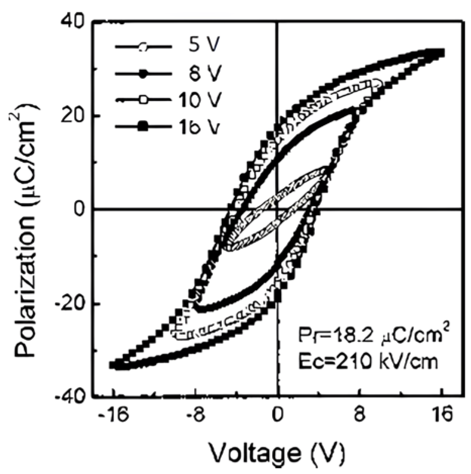
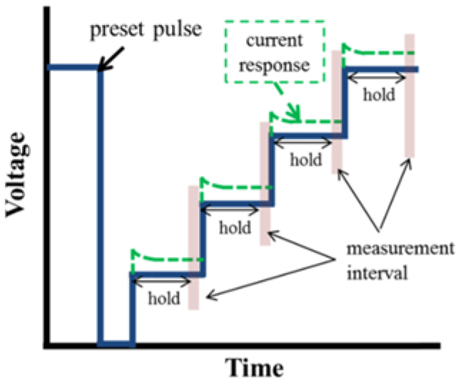
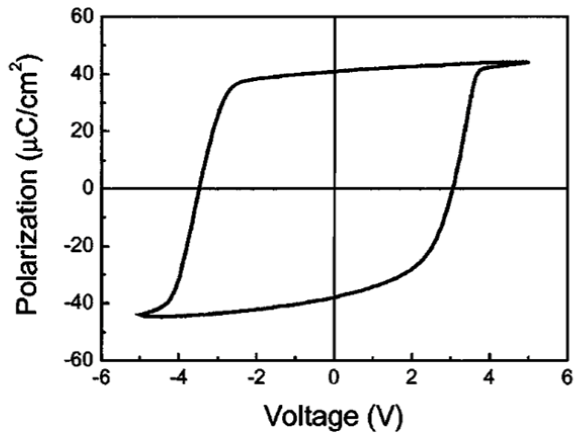
2.1. Measurement of the Hysteresis Curves
A P(E) loop is a plot of the charge per unit area or polarization (P) developed because of a field applied to that device (E) at a given frequency. Most testing methods of FE capacitors utilize either charge or current integration techniques for measuring hysteresis loops (see Appendix A.1). Hysteresis loops in the context of lead titanate films play a crucial role in understanding and characterizing the electrical behavior of these materials. Hysteresis, in general, refers to the phenomenon where the response of a system lags behind and depends on its history. In the case of lead titanate films, hysteresis loops are often observed in the polarization-electric field curve. These loops are indicative of the ferroelectric nature of lead titanate films. Ferroelectric materials, such as lead titanate, exhibit spontaneous polarization that can be switched by an external electric field. The hysteresis loop represents the relationship between the polarization and the applied electric field during both the polarization and depolarization processes. The significance of hysteresis loops lies in their ability to provide insights into the ferroelectric properties of lead titanate films. The loop’s shape and size can reveal information about the coercive field (the electric field required to switch the polarization) and the remanent polarization (the polarization retained when the external field is removed). These parameters are crucial in understanding the switching behavior and stability of lead titanate films. In practical applications, lead titanate films are used in various devices, including ferroelectric random access memory (FeRAM), sensors, actuators, and transducers. The ability to control and manipulate polarization in lead titanate films, as indicated by hysteresis loops, is exploited in these applications. For example, in FeRAM, the hysteresis loop characteristics help store and retrieve information based on the polarization states, providing a non-volatile memory solution. Hysteresis loops in pyroelectric materials are typically measured using a ferroelectric tester or a precision analyzer. The material is subjected to an oscillating electric field, and the resulting polarization is recorded as a function of the applied field. The hysteresis loop provides information about the ferroelectric and pyroelectric properties of the material. Understanding the coercive field, remanent polarization, and switching behavior is crucial for optimizing the material’s performance in pyroelectric applications. The hysteresis loop provides insight into the switching behavior, essential for the design of reliable infrared sensors.
Pintilie et al. [2] measured the hysteresis loop at 1 kHz using a TF 2000 analyzer in dynamic mode (aixACCT Systems GmbH, Aachen, Germany) for the epitaxial Pb()(PZT) layers with both top and bottom electrodes made of SrRu(SRO).
As shown in Figure 1, typically, a remnant polarization of about 40 μC/ and a coercive field of about 150 kV/cm was achieved [2]. The shape of the hysteresis loop is nearly rectangular and very close to an ideal loop. Yet, the reversal is not symmetric with voltage polarity, which suggests that the two FE interfaces with the electrodes are not equivalent, as discussed later.
Figure 1.
A typical hysteresis loop acquired on an epitaxial SRO/PZT (20/80)/SRO layer structure at 1 kHz [2]. Reproduced from [2], Figure 1, Figure 2, Figure 3 and Figure 4, with the permission of AIP Publishing. https://doi.org/10.1063/1.1926403.
Tang, et al. [3] prepared 200 nm thick, highly (111)-oriented () Ti (PCT) thin films on Pt/Ti/Si/Si substrates using a sol–gel process. Their capacitor structure consisted of top (0.2-mm diameter, Ohmic) Au/PCT/bottom (Schottky) Pt on Ti/Si/Si (100) substrate. Figure 2 shows the typical P(E) hysteresis loops at an applied field of 800 kV/cm with remnant polarization () and coercive electric field () values of 18.2 m C/ and 210 kV/cm, respectively [3].
Figure 2 shows that the P(E) hysteresis loop is asymmetric, with an imprint voltage . The voltage shift indicates the presence of a trap distribution near film-substrate interface [4], and its magnitude is affected by parameters such as the top and bottom electrodes’ work function difference, the magnitude of polarization, and/or the contribution of defect-dipole complexes. The polarization establishes a potential well that attracts the charge carriers to the interfacial defect sites where they are trapped. Remnant polarization and coercive electric field for several processes are compared in Table 1.
Table 1.
Remnant polarization and coercive electric field for several processes.
Asymmetrical contacts to FE films lead to the built-in electric fields and imprint the FE hysteresis loop toward one bias [7]. Simulation has shown that unequal Schottky barriers at the film/electrode interface are the main source of imprint [8]. Symmetrical electrodes can also give rise to the imprint due to the presence of a fabrication defect-induced passive layer within the metal/FE/metal capacitor [9]. Imprint can be beneficial since it allows the observation of high field properties even at low or zero applied fields. In pyroelectric applications, beneficial pyroelectric coefficients increase, and detrimental dielectric loss decreases at higher fields [10]. It is valuable to observe these properties at lower fields.
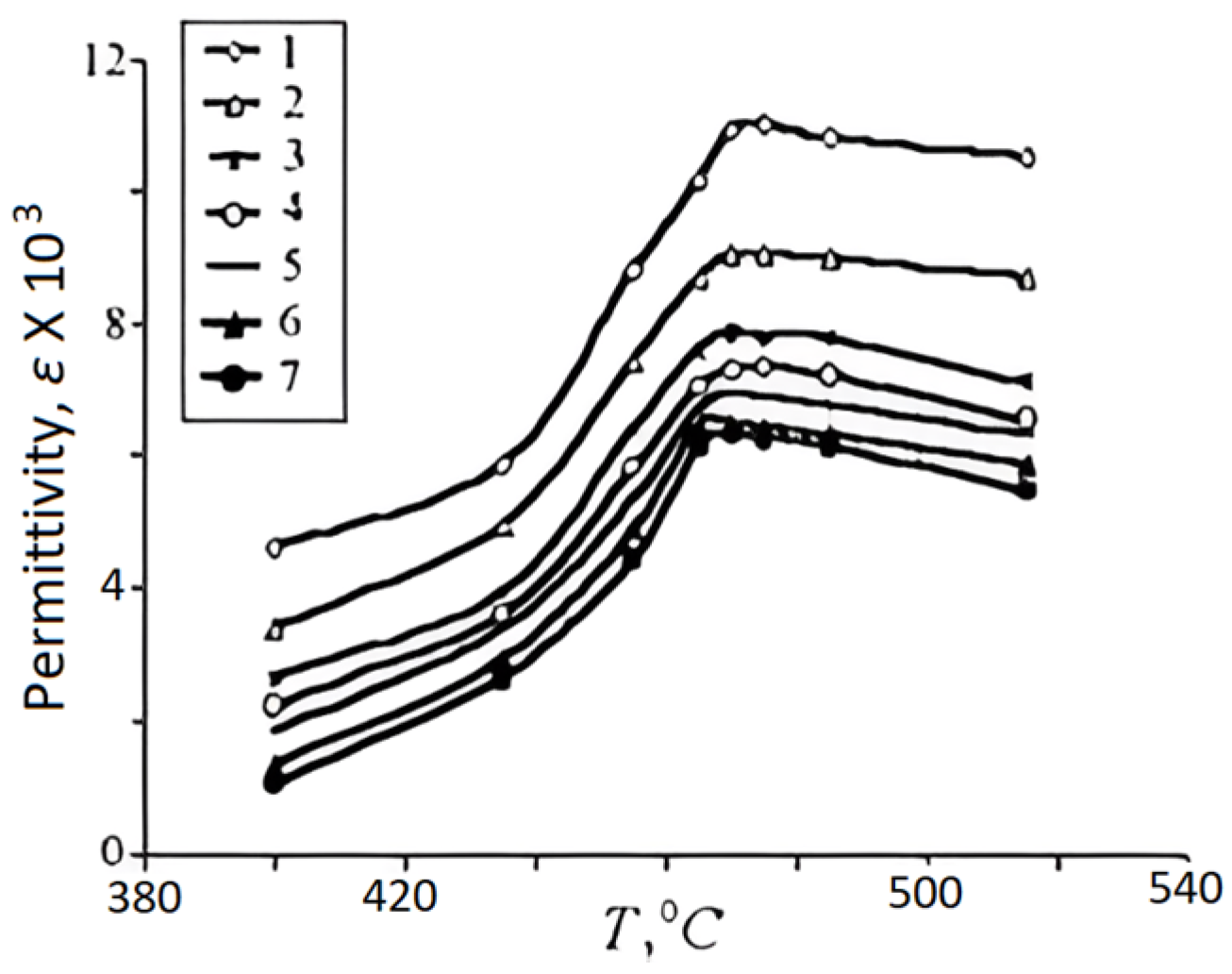
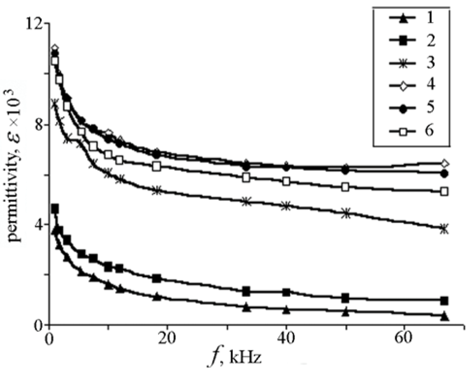
2.2. Measurement of the Dielectric Permittivity
The relative permittivity () of a dielectric (dielectric constant) indicates to what extent a finite volume of a dielectric is polarized when it is biased under an electric field. Dielectric permittivity is often measured using impedance analyzers or LCR meters. The sample is subjected to an alternating electric field, and the response in terms of capacitance and phase shift is analyzed. Dielectric permittivity is indicative of the material’s ability to store electrical energy. In pyroelectric materials, the permittivity may change with temperature, affecting the material’s overall pyroelectric response. Understanding dielectric permittivity aids in designing efficient pyroelectric energy harvesting devices that can convert temperature variations into electrical energy. Sidorkin et al. [11] prepared lead titanate films on using layer by layer magnetron sputter deposition of Ti and Pb in an argon environment, without interruption to atmosphere, in a chamber evacuated to a pressure of Pa, followed by annealing in at 700 °C for one hour. Under these conditions, a in the deposited films provided optimal PT stoichiometry and crystallinity. The frequency dependence of , for (around of the phase transition temperature) and the temperature dependence of for are shown in Figure 3 and Figure 4, respectively [11]. Measurements were carried out under an applied voltage of .
Curie temperature (Tc) is the temperature at which any in Figure 3 reaches its maximum and marks the borderline between (orthorhombic) ferro- and (cubic) para-electric phases. In other words, the Curie temperature is defined as the temperature when the phase of a material changes because of the application of an electric field. Like the bulk samples, Figure 4 shows a relaxation character of dispersion: At any temperature, is reduced as is increased, and at high frequencies, it assumes a relatively constant value. This behavior stems from dipole inertia: Various dipoles lag behind the electric field. At low frequencies, all the dipoles contribute to the value of the dielectric constant. As the frequency is increased, those dipoles with larger relaxation time constants cease to respond and hence, the dielectric constant decreases. The delay in response leads to a loss and decline in the dielectric constant.
The dielectric constant of thin film ferroelectric materials is smaller than that of their bulk counterparts and generally decreases as the film thickness is reduced [12]. It is measured via the capacitance of parallel plate-type capacitors at the low-frequency end and is interpreted in terms of an interfacial layer with the low dielectric constant in series with the bulk dielectric. Such a rationale conforms with theoretical polarization models since the loss of dipole-dipole interactions at the film interface results in the reduction of the dielectric constant. A second source contributing to the reduction of the measured capacitance from the value expected for an ideal parallel plate capacitor is associated with electric field penetration into the metal electrodes [13,14]. However, the dielectric properties of the thin films depend on their microstructure, and it is challenging to separate the influence of thickness-dependent variations in the microstructure on the dielectric constant from intrinsic thickness variations of the dielectric constant. Studies on the dielectric properties of thin polycrystalline (PZT) films conform with the general thickness dependence trend [15,16]. For epitaxial films, Fujisawa et al. [17] report that the variation of the dielectric constant with thickness is smaller compared to that of polycrystalline PZT films. Pintilie et al. [18] found that the intrinsic dielectric constant is close to the measured value in the fully depleted thin films and attributed the decrease in the dielectric constant with decreasing film thickness to the leaky bulk region of the film.
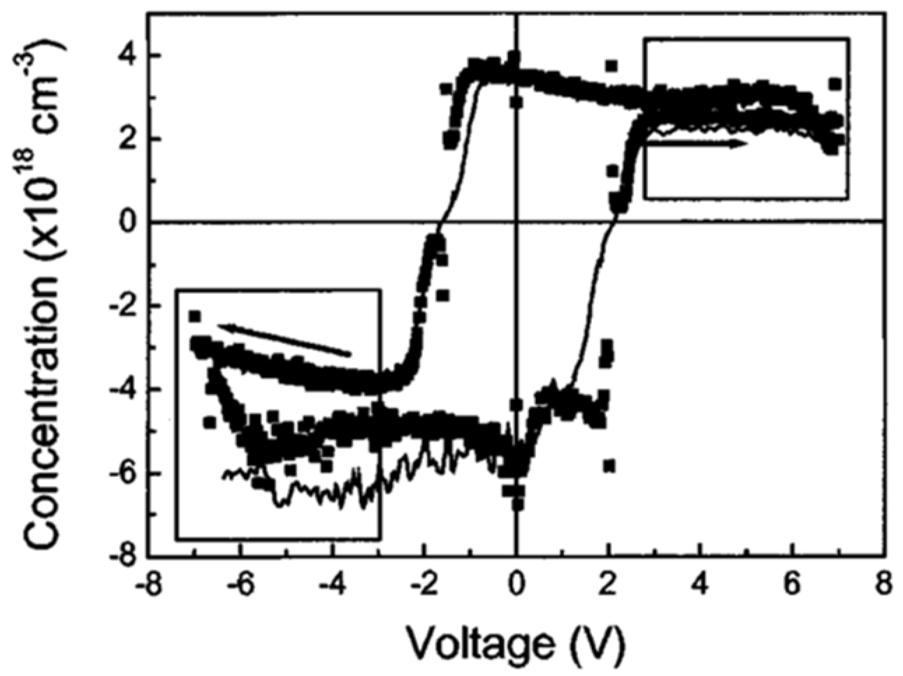
2.3. Measurement of Capacitance-Voltage Characteristics
The small signal capacitance is measured using a composite signal obtained by superimposing a small signal (with an amplitude mV) AC voltage at some specific frequency, typically 1 kHz, over a DC voltage (typically a slowly varying triangular or sinusoidal waveform) that traces the hysteresis loop. Then, the component of the current will be 90° out of phase with respect to the driving AC voltage that defines the capacitance. C-V measurements involve applying a voltage across the material and measuring the resulting capacitance. This is particularly useful for understanding the electronic properties of interfaces in pyroelectric devices. C-V characteristics help determine the density of charge carriers, interface states, and the effectiveness of the material in responding to varying electric fields, which is crucial for optimizing device performance. C-V characteristics help optimize the interface properties of pyroelectric materials in thermal imaging devices, enhancing their sensitivity and resolution [2,12,19,20,21].
The C-V characteristics of an FE capacitor have a butterfly-loop shape with sharp capacitance peaks at both positive and negative voltages. The peak values depend on frequency as shown in Figure 5 and transform into capacitance discontinuities at higher frequencies [2].
Figure 5.
C-V characteristics at different frequencies. The AC signal was 50 and the step size was 35 mV. The corresponding frequency was about 0.028 Hz. The shape is the same when the voltage is swept up-down and vice versa [2]. Reproduced from [2], Figure 1, Figure 2, Figure 3 and Figure 4, with the permission of AIP Publishing.
Poling affects the C-V curve as shown in Figure 6. Pintilie et al. [2] established that the sharp capacitance peaks/discontinuities observed in the C-V characteristics at different frequencies are associated with the polarization reversal and took the difference between slopes toward the switching peaks for the two branches as qualitative evidence supporting their proposition. Furthermore, if the FE film acts as a large band-gap semiconductor and the SRO-PZT interface behaves as a Schottky contact, according to Pintilie et al. [2], this structure can be modeled as two Schottky diodes connected back–to–back. The PZT film was considered p-type. The built-in potential, which is a measure of the band bending near the electrode interfaces [19], is controlled by the value and sign of the polarization charge. Polarization charges have opposite effects on the built-in potentials () at the two SRO-PZT interfaces [12]. At one interface, the polarization charge decreases compared to the case where the polarization is absent, while at the other interface, the polarization charge increases with . Therefore, when the polarization switches, charges change suddenly, and this is accompanied by changing the sign of the polarization charges at the two interfaces. The sudden and irreversible change in charge due to polarization reversal leads to the discontinuity in C-V. Once the polarization is reversed and saturated, the built-in potential remains the same up to the coercive voltage (of opposite sign).
The behavior of the C-V curve for values is governed by the voltage dependence of the dielectric constant. For or , the polarization becomes fully saturated, and the dielectric constant becomes relatively independent of voltage. For these regions, shown in the boxes in Figure 7, the system behaves like a normal Schottky contact with dielectric material acting as a semiconductor. Thus, the C-V can be used to extract the (donor or acceptor) impurity concentration in the dielectric material using the relation:
Caution must be exercised to avoid artifacts such as contributions from spurious elements in the system including electrodes, grain boundaries, leads, etc.
The DC bias sets the polarization value, while the small-signal AC voltage produces reversible movements of the domain walls. Bolten et al. [19] used this phenomenon to measure the reversible component of P and separate it from its irreversible component. Furthermore, they investigated the influence of the dielectric composition on the reversible and irreversible contribution of polarization in FE thin films. Monitoring the reversible polarization component is also helpful in determining fatigue. The electric field can be measured from the C-V curve using the Equation (2):
C-V characteristics of metal-insulator-metal (MIM) systems () bear contributions from two sources: changes in and the changes in the depletion layer width, , which acts as an artifact when measuring the dielectric constant of a FE material. When the field dependence of the dielectric constant explains the C-V characteristics, the dielectric acts like an ideal insulator. On the other hand, when the voltage dependence of the dielectric’s depletion layers describes C-V behavior, it acts like a semiconductor [14].
Considering the nonlinearity of the PZT’s dielectric response, Basceri et al. [20] expressed their C-V results based on a Landau-Ginzburg expansion of the polarization. Outzourhit et al. [21] calculated the change in the field due to a nonlinear dielectric response. Interestingly, both the Landau-Ginzburg expansion and the semiconductor model expansion of the polarization provided similar results. The relative size of the contributions may vary depending on the sample and experimental conditions. It can be concluded that C-V measurement may convey an ambiguous value for [2].
Domain walls contribute to the permittivity in an FE material. FE domains in a dielectric nucleate at specific sites in the vicinity of structural defects. Upon application of an external field, the domain walls propagate [17]. However, their motion is influenced by the existing local defects [18]. This phenomenon is referred to as the “pinning” of the domain wall movement by a local defect. Motion and/or pinning of domain walls can contribute to the permittivity when , where the density and structure of the domain walls and phase boundaries remain unchanged with field cycling.
Domain wall pinning of PZT contributes to dielectric permittivity according to Raleigh law. It has two components: a reversible component—, the relative dielectric constant and an irreversible component—, both of which contribute to the dielectric permittivity [19,20,21]:
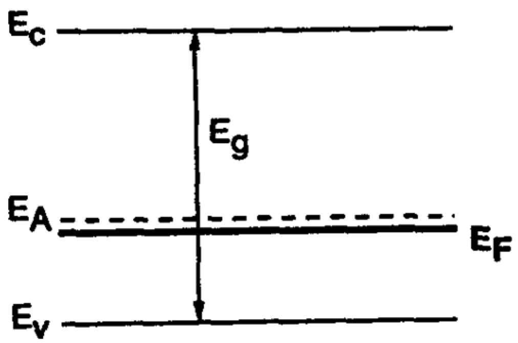
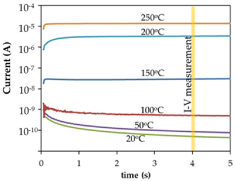
2.4. Measurement of Leakage Current Characteristics in PT-Based Materials
The leakage current reduces the overall efficiency of the pyroelectric detectors. In thin insulating films, the current depends on the applied voltage (), time (), and temperature (). A compilation of possible transport mechanisms in thin films is provided in Appendix A.1. PT-based materials exhibit different conduction behavior depending on physical parameters such as film microstructure, thickness, doping level, and electrode materials. Among different PT-based materials, PZT has been the focus of much attention due to its applicability in ferroelectric random access memory (FERAM) technology and has been prepared by the sol-gel technique almost exclusively.
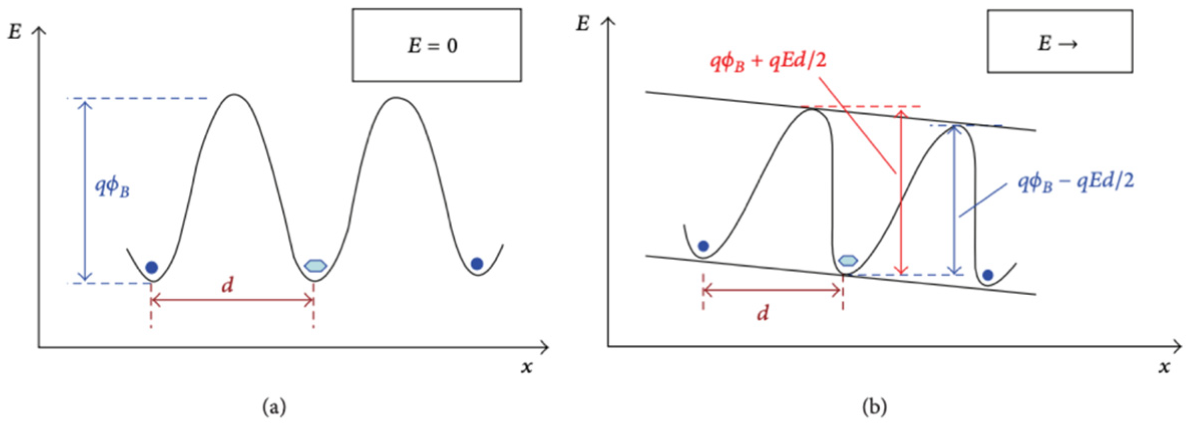
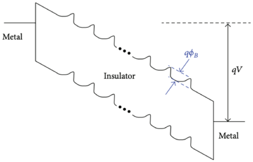
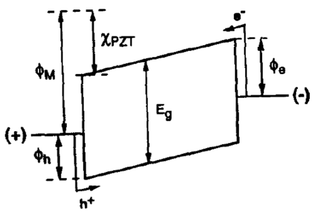
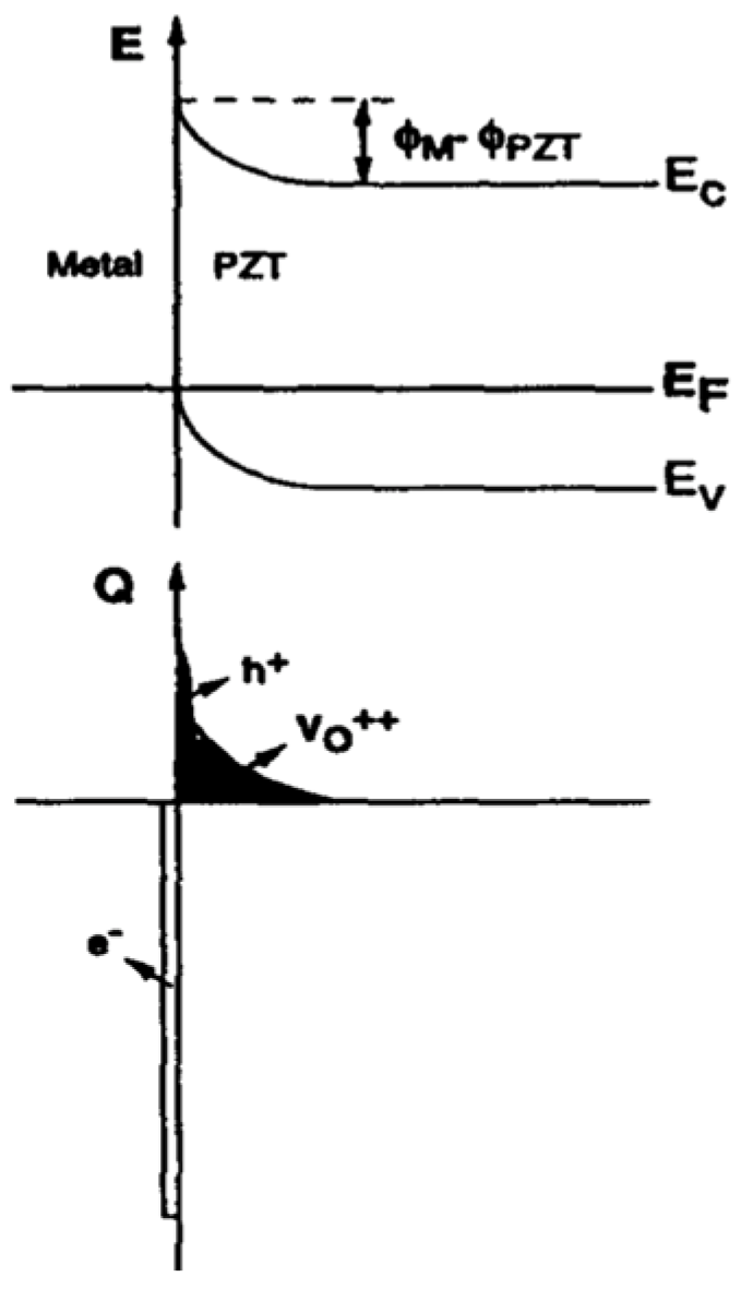
2.4.1. Metal/PZT Band Diagram
To identify leakage mechanisms in PT-based dielectric insulators, it is crucial to consider the band diagram of the metal-semiconductor (M-S) contacts. In this section, we discuss the electronic properties of PZT material. We begin with the theoretical analysis of the Pt/PZT interface.
PZT is a relatively wide bandgap semiconductor with and generally has p-type conductivity. Raymond and Smyth [22] studied polycrystalline bulk samples at high temperatures (). At such high temperatures, both grain boundary and bulk conduction may contribute to the transport mechanism. Unintentionally doped PZT possesses a large concentration of acceptor impurities but is generally compensated by the formation of oxygen vacancies (), which leads to a relatively small concentration of the active acceptors. Hence, the Fermi level () resides at energy relatively far from the valence band edge ().
Due to the large ionization energy (0.71 eV) of the acceptor impurity level (), the impurities freeze out at lower temperatures (). In this case, resides below , as shown in Figure 8. Except for the deep hole trap formed by the acceptor impurities, can act as a shallow hole trap and as a deeper (~1 eV) electron trap. These traps can influence the free-carrier conduction in PZT via Poole-Frenkel or hopping conduction [12,23,24]. Two kinds of crystalline structures are important in thin-film PZTs:
- fine-grained films, with grain boundaries (GB) parallel and perpendicular to the current flow, and
- columnar grain structures, with GBs parallel to the current flow.
Grain boundaries can act as barriers when they stand perpendicular to the current flow. These structural differences may result in a variety of I(V) behaviors. In the following analysis, to simplify the discussion, PZT film is assumed to be a single crystal material.
Below , PZT accommodates only a minute concentration of holes and thus, behaves very much like an insulator. Consequently, in a PZT ferroelectric capacitor (FECAP) with blocking contacts, a supply of carriers at the metal-PZT contacts is required if the charge is to be transported across the insulator.
Figure 9 depicts the energy band diagram proposed by Wouter et al. [22] for the structure, which predicts a hole barrier of and an electron barrier of for injection from the metal into the fully depleted PZT. Assuming PZT behaves like a fully depleted “insulator”, Pt contacts are employed and Schottky theory applies () [23]. Wouter et al. [22] argued that hole injection prevails. The electron affinity for PZT () is derived by assuming and using the experimental value of for the PZT work function [24].
At higher temperatures, oxygen vacancies (), which act as compensating negatively charged acceptors, are mobilized and drifted under the influence of the electrical field, induced by contact potential, for example [25]. These charges will then accumulate near the Pt electrode and provide the required positive space charge needed to neutralize the negative electrode charges caused by contact potential.
This process is important during the annealing of the Pt-PZT interface [26].
If the metal is negatively (or positively) biased relative to the semiconductor (PZT), the required balancing charge in the semiconductor (PZT) interfacial region is positive (or negative), which must be supplied through hole accumulation (hole depletion, i.e., ionized acceptors or inversion) and is accompanied by an upward (or downward) bending of the energy bands. For the lightly p-doped compensated PZT films, the concentration of the holes in the thin film is inadequate to support balancing charges on the electrodes. Hence, negligible band bending may occur even when a large negative (or positive) voltage is applied. As a result, in both cases, PZT will become fully depleted and behave as an ideal insulator. Since > , accumulates near the Pt contact during the annealing. Throughout the cooling down period, however, the space charge created remains frozen-in near the Pt/PZT interface. This causes the bands to bend up, as shown in Figure 10.
While the oxygen vacancies freeze-in at lower temperatures, the accumulated holes remain mobile. If this carrier reservoir can be easily refilled, either by carriers supplied by the metal (when ), or by fast carrier generation, an Ohmic contact is achieved, which enables a hole current to flow from the positively biased contact through the PZT film. At least in a low current regime, this hole current is not controlled by the interface but by the conduction process in the bulk of the PZT film.
The hole accumulation region eventually disappears if the bias is increased, and the contact returns to a blocking state, where the current will become interface-limited, and holes can only be injected into the PZT film by crossing over the barrier.
The non-annealed Pt-PZT interfaces present a poor interface, which further impedes the injection of carriers. Then, ionic conduction becomes dominant.
In contrast to bulk models, the current increase in the current-degradation regime is not caused by bulk conductivity changes but by (increased) carrier injection at the Pt-PZT interface, while either the carrier injection mechanism or bulk conduction processes may limit the current in the saturation current region.
2.4.2. Leakage Mechanisms in PT-Based Materials
Various processing steps are utilized for the preparation of PT-based thin films, which lead to different electrical properties. Consequently, numerous physical models have been proposed to describe the leakage current behavior in PZT films. A summary of the proposed conduction mechanisms in PT-based films is provided in Table 2 and has been analyzed by Wouters [22] (see Appendix A.1).
Table 2.
Summary of the proposed conduction mechanisms in PT-based films.
Figure 11 shows the typical transient, saturation (true leakage), and degradation regime, as well as the breakdown region commonly observed in I(t) characteristics of Pt-PZT-Pt capacitors. Four distinct regimes in I(t) characteristics of the Pt-PZT-Pt FECAP can be identified [27]:
- The transient current: This is the initial decrease in current with time.
- The saturation (“true” leakage), which becomes pronounced after current transients are died out and predominates leakage for a certain period.
- The resistance degradation regime, where I(t) increases until a maximum value is reached.
- The dielectric breakdown region.
Thin polycrystalline alkaline-earth titanates normally contain substantial concentrations of positively charged oxygen vacancies. Thus, in a DC electrical field, they migrate toward the cathode. This makes it easier for carriers (electrons) to overcome the barrier because it modifies the shape of the barrier. These vacancies are positively charged with respect to the regular lattice and are commonly held responsible for resistance degradation [29,39] that provides a quantitative analytical model for the resistance degradation regime.
Figure 12 shows the charging and discharging currents measured at . This sample was pre-poled with a poling field parallel or antiparallel to the applied electric field. The magnitude of I(t) depends on the sample history [22]. These observations show that the identification of the conduction mechanism (s) in PT-based films is complex. This is because:
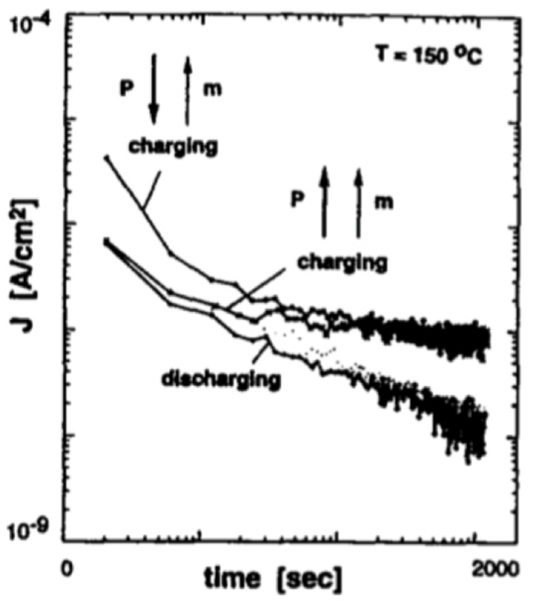
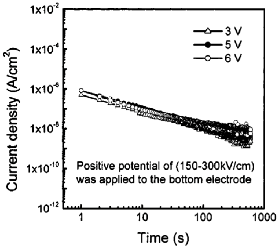
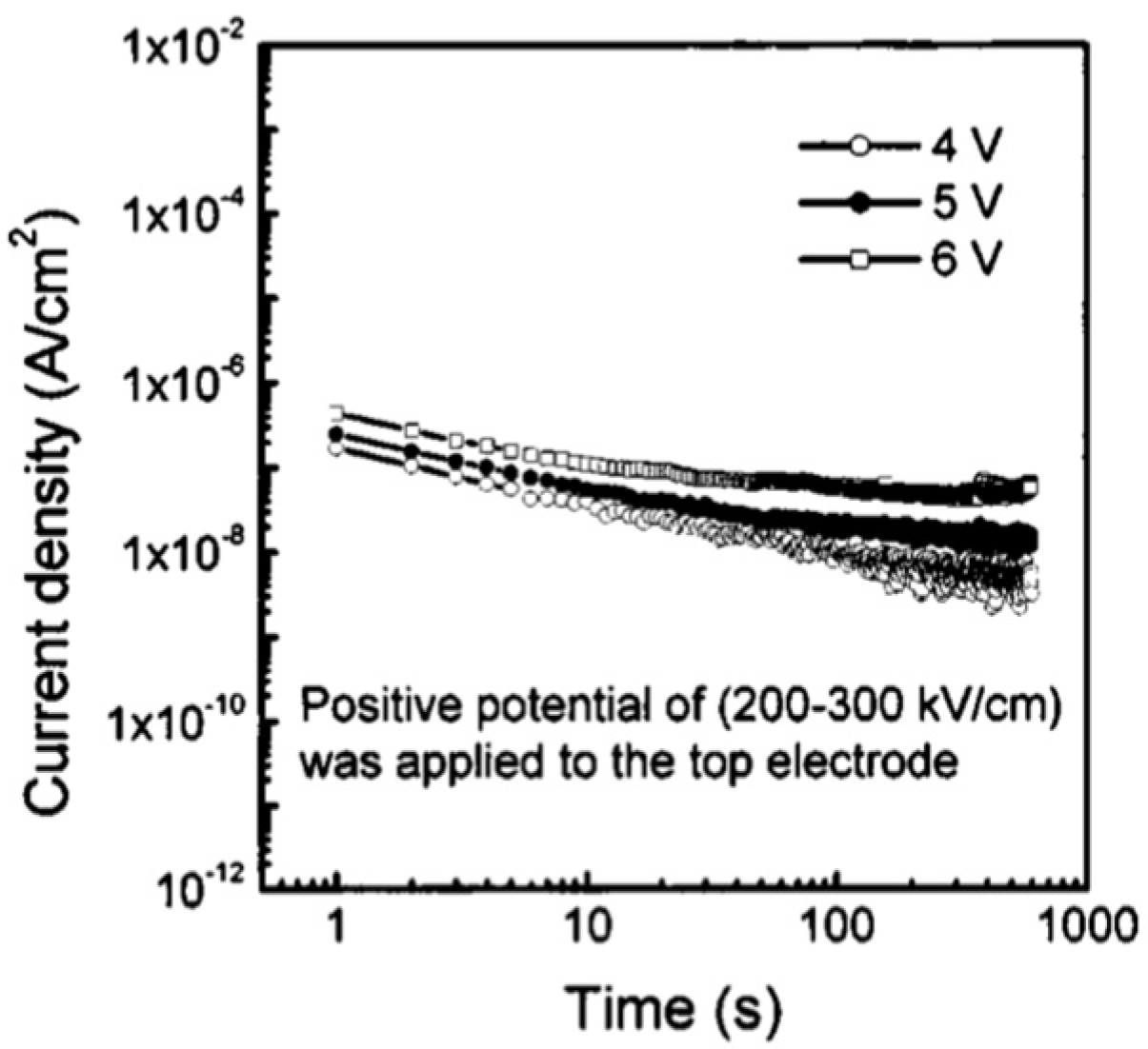
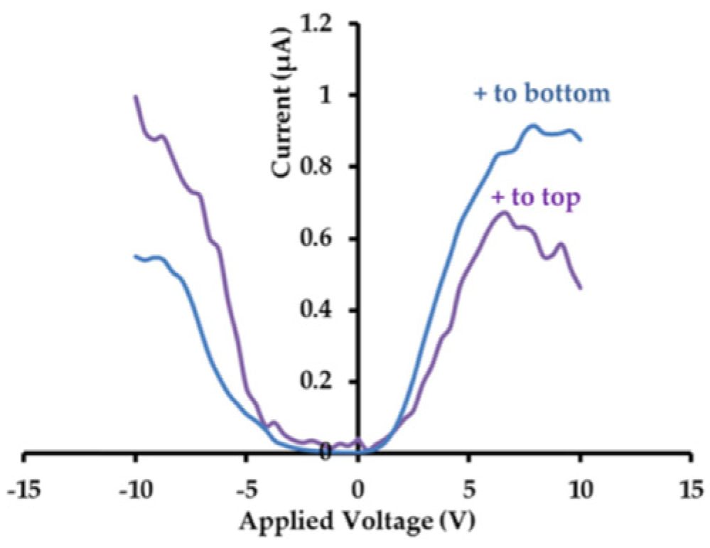
- The data on I(V) and I(t) measurements depend on the separation technique used for the “true” leakage current from the dielectric relaxation current. In perovskites, the current comprises a time-dependent component dielectric relaxation, which is strongly dependent on the measurement technique, prior history of the sample, and other factors, as seen in Figure 12.
- Often, different conduction mechanisms result in similar I(V) curves, especially when the analysis is carried out on a limited voltage interval.
- Different processing factors and physical parameters including microstructure, thickness, doping level, and electrode materials affect conduction behavior in polycrystalline films.
Thus, a comprehensive experimental study on transport mechanisms in PT-based perovskite dielectrics requires the utilization of diverse measuring techniques for samples prepared with various processing parameters such as thickness, grain structure, interface structure, and doping levels.
In the case of perovskite materials, the leakage current can be described as a superposition of two components: the relaxation current, [] which tends to vanish as the stress time is increased, and the “true” leakage current, which reflects the real evolution of leakage current inside the dielectric [22,40]. Although the true leakage current is usually considered static, it does evolve with time. To consider this time evolution, two complementary factors is introduced: the resistance degradation factor [41] and the resistance restoration factor [42].
where is the slope of in the log-log plot. becomes predominant after a certain time has elapsed [43]. There are three well-known mechanisms that can give rise to the exponential dependence of current density on the elapsed time; these are space-charge trapping, relaxation time distribution, and electrical charge hopping [44].
The precise determination of conduction mechanisms requires accurate measurements of the “true” leakage current. Measurements of and characteristics must be carried out in the saturated current regime at . The time dependency of the current density makes it challenging to obtain curves representative of the true leakage current.
- Dielectric relaxation regime.
The first term on the right-hand side of Equation (4) follows a Curie Von-Schweidler law and is due to dielectric relaxation [42]. As shown in Figure 11, it is attributed to the transient regime and characterized by the initial decrease in current due to the displacement of charges [45]. For PT-based insulators, the relaxation mechanism is pronounced at , while the term is thermally activated with an activation energy , and the slope in relaxation regime () appears to be temperature-independent, with . Several authors proposed possible mechanisms responsible for the dielectric relaxation process for PT-based materials. Chen et al. [45] attributed dielectric relaxation to either the electrical charge hopping or to a Maxwell-Wagner polarization with a wide distribution of relaxation times. Nagaraj et al. [46] assumed oxygen vacancies as well as ions as possible trapping sites and considering the energy levels of these defects in the band gap of PZT, they attributed dielectric relaxation to charge entrapment in respective trapping sites. On the other hand, Simons [47] suggested that electrons associated with oxygen vacancies account for the relaxation current.
- 2.
- The saturation region.
This is the relatively constant low-level current density component in Figure 11 and represents the true leakage current. It can be described as a thermionic Schottky injection of holes through the anode/PZT interface, which follows the relationship:
where is the Richardson constant, is the initial potential barrier height at the anode interface, and is the Boltzmann constant. This region is characterized by the fact that the charging and discharging currents are not identical [45]. Saturation is not usually a prominent component of the leakage current at room temperature even after a few . Except for small biases, it is best revealed in the temperature range of .
- 3.
- Resistance degradation and restoration region.
This is the term attributed to the increasing current region in Figure 11, next to the saturation region. The amount of increase in the current depends on the sample, which is noticeable for positively biased samples with unannealed top electrode [41] (not to be confused with dielectric breakdown). Oxygen vacancies are present in significant concentrations in alkaline-earth titanates. They are positively charged with respect to the regular lattice. In a DC electric field, they migrate toward the cathode. The redistribution of the oxygen vacancies near the interfaces alters the shape of the barrier for carrier injection, making it easier for electrons to overcome [41]. This increase in current density may be modeled by a decrease in the effective barrier height at the cathode. Zafar et al. [39] modeled this resistance degradation region by a factor as:
where represents the metal/PZT barrier height lowering [41]. The onset of this current degradation regime is shifted to shorter times with increasing temperature and voltage [41], making it difficult to distinguish the transition from the saturated current regime to the resistance degradation regime.
As the time elapsed, oxygen vacancies accumulated near the neutralized cathode. Consequently, space charge density is decreased at the cathode interface, for which electron injection may be modeled by an effective increase in the barrier height leakage, which reaches a maximum and then starts to decrease. This behavior is modeled by the resistance restoration factor [42]:
where describes the barrier height restoration potential. Then, after a certain period of stress time, the metal/PZT barrier height tends to recover its initial value due to space charge reorganization induced by lead vacancies.
To investigate the conduction processes, measurements of the I(V) and I(t) characteristics should be carried out in the saturated current regime () [41].
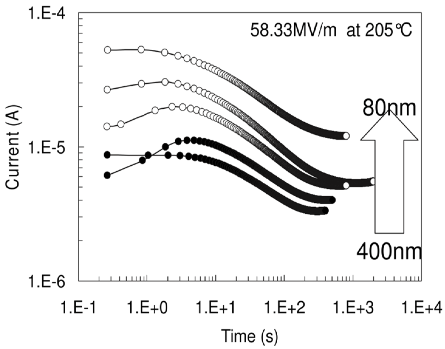
2.4.3. The Effect of Dielectric Thickness on Leakage Current Mechanisms
Chentir et al. [27] investigated the evolution of leakage current in PZT capacitors as a function of dielectric thickness. A protocol was introduced, which avoids artifacts commonly encountered in the measurement of current in perovskite dielectrics (Appendix A.4). A change in leakage current mechanism from Schottky to Poole–Frenkel (PF) mechanisms (Appendix A.3) was observed as PZT thickness decreased and was accompanied by a drift in the value of the device capacitance. Modeling the capacitor as in Figure 13 provides an estimate of nm thickness for the “dead layer”, although the nature of such layer has long been a matter of much controversy [29,48]. The switch from an interface-limited conduction mode to a bulk-limited mode is attributed to the presence of a higher defect concentration due to oxygen vacancies (in comparison with PZT bulk) in the dead layer present at PZT-electrode interfaces.
Figure 13.
Schematic representation of three series capacitors modeling for dead layer thickness extraction [27]. Reprinted from [27], Figure 5, Figure 7, Figure 8 and Figure 14, with the permission of AIP Publishing. https://doi.org/10.1063/1.3055416.
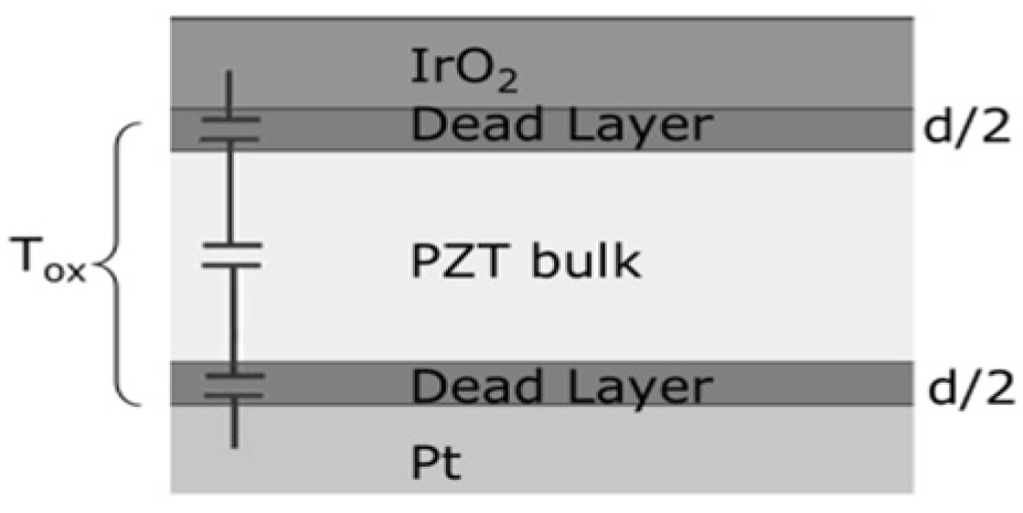
2.4.4. Case Study: Leakage Current Mechanisms in Au/PCT/Pt Structure
Tang et al. [3] measured the room temperature characteristics of the structure under different applied DC voltages (with the positive or negative potential connected to the Pt and maintained for ). The dielectric relaxation current versus time characteristics of the capacitor was measured after removal of the field.
Figure 14 shows the current density as a function of voltage with Pt electrode biased at . At low electric fields with negatively biased electrodes, the interface exhibits a Schottky barrier characteristics, while the Au/PCT interface forms an Ohmic contact. This explains the dependence of leakage current density on the bias polarity.
As shown in Figure 15, when the Pt electrode is biased negatively, the interface forms an Ohmic contact for . Schottky emissions over the barrier dominate when .
Figure 16 indicates that an Ohmic contact is formed when , while the current obeys SCLC behavior (when ) and the voltage range of marks the region where conduction mechanism is transformed from Ohmic to SCLC. The trap-filled limit voltage is . The dielectric relaxation current behavior of capacitor conforms to the universal (Curie–von Schweidler) law at a low electric field. At higher fields, the current has contributions from both a dielectric relaxation current and a leakage current.
Figure 16.
vs. plot when the Au electrode of the thin-film capacitor is negatively biased. The conduction current shows space-charge-limited behavior for when the Au electrode is negatively biased [3]. Reprinted from [3], Figure 2, Figure 3, Figure 4, Figure 5, Figure 6 and Figure 7, with the permission of AIP Publishing.
Figure 17 depicts the for several bias voltages applied to the bottom Pt electrodes. The currents measured at low fields (150 and 250 kV/cm) indicate the contribution of pure dielectric relaxation currents.
The dielectric relaxation current behavior of Au/PCT (24)/Pt capacitor obeys the Curie–von Schweidler law at low electric fields, with and at and , respectively. Similarly, when positive potential is applied to the bottom electrode at low fields, indicates the contribution of pure relaxation current (Figure 18). While at higher fields (250 and ), the current has contributions from both a dielectric relaxation current and a leakage current, which itself comprises effects of oxygen vacancy concentration, the magnitude of polarization, space charge trapping, electrical charge hopping, and/or the contribution of defect-dipole complexes.
2.5. Measurement of Fatigue in PT Based Materials
Considerable disagreement exists in the literature regarding fatigue mechanisms in Pt/Pb (Zr, Ti)/Pt (Pt/PZT/Pt). Dimos [49] attributed fatigue to domain pinning, while Desu et al. [50] corelated fatigue to the space charge. Conductive oxide electrodes are known to improve fatigue properties of FE memory devices. When Pt electrodes are replaced by oxide electrodes such as Ru, SrRu, and (La, Sr) Co(LSCO), the capacitors show excellent fatigue and imprint properties [51,52]. It has been proposed that oxide electrodes act as sinks for oxygen vacancies, thereby eliminating fatigue. To understand fatigue and degradation mechanisms in Pt/Pb (Zr, Ti)/Pt (Pt/PZT/Pt) heterostructures, Nagaraj et al. [26] investigated leakage current mechanisms in lead-based thin-film FE capacitors. Distinct differences exist between the electrical behavior of Pt/PZT and LSCO/PZT capacitors, which may stem from their interface disparities. Leakage in Pb based perovskite-type titanates Pb (Zr, Ti) thin films has been previously investigated [37]. Studies on Pt/PZT/Pt structures reported Schottky emission with a barrier potential of 1.41 eV [45,53,54].
Nagaraj et al. [26] prepared epitaxial (La, Sr) Co/Pb (Zr, Sr) /(La, Sr) Co capacitor structures to investigate the dominant leakage current-voltage, I(V) and the behaviors of such capacitors. Epitaxial growth of (La, Sr) Co was purposely utilized to eliminate the effects associated with grain boundaries. It has been established that PZT and PLZT capacitors show Ohmic conduction at low fields (10 kV/cm), with a slope of nearly 1 (Figure 19). The I(V) curves are (i) nearly symmetric, (ii) dependent on temperature, and (iii) possess a positive temperature coefficient (TC).
Figure 19.
(a) I-V-T plots for a typical LSCO/PZT/LSCO capacitor showing nonlinear I-V characteristics and positive TC current. (b) plot for a typical LSCO/PZT/LSCO capacitor showing linear trend at fields higher than V/cm [26]. Reprinted from [26], Figure 2, Figure 3 and Figure 5, with permission from the American Physical Society.
I(V) is nearly symmetrical but nonlinear at higher fields and temperatures. Figure 20 shows the plots at different temperatures. A linear relationship is detected at high temperatures and fields. From the slope of these curve, is obtained for the PZT and PLZT films. This behavior also suggests that at high fields and temperatures, conduction is dominated by field-enhanced thermal ionization of trapped carriers (i.e., Poole-Frenkel emission). Figure 21 shows the plot of voltage versus thickness (V-d) at a constant current in the LSCO/PZT/ LSCO capacitor. The linear trend indicates a uniform field in the bulk of PZT.
The fact that the electric field is uniform in the FE film and that both temperature and field activate the current further confirms that PF emission is responsible for the transport mechanism. The trap ionization energies calculated from the slope of lnσ_0 versus 1/T plots are in the range for PZT and PLZT capacitors. This suggests that the same trap center acts as the P-F center in both PZT and PLZT films. The fact that the ionization energy of to is 0.5 eV suggests that could be the possible PF center. No space-charge region is created at the (PZT or PLZT)/LSCO interface. This could be the reason for good fatigue and imprint characteristics in these capacitors.
Bouyssou et al. [55] investigated the reliability properties and the degradation mechanisms in the Ir/Pb (PZT)/Pt capacitors by characterizing leakage current conduction and provided a model for the evolution of current in the Ir/PZT/Pt capacitor as a function of time, voltage, and temperature.
The leakage current conduction in Ir/PZT/Pt structures was found to be controlled by the energetics of the barrier height at the cathode interface. Hence, the voltage and temperature evolution of leakage current were interpreted as an interface-controlled thermionic injection of carriers over a potential barrier at the cathode/PZT contact. The time evolution of the leakage current is mainly characterized by the resistance degradation phenomenon. The model is based on the redistribution of oxygen vacancies near the cathode interface, but also includes the role of oxygen vacancies on dielectric relaxation and trapping phenomena.
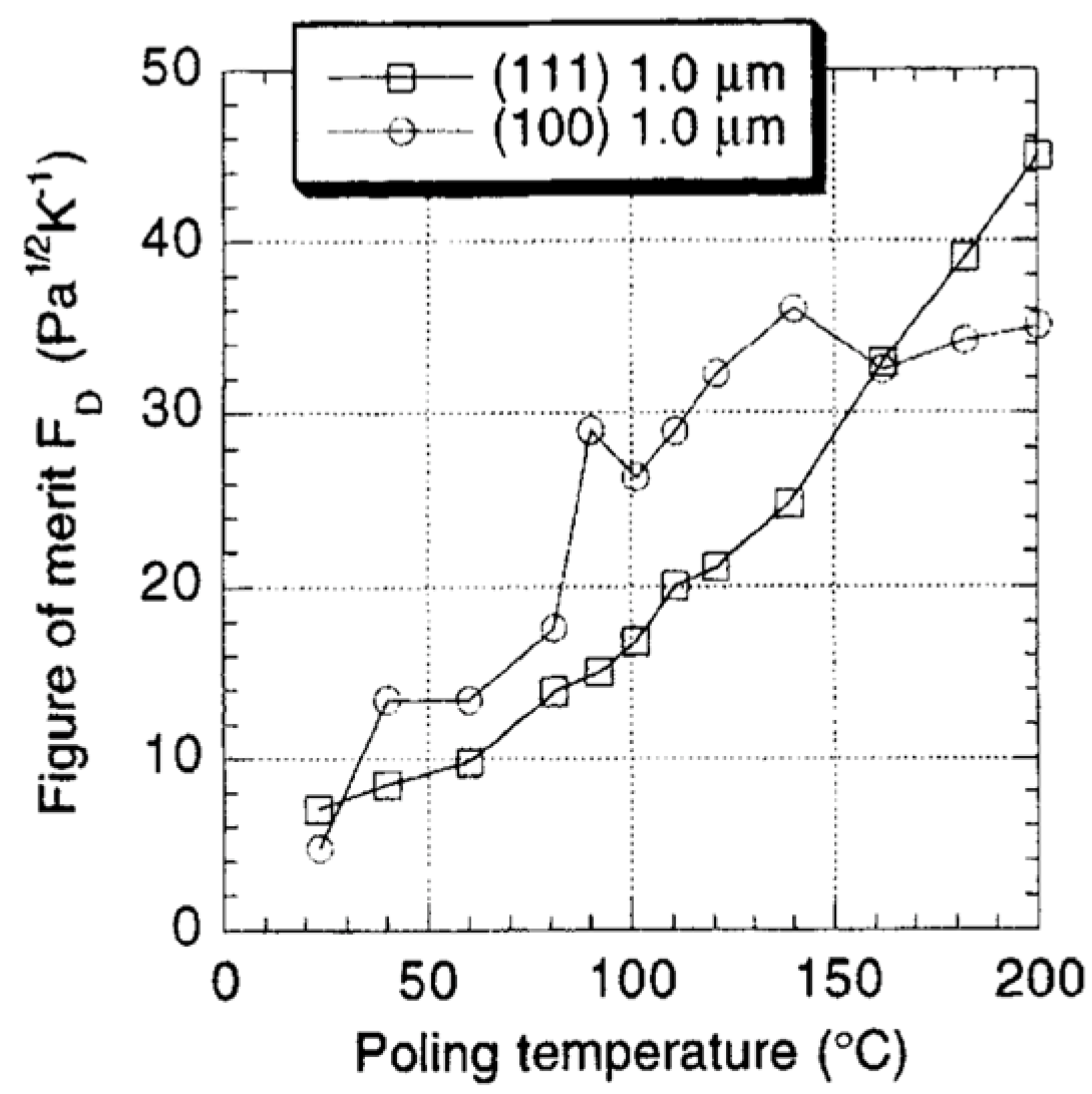
2.6. Poling of Pyroelectric Thin Films
Poling is the process carried out to achieve maximum possible FE polarization parallel to an external electric field. During this process, domains with a favorable polarization direction are encouraged to grow at the expense of domains with unfavorable directions. In an unpoled polycrystalline thin film, most grains have an unfavorable crystallographic orientation which prevents the polarization direction to attain a direction perpendicular to the substrate plane and hence leads to a reduction of the maximum.
Once poled, an FE sample will remain poled unless it is de-poled, via repetitive heating and cooling through its transition temperature.
Kohli et al. [56] studied poling conditions for <111> oriented Pb1−xCaxTi(PCT), with as well as <111> and <l00> oriented PbZrTi1−xTi, with (PZT 15/85) thin films. Ca addition to PbTi decreased the tetragonality of the unit cell and thus reduced the Tc, which in turn resulted in higher pyroelectric coefficients. Kohli et al. [56] also used the controlled heating-rate technique [57] to achieve reduced values for dielectric permittivity for the PCT15 by controlling porosity by adjusting nucleation and growth of their sol-gel grown films.
The effect of poling temperature on p and at a constant field of 250 kV/cm is shown in Figure 22. In both films, the pyroelectric coefficient increases with the poling temperature, whereas the permittivity as well as the dielectric loss tangent decreases.
Figure 22.
Permittivity and pyroelectric coefficient as a function of the poling temperature for (111) oriented PZT 15/85 thin films. The films were poled at 250 kV/cm for 10 min [56]. Reprinted from [56], Figure 1, Figure 3, Figure 4 and Figure 5, with permission from the Copyright Clearance Center Inc. (CCC) on Taylor and Francis’s behalf.
Two figures of merits are of interest: one for voltage response , favoring a high pyroelectric coefficient p and a low permittivity and the other for detectivity , which, in addition, requires a low . Figure 23 depicts the voltage figure of merit versus poling temperature (poled at 250 kV/cm) of (111) and (100) oriented PZT 15/85 thin films.
Optimization of the poling temperature and the electrical field leads to improvement, as shown in the figure of merit for voltage and detectivity. Due to a significant reduction in the dielectric constant of porous films, values of Fv are 3X higher in PCT than in PZT thin films, which suggests that PCT is an excellent candidate for pyroelectric applications. Figure 24 shows that detectivity () versus poling temperature (poled at 250 kV/cm) of (111) and (100) oriented PZT 15/85 thin films 180 domains contribute to phase instability. Thermal activation helps to avoid obtaining such domain configuration.
Figure 25 depicts the changes of the pyroelectric coefficient, the permittivity and the figure corresponding to voltage for the PCT15 as a function of poling electric field. Poling was performed at 170 °C for 10 min. Pyroelectric coefficient is seen to steadily increase, reaching a plateau at about 600 kV/cm, which can be attributed to the continued switching of 90°- and/or 180°-domains. The permittivity measured after poling remains approximately constant for all electric fields; thus, remains constant when changes. The necessary poling fields are high compared to PZT, which may be due to the small grain size of about 55 nm for porous PCT15. Domain wall motion and thus polarizability is known to be significantly reduced in small-grained material [55,58]. The dielectric breakdown strength for films of all compositions was equally high and occurred after about 5 min at 160 °C between 1 and 1.5 MV/cm.
Hot poling reduces a-domain population in <100> oriented PZT thin films. At high temperatures, the mobility of oxygen vacancies increases such that it can migrate even under small electric fields. The oxygen vacancies combine with lead vacancies as well as other impurities like , and to form defect dipoles that interact with the domain walls [59]. The defect-dipole complexes reorient themselves under an applied field [60].
The FE domain configuration is frozen during cool-down to room temperature and the polarization is stabilized. The domain pinning by defects leads to a large internal field of 140 to 180 kV/cm (imprint) [56,61]. After poling, some of the poled domains may switch back due to phase instability. Back switching reduces the polarization, and as a result, the pyroelectric signal decreases with time. High coercive field materials with good retention are thus better candidates for pyroelectric applications. Interestingly, these materials also offer comparatively lower dielectric constants.
The decrease in the and after the poling process is attributed to the elimination of domain walls by the internal field (Figure 25). As the DC-poling field increases, the dependence of and on the AC-field drops compared to the unpoled state. This is because domain walls are removed. Hence, the wall contribution diminishes. The combination of these phenomena with porosity and an increased pyroelectric coefficient from Ca-addition result in an improved figure of merit.
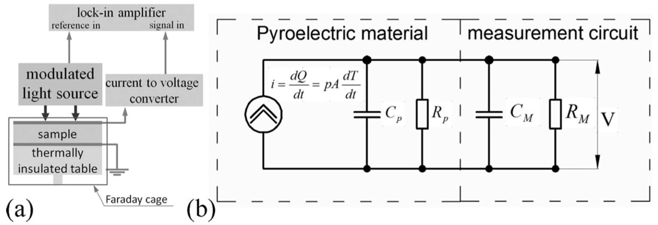
2.7. Pyroelectric Measurement
It has already been shown that temperature changes in some crystals (e.g., perovskites) modify the magnitude of their permanent dipole moments or their polarization. This phenomenon is referred to as “pyroelectricity”, which may arise from one or more of the following sources [62]:
- Changes in the permanent polarization along the x direction ,
- Changes in dielectric permittivity of medium leading to the electric field induced polarization ,
- Changes in the piezoelectricity , and
- Changes in the flexoelectric polarization .
Therefore, the changes in the polarization along x axis is described by:
where is the permanent polarization along x axis, represents components of the dielectric tensor, represents the electric fields in the k directions, represents components of the piezoelectric tensor, represents components of the stress tensor, represents the components of the flexoelectric tensor, and represents the components of the strain tensor. This 1D analysis can be generalized to 2D or 3D without any loss of generality. By dividing both sides by incremental changes in temperature (ΔT) and considering the limiting case, where ΔT⟶0, the following equation is obtained:
Thus, the pyroelectric coefficient is calculated as follows:
where . When a field is applied externally, the second term in (10), may become enormously large in the vicinity of phase transitions, where becomes very large [63].
This criterion is implemented for the device operation in the “dielectric bolometer mode”. It must be noted that as the electric field increases, decreases, and thus, the second term in (10) remains finite. Nevertheless, it is undesirable for pyroelectric detection because it obscures the pyroelectric effect. The effect of the flexoelectric term, although considerable at the nanoscale [64], where large strain gradients are present, is neglected in the present treatment.
2.7.1. Measurement of the Pyroelectric Effect
There are three main approaches to the measurement of the pyroelectric effects on bulk samples: (1) direct measurement of the polarization and/or dielectric constant at two or more fixed temperatures, (2) measurement of the pyroelectric current induced by a ramping temperature up (or down), and (3) measurement of the pyroelectric current induced by periodic temperature change. These are briefly discussed below:
Direct Measurement of the Polarization and/or Dielectric Constant at Two or More Fixed Temperatures
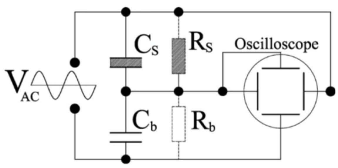
- A.1. Sawyer-Tower (ST) Bridge Technique
Ferroelectrics can reverse the direction of their spontaneous polarization under the influence of an external electric field and hence allow the direct measurement of the magnitude of the permanent dipole moment. In the ST technique [65,66], the polarization and/or dielectric constant of the material is directly measured at two or more fixed temperatures, and the pyroelectric coefficient is obtained from . The method is restricted to ferroelectrics, where coercive fields are much smaller than their breakdown fields. The currents are evaluated by running the ST bridge as shown in Figure 26.
Figure 26.
The Sawyer-Tower bridge. In its original form, it did not consider the presence of the leakage current represented here by . This current must be partially balanced by a shunt resistor and polarization hysteresis curve must be checked. A properly balanced would show a square-shape polarization hysteresis loop. The capacitance of the material is denoted by . The bridge is constructed using a linear capacitor [62]. Reprinted from [62], Figure 1, Figure 2, Figure 3, Figure 4, Figure 5, Figure 6, Figure 7, Figure 8 and Figure 9, with the permission of AIP Publishing.
There are three main approaches to the measurement of the pyroelectric effects on bulk samples.
The analysis above assumes that polarization (P) is perpendicular to the plane of the contacts. If P makes an angle Ω with respect to the to the plane of the contacts, this technique provides the projection of the polarization on the plane of the contacts, . The bridge is generally constructed using a linear capacitor (), where and is the capacitance of the FE material, which includes polarization switching . Here, the sample area is denoted by . The voltage measured across is proportional to the total surface charge on , which represents the polarization charge stored on the surface of the FE material in the absence of a real electric current in the FE medium. Most FE media exhibit ohmic conductivity and/or charge trapping effects. The Ohmic conductivity can be partially compensated for by shunting by resistor, whose value is varied until an ideal square polarization is achieved.
P(E) exhibits an ‘S’ shape rather than a rectangular contour if the coercive field is not uniform over the volume of the medium under investigation. It is then impossible to distinguish between Ohmic conductivity and true polarization effects. Because no value of the shunting resistor exists for which the hysteresis loop becomes rectangular. Then the ST bridge, using a shunting resistor, becomes unreliable for accurate determination of the polarization. This reservation also applies to a variation of the ST bridge, in which is replaced by a current-to-voltage converter, whose output is either electrically or “computationally” integrated and allows for extraction of the polarization and coercive field; this has become a popular ST bridge technique in industry [67].
A second issue associated with ST bridge measurement is due to charge trapping at the contact-sample interface or, sometimes, in the bulk of the medium and leads to real current components. In this case, no technique based on measuring the reversible charge storage using an alternating electric field will produce meaningful data (an example of such FE-like behavior is electret [68]. The ST technique is prone to inaccuracies stemming from the Ohmic conductivity as well as noise currents caused by interface/bulk trapped charges and is appropriate only for ideal pyroelectric materials with square hysteresis loop.
- A.2. Modified ST bridge (Liu) method
This method assumes that the loss (trap) current () is a function of the applied voltage and only the displacement current is proportional to . Liu [69] proposed a similar method that allows the extraction of the polarization and coercive field. The total polarization P* is the sum of the permanent polarization , and the polarization induced by the electric field , where is the sample thickness.
In this method, the currents are evaluated by running the ST bridge with a triangular-shaped voltage input at two closely spaced frequencies. To ensure that complete switching of the polarization takes place between applied voltages, amplitudes of the two input voltages chosen are larger than Vc. (Figure 27).
By integrating the current difference at the same voltage of the two voltage wave forms, it can be shown that:
Equation (11) is useful when polarization switching, rather than the externally applied voltage, dominates the current. This condition is fulfilled when the coercive field is small. By calculating at two different temperatures, one can evaluate the sum .
Furthermore, is determined by evaluating at .
Another technique is based on the use of an AC bridge to measure ; then, is written as:
The measurement of provides a simple means to verify the presence of ferroelectricity in bulk materials since its value is independent of frequency up to the GHz range, at least in the case of “ideal” FE material. The drawback to capacitance measurement by an AC bridge is that it always comprises artifact components due to displacement, ohmic, and charge-injection currents. The latter not only contributes to the inaccuracy of the capacitance measurements but also affects the electric field in the sample.
Measurement of the Pyroelectric Current Induced by Ramping Temperature Up (or Down)
The continuous temperature ramp technique measures the current flowing between two contacts on a pyroelectric sample induced by continuous heating or cooling. Although the thermal diffusion coefficient () for most pyroelectric materials is quite low (0.01–0.1 cm2/s), even very rapid heating rates (~1°K/s) does not lead to inhomogeneous heating of the unclamped samples. Thus, the sample is uniformly heated and hence, only the first two terms in (10) will contribute to the change of polarization. The effective pyroelectric coefficient is obtained by using two measurement techniques: (1) measuring voltage as suggested by Lang and Steckel [70], and (2) measuring the current flowing under short circuit conditions according to Glass [71] and Byer and Roundy [72].
- B.1. Measurement of the pyroelectric voltage developed across the film by ramping temperature up (or down):
Lang and Steckel [70] described the following method for measuring the pyroelectric coefficient, DC dielectric constant, and volume resistivity of lead-zirconate-titanate ceramic over a wide temperature range. The technique is based on the observation of the capacitive charging of a pyroelectric sample by the pyroelectric current generated during a continuous temperature change.
Figure 28 depicts the equivalent circuit for the pyroelectric device, along with its measurement circuit. Assuming that the polar axis is normal to the sample electrodes, the method then leads to , and being parallel to the polar axis. The circuit of Figure 28 is shown below:
where is the equivalent (total) capacitance of the pyroelectric element and the electrometer , and is the equivalent (total) resistance of pyroelectric element , and the shunt resistance (external to sample).
Figure 28.
Lang and Steckel measurement circuit [70]. Reprinted from [70], Figure 1, with the permission of AIP Publishing.
Assuming that the time constant characterizing the rate of temperature change of the samples is much greater than , the integration of (13) with the initial condition gives:
Here, represents the time derivative of the temperature at . The method is easily realizable using a temperature-controlled table. Since the sample temperature is directly measured, can be determined for uniformly heated samples by measuring with at least two different shunt resistors . This technique does not require measurement of heat flux that does not attain isothermal conditions and does not alter the domain structure of a FE material. However, it does require prior knowledge of conductivity as a function of temperature and is a suitable alternative when does not hold.
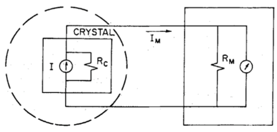
Measurement of the Short Circuit Current Produced by a Continuous Temperature Ramping (Up or Down)
Figure 29 shows the equivalent circuit for DUT that is connected to an ammeter, which was used in [70,71,72] to directly measure pyroelectric current from
where is the pyroelectric coefficient, is the polarization, is the crystal leakage resistance, and is the ammeter input resistance. The measured current is given by:
Figure 29.
Measurement apparatus equivalent circuit [72]. Reprinted from [72], Figure 1, with permission from the Copyright Clearance Center Inc (CCC) on Taylor and Francis’s behalf.
As long as , gives an accurate estimate of the pyroelectric current (denoted by in Figure 29).
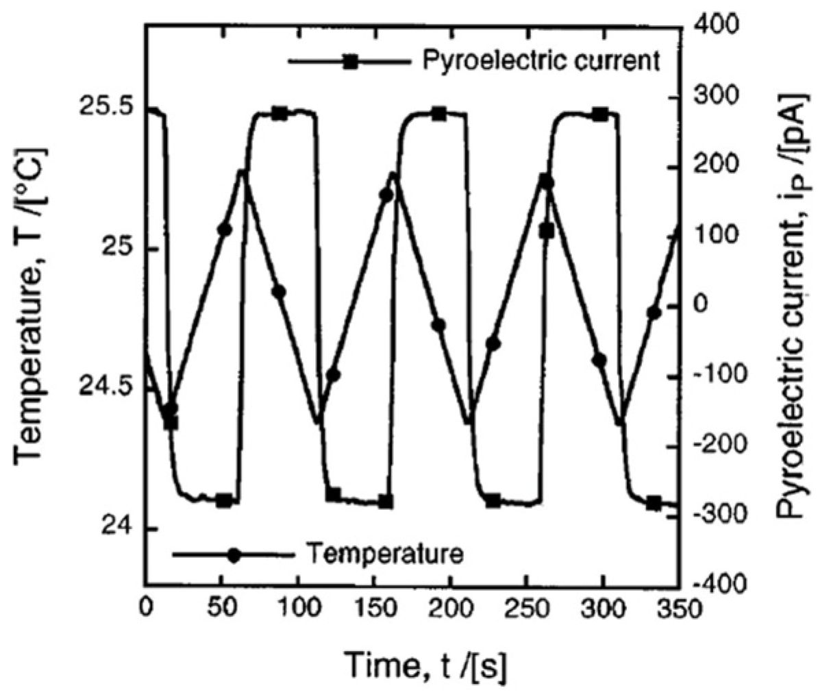
Temperature Oscillation (Dynamic) Method
This method was utilized by Davis et al. [73] to measure the pyroelectric coefficient of a thin- plate specimen using the apparatus described by Daglish [74]. The sample temperature is cycled at a frequency of 10 mHz over 1 °C. Using a Peltier element, a triangular temperature wave is formed. The current between the two electrodes is then recorded and the value of p is calculated via (27). A typical temperature waveform as well as resultant pyroelectric current is shown in Figure 30. This technique is simple and direct and does not require prior knowledge of conductivity as a function of temperature. The sample is poled once and then, a series of limited temperature runs is performed at T < Tc. Repeated oscillations over a finite temperature range will eventually deplete the traps [73].
Figure 30.
An example of the dynamic time ramping technique used to measure the pyroelectric coefficient of a single crystal (a Peltier element run at 1 mHz during a 16 min 40 s period was used to create the saw-tooth temperature profile with an amplitude of 1 degree) [62]. Reprinted from [62], Figure 1, Figure 2, Figure 3, Figure 4, Figure 8 and Figure 9, with the permission of AIP Publishing.
Since , the primary unclamped pyroelectric coefficient is obtained from (10) (see Appendix A.3). However, following issues remain:
- Creation and measurement of a large (dT/dt) with low noise.
- Thermoelectric effect is due to contacts which contribute to measured current.
- Thermally activated current due to non-uniformly distributed charged traps [75] is indistinguishable from and may dominate, especially in the poled ferroelectrics. Depletion of the traps requires a large number of repetitions (e.g., in electrets).
- Very long trap time response.
- Measurements of the current through a short circuit require (for all Ts).
In case of thin films, the following obstacles further complicate the measurement of pyroelectric coefficient:
- Depending on their preparation details, thin films generally contain pinholes which decrease the “apparent” resistivity of the sample.
- When the trap concentration , where is the trap concentration in the bulk, it is possible that , where is the pyroelectric current.
- It is possible that the current due to the thermoelectric effect .
Periodic temperature change techniques can be divided into two categories:
- Periodic pulse techniques, and
- The continuous oscillation method.
- C.1. Temperature Changes Using Periodic Pulse Techniques
Chynoweth [76] used a periodic step-like heating from a modulated IR laser, which was focused on the thermally insulated sample. A schematic of the instrumentation is given in Figure 31a.
Figure 31.
(a) Scheme of the set-up for the basic Chynoweth method, and (b) an example of the pyroelectric current measured with the Chynoweth technique. The sample is 0.2 × 0.2 μm wide, 0.4 μm thick self-supported film of BaTi tethered to a Si substrate [62]. The top and the bottom contacts are of Ag and account for more than 90% of the heat loss. The inset shows a full period (laser on and off, 666 Hz); the main panel shows an exponential fit. The film was irradiated by an IR laser (λ = 1310 nm) with a flux of 3 mW/mm2. Note: for a self-supported film, a lump model is applicable, and the heating and the cooling processes are fully symmetric [62]. Reprinted from [62], Figure 1, Figure 2, Figure 3, Figure 4, Figure 8 and Figure 9, with the permission of AIP Publishing.
Large pyroelectric currents in response to very small temperature variations is possible if a modulated IR laser is employed as the heating source since, in this case, warm-up and cool-down rates can be much larger than the those in temperature ramping techniques. This technique relies on the following two assumptions:
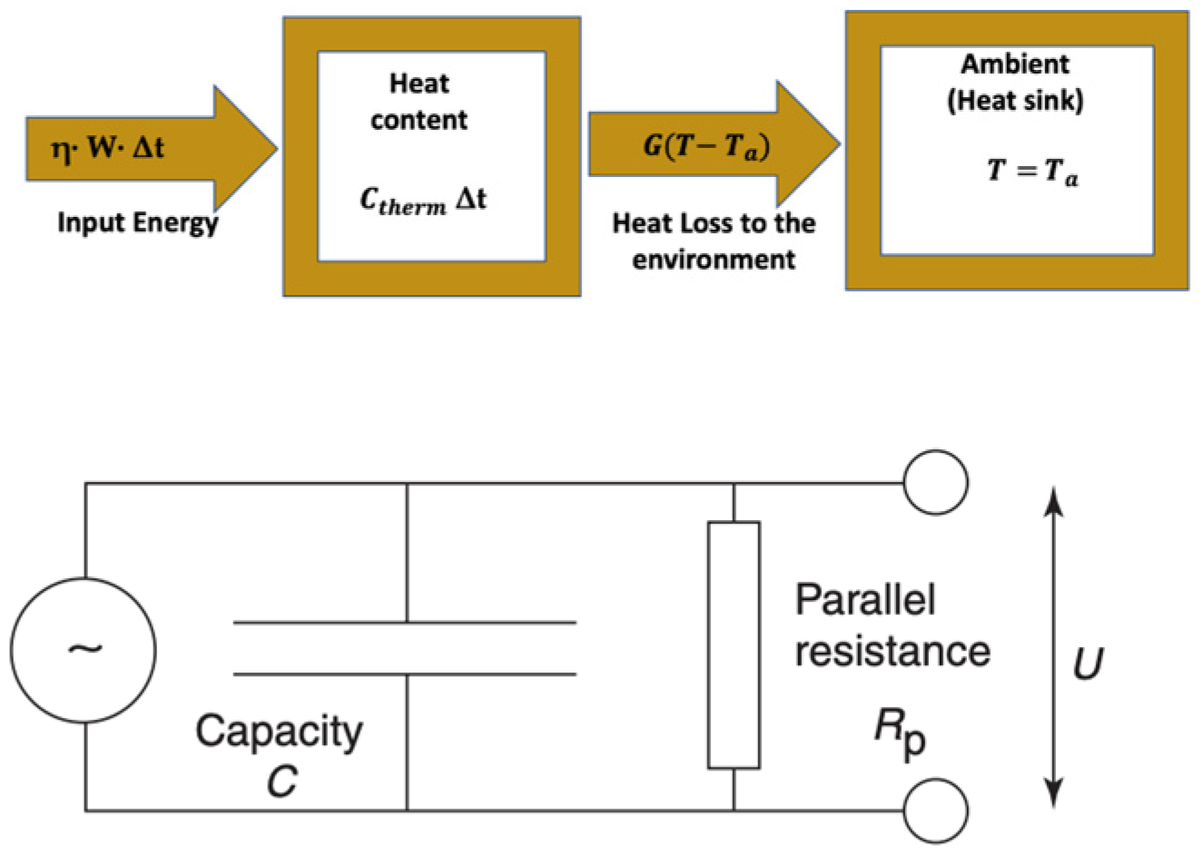
- A lump model can be devised for the DUT (Figure 32). Accurate prediction of the pyroelectric device behavior under broad range of frequencies requires distributed parameter modeling of the thermal gradients. However, if temperature differences within the DUT are much smaller than the temperature changes induced by the input energy (where, is the fraction of absorbed IR power, is the input power, and is the duration period), a reasonably accurate lumped parameter modelling approach is also possible to create. This requires identification of the thermal capacitance and heat conductance to the environment for the DUT if temperature differences within the DUT are much smaller than the temperature changes induced by the input energy. Otherwise, one can introduce “pseudo-lumped” parameters if the temperature rise and fall obey the following:
Figure 32. Lump model for a pyroelectric IR detector: schematic diagram of the thermal model and electrical equivalent circuit of a pyroelectric detector. Upon absorption of fraction of IR radiation (power ), the sensor temperature increases by , which may be obtained from the heat flow balance. The temperature change for a given amount of heat input depends on the heat conductivity to the surrounding environment assumed at temperature , the heat capacity of the element. For a thin film structure uniformly illuminated by the IR radiation, it is generally safe to neglect thermal wavelength effects and assume that the element retains a uniform temperature. Reprinted from [77], Figure 5, with permission from Elsevier.
Here, is the characteristic thermal time constant, and the maximum temperature is , where , with detector area in the input flux [62].
- 2.
- The recording of the pyroelectric current transients and averaging of the output signal is possible over many cycles to improve the signal to noise ratio (SNR).
As schematically shown in Figure 31, the modulated IR laser capable of providing a few mW of power is directed onto the sample. The pyroelectric current generated from the sample is then fed to a current-to-voltage converter and the voltage is recorded using an averaging oscilloscope. Chynoweth [76] modeled DUT as a homogenously heated body with a heat capacitance, connected to its surroundings via . As seen in Figure 31b, the pyroelectric current decays exponentially with time and the response to “radiation on” and “radiation off” is symmetric. is determined from the decay wave form. If voltage is measured, both the and the electrical time constant are obtained and if is known, the only unknown parameter is the amount of radiation being absorbed by the sample.
For bulk samples both the measurement of the and the derivation of the pyroelectric current () generated in response to the periodic heating is relatively simple. For the case of thin films, is found from an analytical solution. With this method, electromechanical isolation of the sample from noise is feasible. Thus, the sensitivity is improved. Also, the effect of trapped charges is detectable [62].
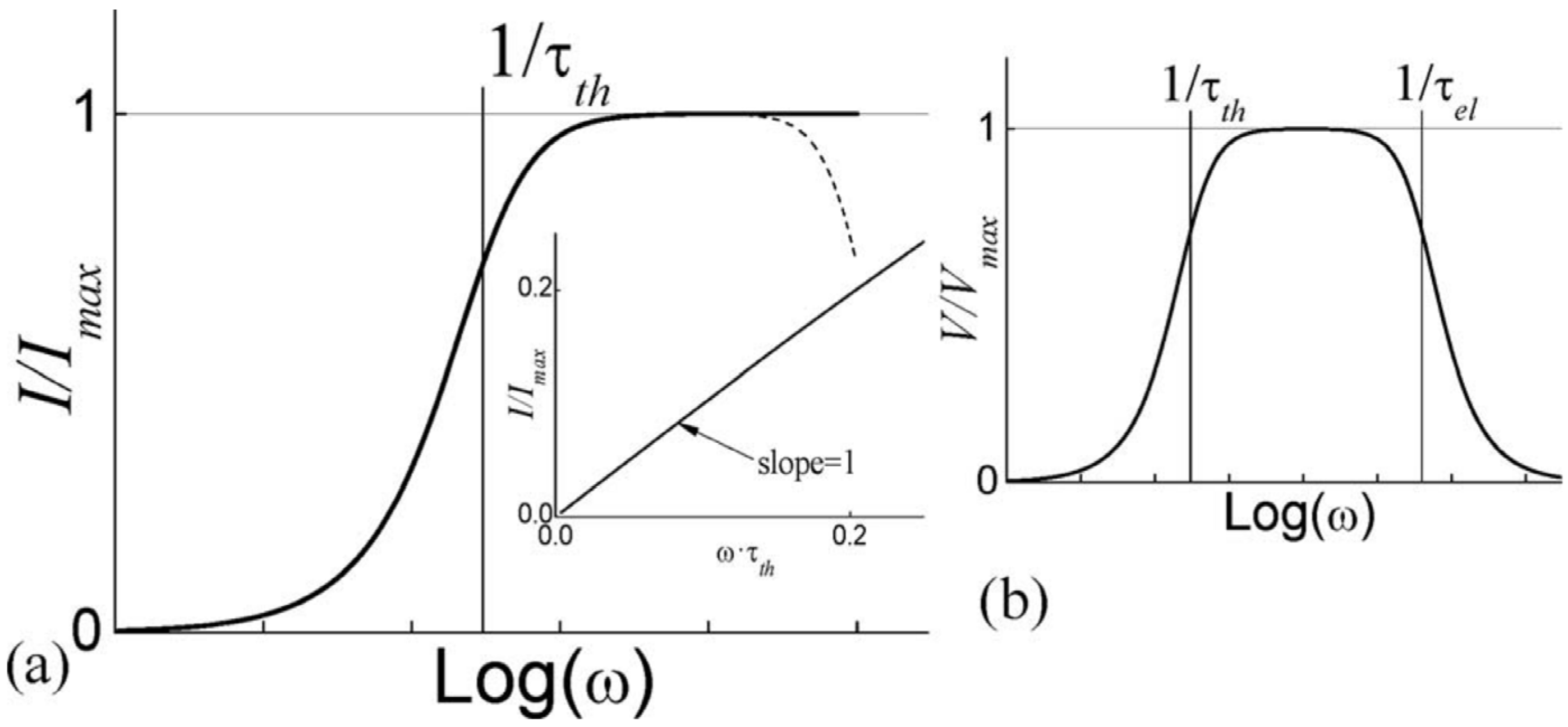
Temperature Change Using Continuous Oscillation Method
In this technique, the sample is subjected to a continuous, sinusoidally modulated heat source (typically a modulated laser), and the generated current or voltage is recorded with a phase sensitive device (typically a lock-in amplifier). The lock-in technique provides a good signal to noise () ratio for a single frequency component (Figure 33).
Figure 33.
(a) The instrumentation diagram for the continuous temperature oscillation technique, and (b) the equivalent electrical circuit with the pyroelectric material and a high-impedance voltmeter connected in parallel [62]. Reprinted from [62], Figure 1, Figure 2, Figure 3, Figure 4, Figure 8 and Figure 9, with the permission of AIP Publishing.
If the sample can be modeled by the lumped parameter approach, the derivation of the current generated in response to the periodic heat input is relatively simple. However, for the case of thin films or multiple layer structures, the lumped parameter model is not always adequate. Holeman [78] proposed models applicable to thin films for a number of practical cases.
- D.1. Extended version of continuous oscillation technique
For the cases in which the material’s conductivity is known, Sharp and Garn [79] and Whatmore [80] proposed to excite the sample by a sinusoidal thermal wave with a frequency low enough to insure homogeneous heating of the DUT (typically 0.2–0.02 Hz). Then, the pyroelectric component of the current will have a 90° phase difference with respect to the sinusoidal thermal wave input. This allows the accurate measurement of the pyroelectric effect in the presence of finite Ohmic losses and thermally stimulated current (TSC) due to the release of trapped charges. This technique requires (for all Ts). However, for thin films or multiple layer structures [81], the lumped parameter model is not always adequate.
- D.2. Temperature change using continuous oscillation method as applied to substrate supported thin films
There are two fundamentally different approaches to measuring the pyroelectric coefficient of thin films on substrates.
- D.2.1. Applying Bulk Techniques to Measure Pyroelectric Coefficient Using the Continuous Oscillation Method
When using periodic temperature change techniques, one has to ensure that the film is uniformly heated and cooled. The first approach of measuring p is to heat and cool the substrate, ignoring the presence of the film. The fact that the thermal capacitance of the substrate is much larger than that of the film ensures that the film is heated homogenously throughout its volume. This criterion is satisfied when the modulation frequency is chosen such that , where is the thermal diffusion time of the film. In this case, the film and the substrate may be treated as a single body during heat-up and cool-down process and any of the temperature change techniques using continuous oscillation method already discussed above is applicable.
- D.2.2. Holeman Periodic Temperature Change Method
The second approach is to use the Holeman methods [62,78]. Holeman has shown that as the modulation frequency increases, the pyroelectric response eventually depends only on the properties of the film and not of the substrate. This occurs if the modulation frequency is at least one order of magnitude higher than the reciprocal of the thermal diffusion time through the film. However, it is necessary to know the thermal properties of the film. is found by plotting the pyroelectric response vs. frequency. The measured under short circuit conditions increases with until . This corresponds to the transition from homogeneous heating of the film (low frequency) to heating of only the top layer of the film (high frequency). Above this transition frequency, the current becomes independent of frequency. However, is needed in order to calculate the p. For very thin films, may easily be so short as to require mHz, thereby making the periodic temperature change technique impractical. This subject is further discussed below:
Researchers in [62,78] noted that using complex notation to represent can greatly simplify the mathematical modeling of the relevant heat transfer problem. A “complex” temperature term implies that the absolute value of temperature oscillates with frequency . Researchers in [62,78] developed models for several cases of practical interest and showed that if a thermal detector could be modeled via a lump modeling approach and heated by a sinusoidally modulated heat wave with a modulation frequency at a flux (), the time-dependent portion of temperature varies with frequency as:
where is the thermal time constant. The pyroelectric current is found from (27):
Thus, at low modulation frequencies , the pyroelectric current increases linearly with as:
This corresponds to a homogeneous heating regime, where both the substrate and the film may be treated as a single entity. As is further increased to at least one order of magnitude higher than the reciprocal of the thermal diffusion time through the film, begins to saturate as follows:
This corresponds to the non-homogenous heating regime, where the response is affected only by the film (and is independent of substrate) properties. Therefore, if either or is known for the film, its pyroelectric coefficient can be extracted. In practice, as frequency further increases, the input impedance of the sample reduces while the impedance of the current-to-voltage converter remains relatively constant. Thus, at a sufficiently high frequency, the current flowing through the sample will dominate the total current, causing an apparent decrease in the pyroelectric current flowing through the current-to-voltage converter in Figure 34.
Figure 34.
(a) Typical frequency dependence of pyroelectric current generated in response to sinusoidally modulated heating when the lumped model is applicable; the bold line shows the idealized case when a current-to-voltage converter has a very small impedance over all frequency ranges. At sufficiently high frequencies , the pyroelectric current remains constant . In practical measurements, above some frequency, the input impedance of the sample decreases sufficiently to cause a decrease in the measured current (shown as a dashed line). The actual pyroelectric currents are known to remain constant into the nanosecond time scale. The inset shows that at very low frequencies, the current is directly proportional to frequency. (b) Typical frequency dependence of the pyroelectric voltage. [62]. Reprinted from [62], Figure 1, Figure 2, Figure 3, Figure 4, Figure 8 and Figure 9, with the permission of AIP Publishing.
For very thin films, the thermal diffusion time can easily become so short as to require modulation frequencies in the MHz range, thereby making the periodic temperature change technique impractical. If the measurement is performed with the finite impedance of an equivalent resistor (R) and equivalent capacitor (C) as shown in Figure 33, then the voltage is given by:
where is the electrical time constant. The equivalent resistance is given by and the equivalent capacitance . If , the voltage increases linearly with frequency and then saturates at a value shown in Figure 34b:
for . Since is not known, a comparison of the values of measured with different values of is needed to deduce .
This method has been extended by Sharp-Garn to separate various thermally stimulated relaxation processes from the pyroelectric current [79,82]. By differentiating Equation (21), it is realized that for , the pyroelectric current is out of phase with respect to the input sinusoidal heat wave. On the other hand, as long as the temperature range is limited to less than , thermally stimulated current arising from various relaxation processes can be approximated as:
Here, is the temperature independent term, and is a constant that depends on the nature of the thermal traps. If the sample is heated at a constant rate , superimposed on a sinusoidally modulated component:
Then the non-periodic component of the induced current is given by
and the periodic part of the current is given by
Thus, by measuring , the component that is out of phase with respect to the temperature, p is extracted. Practical applications of this method are described in [79,80].
Pyroelectric Current Generated in a Film Supported by a Substrate (Heat Sink) in Response to Sinusoidally Modulated, Uniform, and Lateral Heating
This considers the one-dimensional temperature distribution of a dielectric film of thickness d, which is supported by a thermally conductive substrate whose temperature is assumed to be and assumes that the whole system is being heated by a sinusoidally modulated heat wave of the form . Furthermore, assuming heat losses through radiative and convective processes can be neglected and thus, the heat loss takes place only through the substrate. Holeman [78] showed that:
where is an inverse characteristic length.
Proceeding the method outlined in [62,78], it can be noted that has a low frequency asymptote given by:
where is the thermal time constant of the film, is the thermal capacitance, is the thermal conductivity and d is the thickness of the film. Thus, if either the thermal capacitance or thermal conductivity is known, the slope of the plot vs. can be utilized to extract the pyroelectric coefficient.
Also, the high frequency asymptote of becomes independent of frequency, as shown in [62,78]:
where is the resistance of the voltmeter and is the electrical time constant. Generally, the measurement is repeated with various shunt resistors, a procedure similar to that already pointed out.
In practice, a top non-pyroelectric layer (e.g., a black metal) with thickness is sometimes needed to cover the pyroelectric film with thickness . For such a double layer structure supported on a heat sink, Holeman [78] found that temperature in the pyroelectric film varied in response to a sinusoidally modulated, laterally uniform heating as:
Similar to the procedure outlined for this case, it was found that the has a low frequency asymptote:
In this regime, the top layer has no effect on the pyroelectric current. If , then the regime continues to dominate as long as . However, if or , then the regime will only continue until either of the conditions or is violated. Once the regime is left, the current quickly decays with frequency. A simple approach to measure is given in [83]. The phase shift between the incoming radiation and the pyroelectric current reaches at the frequency , from which the thermal diffusion coefficient is determined.
2.8. Interaction between the Processing and Electrical Properties of the PT-Based Titanate Thin Films
Processing conditions such as the deposition process, thin film composition, and thickness influence film morphology, domain microstructure, and defect concentration in a polycrystalline thin film and hence affect the electrical performance of the film. A broad range of grain sizes adversely affects the domain structure, degrading leakage current and reducing dielectric strength.
The study of conductivity of PZT ceramic with a ratio of in the temperature range of [32] revealed that processing history affects both electronic and ionic conductivities while the latter also shows dependence on the oxygen partial pressure. The leakage current in thin Pb (Zr, Ti) films is affected by the defect states and concentrations in the film, the electrode physical and chemical composition, and the voltage and temperature [26,84,85]. These effects are suspected to obscure differences in dielectric’s stoichiometry and together with differences in characterization protocols, they result in enormous discrepancies observed in the interpretation of results reported by different groups.
2.8.1. The Influence of the Ca Content on Morphology and Electrical Characteristics of PCT Thin Films
Nagarbawadi [86] studied the influence of doping on structural and electrical properties of bulk FE lead titanate ceramics prepared by mechanical mixing of their oxides in molar proportion and crystallized into perovskite phase.
- Polycrystalline ceramic showed tetragonal structure with c/a ratio close to that of the pure PT, which decreased with increasing Ca mole percent.
- Tetragonality disappeared at about 20 mole % of Ca.
- The lattice parameters and volume of the unit cell decreases by increasing Ca content.
- DC conductivity values at room temperature and around phase transition temperature (Tc), are thermally activated and are affected by Ca content.
- Increase in Ca concentration lowers the curie temperature of the Ca-modified PT ceramic.
- As the Ca concentration increases, grain size first increases up to 10 mol% but decreases consequently. This has been attributed to the solubility limit of Ca in PT.
Huffman [87] reported on long switching and relaxation times for polycrystalline films of Ca modified PZT prepared by RF magnetron sputtering for Ca modified specimens. Chang and Lai [88] prepared capacitors utilizing magnetron-RF-sputtered (PCT) thin films with different contents (with ) as their dielectrics on substrates to examine the influence of the Ca content on the morphology and electrical characteristics of PCT thin films. The SEM micrographs shown in Figure 35 reveal that grain uniformity in the film decreases as the Ca content is increased.
Figure 35.
Surface morphology of PCT thin films with different Ca contents on Pt/Ti/SiO2/Si substrates after annealing at for 15 min: (a) PCT (0), (b) PCT (25), (c) PCT (30), (d) PCT (40), and (e) PCT (50) [88]. Reprinted from [88], Figure 2, with the permission of AIP Publishing.
Their AFM data show that surface roughness of the films decreased with increasing in the content. Also, an XRD analysis shows that as the content is increased, the diffraction peak positions of the thin films shift towards higher values. Furthermore, as x increases from to in PCT thin films (annealed at for min, measured at kHz),
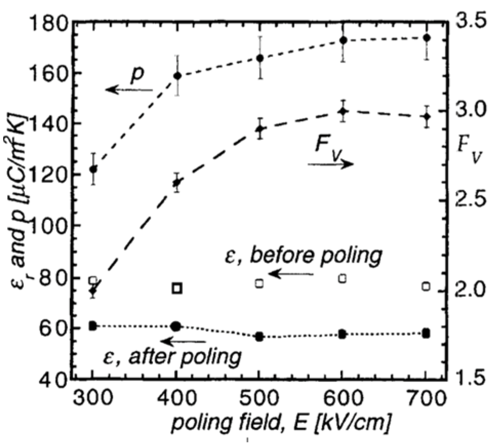
- The relative permittivity of the films increases 148 to 356,
- The dissipation factor increases from 2.5 to 2.84,
- At , the pyroelectric coefficient increases from to ,
- The coercive field decreases from for thin films to for ,
- The remnant polarization decreases from for to for thin films, and
- thin film showed highest values for the figure of merit for voltage and the figure of merit for detectivity .
The data suggest that the thin film is a good candidate for pyroelectric infrared (PIR) sensors. PIR sensors made of this material revealed that the voltage response and the specific detectivity increased with the and this trend continued up to 3 mole %, Ca content, above which the voltage response and specific detectivity degraded.
2.8.2. The Effect of Interfacial Diffusion across the Film Interfaces
Chi et al. [89] reported on the growth of a highly (100)-oriented multilayer film on a substrate at a temperature as low as . This technique takes advantage of the low temperature crystallization and high orientation capabilities of thin films of , which minimizes the interfacial diffusion across boundaries of the multilayer film. These films are advantageous for applications in high figure-of-merit pyroelectric thin-film devices. This is because they simultaneously possess a relatively low dielectric constant and a high pyroelectric coefficient.
2.8.3. The Effect of Contacts
Contacts to a PZT sensor may affect its electrical performance through:
- The choice of contact composition.
- The modification of the contact’s Schottky barrier height (if a blocking contact is formed).
The Choice of Contact Composition
Initially, platinum was used as both top and bottom contact for the devices because of the following advantages:
- is a non-reactive metal and hence suppresses formation of interfacial oxide with the oxygen containing during high temperature steps of the fabrication processes.
- The lattice spacing in the (111) Pt closely matches the (001) plane of , and as a bottom electrode, it acts as a favorable growth template yielding highly textured [001] , with the P directed normal to the electrode surfaces [90].
However, the growth of on produces high angle grain boundaries that cause aging and fatigue due to charge segregation and defect accumulation and amount to long-term device performance reliability issues [91]. Also, oxygen vacancies in create several issues to pyroelectric detectors utilizing such sensing elements, which are initiated by the volatilization of molecules since this induces both and vacancies. For 43:57 compositions, and vacancies constitute the majority of defects and dominate the conduction mechanism up to [92,93]. Hence, the oxygen-permeable electrodes such as [94], [95], [26] were substituted with the top electrode material to reduce the concentration of oxygen vacancies in the material by allowing the reintroduction of oxygen in to the lattice during the post-annealing in the oxygen step. Unlike Pt electrodes, these materials allow for oxygen penetration into the oxide during the electrode annealing step, which reduces oxygen vacancies. Among these oxygen-permeable materials, iridium oxide has attracted much attention due to its thermal stability, reliable performance, relatively high conductivity, and high charge injection capabilities. Iridium oxide hardly reacts with Si, even at high temperatures [96], and makes a good barrier against [97] and [96] diffusion. Yet, it is permeable to diffusion, a property that alleviates reliability issues in device [94]. Iridium oxide is preferred over Pt as a top contact for pyroelectric applications. This is because:
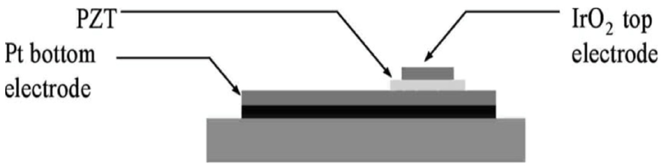
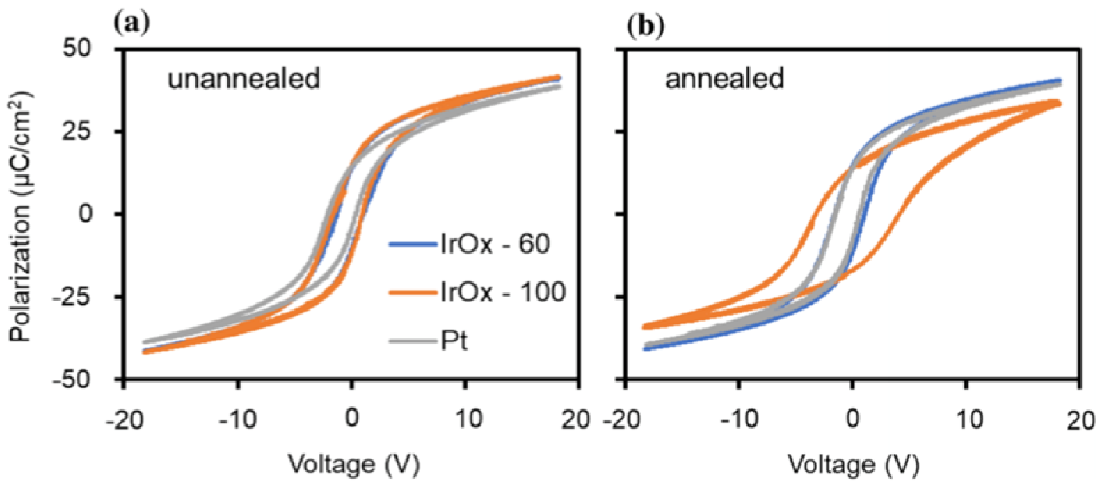
- Iridium oxide has good IR absorption properties, eliminating the need for a separate absorption layer such as electrochemically deposited ‘black’ (with an absorption coefficient of [98]). This design would reduce the effective sensor’s thermal mass and hence provide faster response to the heat compared to [57]. Iridium oxide serves a dual purpose as a top electrode/absorber that provides high polarization of the pyroelectric material, optimizes IR absorption, and minimizes the overall thermal mass.
- Given the same top electrode area, iridium oxide provides a far higher pyroelectric coefficient for films.
- Iridium oxide has a higher dielectric constant and permittivity which translates to a higher pyroelectric responsivity compared to Pt [99,100].
Bouyssou et al. [94] proposed a qualitative and quantitative behavioral model which describes changes in the leakage current of the capacitor as a function of time, voltage, and temperature.
Ohmic versus Blocking Contacts
Blocking contacts present extra impedance to current flow through contact and result in an asymmetric response with respect to the direction of the current. Difficulties may arise for the extreme cases as outlined in Table 3.
Table 3.
Difficulties arising from the blocking contacts.
Since pyroelectric currents are so small, non-ohmic contact may give a symmetric appearance to characteristics. This effect is of primary concern when p is being measured rather than when the performance of a practical device is being assessed.
The Choice of Electrode Layout
When a polarization vector has a component parallel to the surface, interdigitated fingers (Figure 36) are sometimes used on the top surface of the pyroelectric sensor to enhance current capability of the electrode. However, for the measurement of the pyroelectric constant of a material, such configurations are not the geometry of choice since much of the charge that is collected from electrodes incorporate dipoles due to the fringing field located well below the surface, thereby complicating the device analysis [62].
Figure 36.
The layout for interdigitated fingers metallization adapted from [103]. Reprinted from [103], Figure 6, with permission from IEEE.
Transient current characteristics depicted in Figure 37 follow the Curie-Von Schweidler law for , showing the relaxation behavior expected for FE-PZT thin films [94].
Figure 37.
(a) Hysteresis loops of capacitor devices before annealing and (b) after post-top electrode etch annealing in an environment at for 30 min. -60, -100, and Pt electrodes have thicknesses of 100 nm, 700 nm, and 100 nm, respectively [100]. Reproduced from [100], Figure 9, with permission from Springer Nature.
Hanrahan et al. [25] reported on the improvement of the leakage current, remnant polarization, and pyroelectric response of PZT thin film capacitors through the use of the top electrode. The hysteresis loops shown in Figure 37a for the unannealed capacitor seem nearly identical, with a minor increase in the maximum and remnant polarizations for the platelet -100 specimen in Figure 35. Imprint is attributed to a passive layer within the film. Figure 37b reveals that the coercive voltage increases by and maximum remnant polarization decreases in the plate-like structured -100. This is ascribed to an additional low-permittivity dielectric layer arranged in series with the bulk of the PZT film [100].
A transition takes place between , where the measured current increases and an initial current rise is observed at higher temperatures, indicating that a mechanism with relatively slow kinetics is in action. The leakage current in the thin film capacitors above is dominated by the oxygen vacancy hopping. The sample had a Pt top electrode and the pyroelectric film consisted of a excess Pb seed layer and a excess thin film [25]. Figure 38 depicts the results when the bias voltage was switched between measurements. The data confirm the presence of a static Schottky interface at the bottom electrode. The difference in conductance is attributed to a measurement related artifact. Each high temperature test was performed on a fresh sample with supposedly uniform distribution of ionic species distributed through the thickness of the . At the end of the positive voltage cycle, a large concentration gradient of ionic species was established within the sample. The ionic species were electrically biased and thermally activated to drift through the thickness of the sample, during the initial testing cycle. As soon as the negative bias cycle begins, the asymmetrical distribution of ions screens the applied voltage and limits the conduction in this direction.
Leakage current in the thin film capacitors above is dominated by the oxygen vacancy hopping.
Either Schottky emission, Poole-Frenkel emission, or a combination of these two dominates conduction [26,27].
This study supports the assumption that at high temperatures, conduction primarily dominates leakage current with a secondary effect comprising the emission of electrons at one electrode, detected through the asymmetry in current density as shown in Figure 39.
3. Future Trends
The future of pyroelectric materials holds exciting prospects, with several emerging trends shaping the field. Researchers are increasingly exploring the development of multifunctional pyroelectric materials, integrating properties like ferroelectricity and piezoelectricity for versatile applications [104]. Nanotechnology is playing a pivotal role, with a focus on nanostructured pyroelectric materials that exhibit enhanced properties, paving the way for miniaturized devices and improved sensitivity [105]. The trajectory includes a move towards flexible and wearable pyroelectric devices, offering potential applications in health monitoring and energy harvesting from body heat [106]. Efforts are directed towards enhancing the efficiency of pyroelectric energy harvesting, with optimized materials and device designs [107]. The future may witness the evolution of smart and adaptive pyroelectric devices capable of dynamically responding to temperature changes for more versatile functionalities as pyroelectric sensors find utility in smart buildings, environmental monitoring, and energy management systems [108]. Advancements in characterization techniques and a focus on environmental and biomedical applications further highlight the diverse and promising future of pyroelectric materials [104].
Author Contributions
Conceptualization, M.R. and M.F.; methodology, M.R. and M.F.; validation, M.R., M.F. and Y.X.; formal analysis, M.F.; investigation, M.F.; resources, M.F.; writing—original draft preparation, M.F.; writing—review and editing, M.R., M.F. and Y.X; visualization, M.R. and M.F.; supervision, M.R.; project administration, M.R.; funding acquisition, M.R. All authors have read and agreed to the published version of the manuscript.
Funding
This research was funded by the Air Force Office of Scientific Research—grant number FA9550-21-1-0460, FA9550-22-1-0534, the National Science Foundation—award number CNS-2235366 and the Office of Naval Research—grant number N00014-23-1-2742.
Institutional Review Board Statement
Not applicable.
Informed Consent Statement
Not applicable.
Data Availability Statement
No new data had been created as part of this study.
Conflicts of Interest
The authors declare no conflicts of interest.
Appendix A
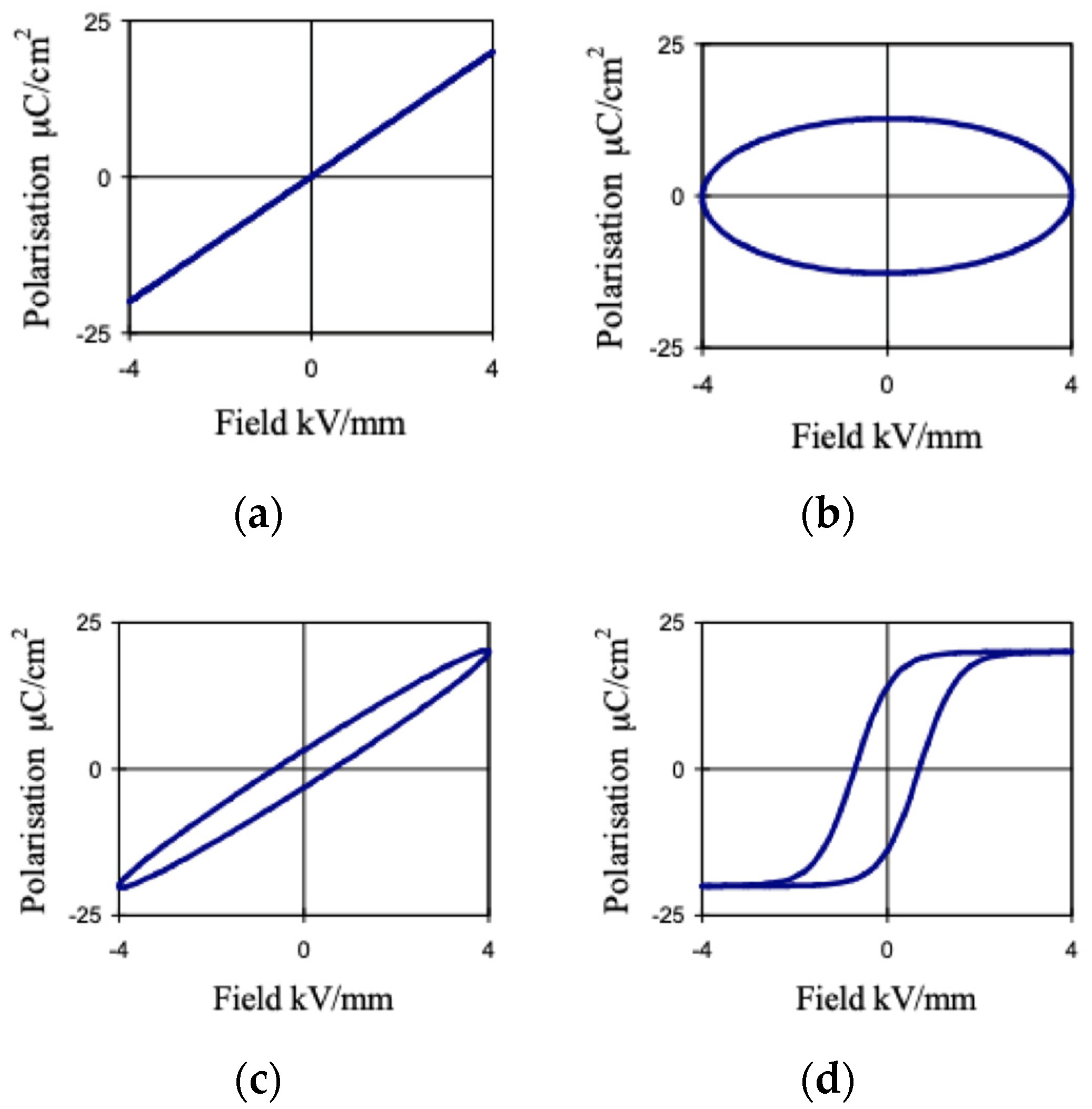
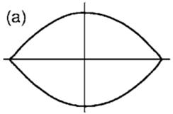
Appendix A.1. P(E) Loops: Development, Artifacts, and Measurement
For an ideal (linear) parallel-plate capacitor with FE insulator, the charge is linearly proportional to voltage (or field) as shown in Figure A1a. The P(E) loop is then a straight line passing through the origin, whose gradient is proportional to capacitance.
Figure A1.
The P(E) loop for (a) an ideal linear capacitor, (b) an ideal resistor, (c) lossy capacitor, and (d) a non-linear lossy capacitor [109]. This figure is reprinted with permission from the journal.
The charge is given by:
where is the remnant polarization and is the electrode area. For an ideal resistor, where the current and voltage are in phase, the loop is generally an ellipse whose center rests at the origin (Figure A1b). If the electrical conductivity of the linear dielectric resistor is , the charge in transit is given by:
where is the measurement time. At fields below which switching occurs, ferroelectric material acts as a lossy linear dielectric and may be modeled by an equivalent resistor representing the dielectric loss in parallel with an ideal capacitor . Thus, the current supplied to this parallel RC network is:
Conceptually, the appearance of the loop for a linear lossy capacitor may be visualized by combining the above two components in parallel, as shown in Figure A1c. Here, the slope is proportional to the capacitance, but the area inside the loop is proportional to the loss tangent of the device. If the electrical conductivity of the linear dielectric is , and the applied electric field is , then:
For a non-linear dielectric such as that of a ferroelectric material where charges saturate at high electric field, a loop is produced, such as that shown in Figure A1d.
Several artifacts may arise during the measurement of loops. Some originate from measurement equipment, while others result due to the sample’s leakage current. A few examples are given in Table A1.
Table A1.
Examples of sources for artifacts which may appear as hysteresis [110]. Reprinted from [110], with permission from the American Physical Society.
Table A1.
Examples of sources for artifacts which may appear as hysteresis [110]. Reprinted from [110], with permission from the American Physical Society.
| Appearance of the Hysteresis Curve | Description |
|---|---|
![]() | Dead short in a Sawyer-Tower bridge type measurement. This kind of result is obtained when the conductivity of the dielectric under test is high. |
![]() | Linear lossy dielectric. The points where the loop crosses are often misinterpreted as values. The elliptical shape is achieved because of the phase shift caused by the dielectric loss. |
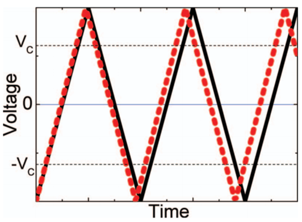
![]() | Saturation of the amplifier in the measurement system leads to an apparently perfectly square hysteresis loop, particularly when the conductivity in (5) is large. When dipole reversal saturates, should not change with in a true hysteresis curve. |
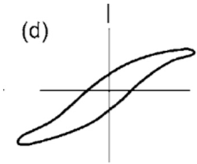
![]() | resembles a real hysteresis curve for a nonlinear lossy dielectric even if it is phase-compensated. One can verify whether it is real or an artifact only by varying the measuring frequency. Artifacts due to dielectric loss are apt to be highly frequency dependent [111]. |
To construct P(E) loops, it is necessary to select a set of data representing a single cycle of the electric field waveform [112]. The data corresponding to the start and end points of the loop are identified by detecting when the electric field waveform crosses the horizontal time axis with either a positive or negative slope. The charge stored in the device under test (DUT) at any given time is calculated via numerical integration of the current :
Assuming that specimen area is , the dielectric displacement is calculated as:
For high permittivity ferroelectrics, . However, for low permittivity dielectrics, a small correction is needed. Then, is calculated from [112]:
Appendix A.2. Measurement of the Dielectric Permittivity
It is given by , where is the polarization density. Because under the static condition inside the conductor, for a metal, . For a lossy dielectric, relative dielectric constant is a complex number with two components: one in phase, and the other out of phase, . It is represented as . Upon the application of a voltage to such a dielectric, most of the absorbed energy is lost to heat. Dissipation factor () or loss tangent is defined as the inverse ratio of the dielectric’s capacitive reactance to its equivalent series resistance, or the ratio between the permittivity and the conductivity of an insulator at a specified frequency. is a dimensionless quantity that indicates how much energy a material loses to heat. For an ideal insulator, . The ratio is called power factor.
Debye’s relaxation model characterizes the dynamic polarization response of an ideal, noninteracting population of dipoles with only one relaxation time to an alternating external electric field. Assuming and are the low (static) and high frequency limits of the permittivity, respectively, it is expressed in the complex permittivity of a medium as a function of the angular frequency of the electric field as:
where and is the characteristic relaxation time of the medium. The real and imaginary parts of the complex dielectric permittivity are given by (A9) and (A10) respectively:
The dielectric loss (loss tangent) is given by:
To measure , a small signal superimposed upon a bias is applied to the sample, and an impedance analyzer is used to measure the real and imaginary parts of the impedance. By doing so, the impedance analyzer balances sample impedance with a set of internal reference impedances. There are now commercial systems that automatically measure both the capacitance and loss tangent.
Appendix A.3. Transport Mechanisms in Thin Films
A knowledge of conduction mechanisms in the dielectric films is indispensable since it helps to identify device failure mechanisms and allows for the minimization of the undesirable leakage current. Transport characteristics in thin dielectric films may be traced either to the contact (contact-limited) or to the bulk (bulk-limited) properties of the dielectric. In practice, depending on the specific experimental conditions (applied field, temperature, illumination density, etc.), one or more of the mechanisms discussed below may govern the overall characteristics. The methods for distinguishing between these mechanisms rely on how conductivity is influenced by temperature and/or the applied voltage [113].
Appendix A.3.1. Contact-Limited Conduction Mechanisms
If a blocking contact exists at a metal-dielectric interface, the conduction process is said to be electrode-limited and ordinarily, it will not become bulk-limited with increasing applied voltage unless the dielectric is thick.
Figure A2 schematically shows the three mechanisms an electron may use to pass through a barrier. These are: (i) surmounting the barrier by thermionic (Schottky) emission, (ii) passing through the barrier (Fowler-Nordheim tunneling), and (iii) a thermal excitation followed by a tunneling through a narrow triangular barrier (thermionic-field emission).
Figure A2.
Classification of the three electrode limited leakage mechanisms in insulators: thermionic emission, thermionic-field emission, and Fowler–Nordheim tunneling. Reproduced from [114], Figure 1 (CC BY-NC 3.0).
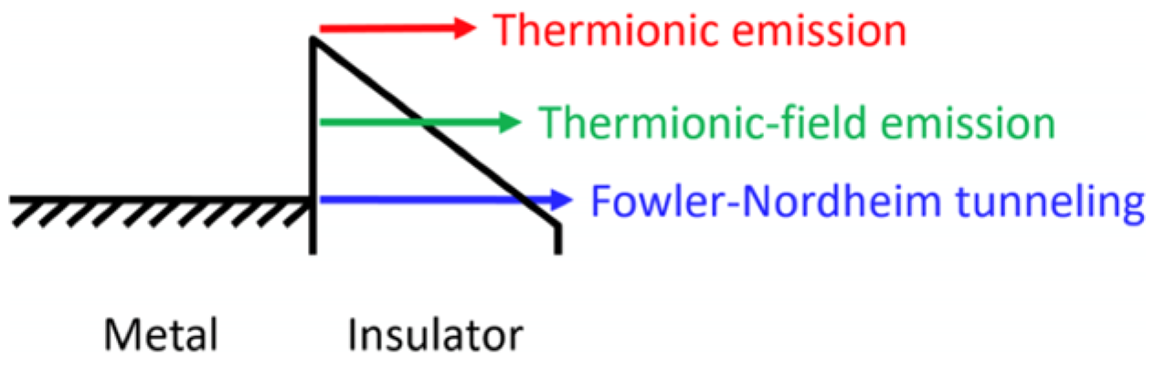
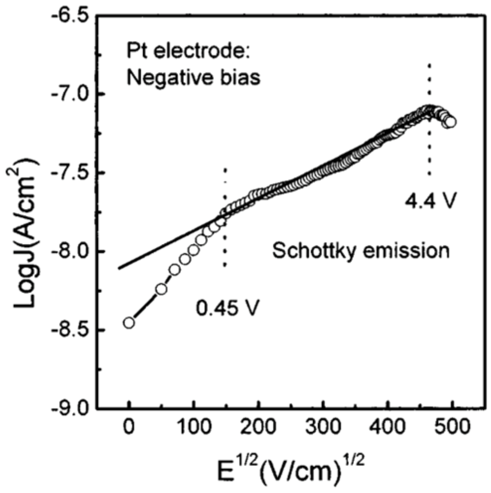
Thermionic (Schottky) Emission
Thermionic emission is the prevalent transport mechanism in perovskites and metal insulator interfaces, especially at relatively high temperatures. It describes a conduction process initiated by thermally activated electrons that are injected over an energy barrier into the conduction band of the perovskite/oxide. Then, by providing sufficient energy, an externally applied field can enable more electrons (compared to equilibrium) to confront the barrier and encourage them to overcome the barrier The conduction is thus limited by the emission of electrons over the barrier. The current density is given by:
where is the effective Richardson constant, is the elementary charge, is the electron effective mass in the dielectric insulator, is Boltzmann’s constant, is the electronic charge, is the absolute temperature, is Planck’s constant, is electric field at the interface (or across the oxide), is carrier mobility, is the barrier height (i.e., conduction band offset), and , where is the vacuum permittivity and is the optical dielectric constant. The optical dielectric constant, rather than the static dielectric constant, is used because the dielectric constant is a function of frequency. During the emission process, if the electron jump period from the metal’s Fermi level at the interface to the barrier top is shorter than the dielectric relaxation time, the dielectric will not have enough time to be polarized. Consequently, the proper choice for is the optical (high frequency) dielectric constant [115,116], which is smaller than the static (low frequency) dielectric constant, where more polarization mechanisms contribute to the total polarization [117]. The dynamic dielectric constant , where is the insulator’s refractive index and is thus generally a function of frequency.
The characteristic is asymmetric with respect to positive and negative voltages. Although the Schottky equation is widely used to describe the conduction in perovskite-type titanate films, it generally yields inconsistent values for and . Zafar et al. [41] resolved this issue by modifying the standard Schottky equation. Furthermore, they showed that at lower frequencies, charge injection in , a substance which has proved to be effective as contact for most perovskites’ films, can be adequately described by the Schottky expression, while at higher fields, unified thermionic and field emission of the approach proposed by Murphy and Good [118] is more consistent.
When an electron departs metal, it leaves behind a positive ion. This process leads to the effective reduction of the Schottky barrier height (called image-force-induced Schottky barrier lowering) by an amount given by [23]:
Since the tunneling exponentially depends on the barrier height, image-force barrier lowering effectively increases the insulator’s tunneling current. From Equation (A13), it follows that:
Thus, if the Schottky injection is the dominant mechanism for the carrier transport, a plot of versus is linear with a slope of .
Thermionic-Field Emission
Figure A4 depicts a schematic of the energy band diagram for the thermionic-field emission, where electrons having an energy between the metal’s Fermi energy (capable of field emission) and the dielectric’s conduction band edge (capable of Schottky emission) tunnel through the triangular barrier. The current density due to thermionic-field emission can be roughly expressed as [7]:
Fowler-Nordheim (F-N) Tunneling
Figure A5a depicts the schematic energy band diagram of F-N tunneling. When the insulator thickness is less than , electron wave function may penetrate through the potential barrier. The electron tunneling probability depends not only on the thickness, but also on the height, width, and the structure of the barrier, as well as the applied electric field.
The expression of the F-N tunneling current is:
where is the electron’s tunneling effective mass in the dielectric. The other notations in the equation above have already been described earlier. Experimental results conform with theory, particularly at higher electric fields. A plot of versus ( plot) is linear, with a slope , which is a function of both electron effective mass and barrier height:
Despite the fact that tunneling through thick insulators (>50 A°) is highly unlikely, Stolichnov et al. [44] reports on detection of entirely direct tunneling currents in a thick films at temperatures between and . Their observation could be explained if it is assumed that shallow traps existed in the insulator band gap. In this case, an electron may tunnel into a trap level and is then transported through the insulator via hopping conduction, as shown in Figure A5b. Then, the barrier height obtained using Equation (A17) will give the energy position of traps in the dielectric band gap with respect to the metal’s Fermi level. Nevertheless, the range of data on the electric field (from to ) is too limited to unambiguously identify the current mechanism.
Since the tunneling probabilities depend on the shape of the tunneling barrier, different probabilities (and hence currents) are obtained for the , where the barrier is triangular, and for the direct tunneling, where the barrier is trapezoidal.
In general, if insulator thickness is wide enough, the tunneling effective mass can be assumed to be equal to the electron effective mass for dielectric films. To extract and , it is useful to measure the at a high temperature where thermionic emission dominates and at a low temperature where the tunneling current dominates [113]. Using a mathematical iteration method, the electron effective mass in the insulator and barrier height at the interface can then be determined using the intercept of Schottky plot at high temperatures and the slope of plot at low temperatures.
Appendix A.3.2. Bulk-Limited Conduction Mechanisms
These mechanisms solely depend on the electrical properties of the bulk dielectric insulator such as the trap distribution and energy level and comprise (1) Poole-Frenkel emission, (2) hopping conduction, (3) ohmic conduction, (4) space charge-limited conduction, (5) ionic conduction, and (6) grain-boundary-limited conduction. The study of the bulk-limited conduction mechanisms can reveal some of the important electrical properties in the dielectric films, including the trap energy level, spacing, and density as well as the carrier drift mobility, the dielectric relaxation time, and the density of states in the dielectric conduction band.
Poole-Frenkel (P-F)
Poole-Frenkel emission involves the thermal excitation of electrons from bulk traps (e.g., oxygen vacancies) into the dielectric conduction band. Assuming that Coulomb interaction exists between electrons and traps, the potential energy of a trapped electron is then reduced when an electric field is applied across the dielectric and the probability that a trapped electron is thermally emitted into the conduction band of the insulator is increased, as schematically depicted in Figure A6.
Figure A6.
Schematic energy band diagram of Poole-Frenkel emission in MIM structure [120]. Reproduced from [120], with permission from MDPI.
In contrast to Schottky emission, for P-F conduction mechanism, the I-V characteristic is symmetric with respect to positive and negative voltages [45].
The current density due to the P-F emission is given by:
where is the electron drift mobility, NC is the density of states in the dielectric conduction band, and is the trap energy level. The other relevant notations were defined earlier. The P-F mechanism relies on thermal activation and externally applied electric field and thus dominates under such circumstances. The trap energy level can be extracted experimentally from the Arrhenius plot of versus (P-F plot). The trap barrier height is extracted from the intercept of P-F plot.
The distinction between the Schottky and PF mechanisms is sometimes challenging. This is because, from Equations (A12) and (A16), it follows that:
where and represent the slopes of and versus , respectively. Considering Equations (A19) and (A20), both the Schottky and PF models may fit fairly well with experimental data irrespective of the dielectric thickness. To distinguish between the two mechanisms, Chantier et al. [27] proposed extracting the refractive index as follows:
where represents either the Schottky or PF mechanism. Then, the comparison between the theoretical values reported in the literature with the experimental data reveals the dominant current mechanism. As a final means to distinguish between the Schottky emission and P-F mechanism, the effect of electrode material on the conduction characteristics can be examined.
Hopping Conduction
A trapped electron may initiate a conduction by tunneling into its nearest neighbor trap site. This process is referred to as nearest neighbor hopping (NNH). The current density is given by:
where is the electrical conductivity at . A second hopping conduction mechanism known as Mott variable range hopping (VRH) is observed in strongly disordered systems with localized charge-carrier states, where the electron is likely to hop into a trap that is further away but has lower trap energy. The energy band diagram of Figure A7 describes both the NNH and VRH processes [120].
Figure A7.
Schematic energy band diagram of Nearest Neighbor Hopping (NNH) and Variable-range Hopping (VRH) model in an MIM structure [120]. Reproduced from [120], with permission from MDPI.
In the P-F emission, carriers need to overcome the trap barrier through a thermionic mechanism, while the hopping conduction relies on a tunneling effect. In hopping conduction, the carrier energy is lower than the maximum energy of the potential barrier between the two trapping sites, but the carriers can still transit using the tunneling mechanism.
Simulation of hopping conduction allows for determining the range of electric field and temperatures for which hopping conduction becomes dominant. Using the slopes of the Arrhenius plot in low fields, the activation energy is extracted. Defects with deeper energy levels are activated at higher temperatures. This leads to an exponential decrease in . For Mott VRH transport, the current density is given by [120]:
where is the electrical conductivity at . Similar to Ohmic conduction, is proportional to the applied electric field. Nevertheless, the conductance obeys temperature dependency given by .
Trap-Assisted Tunneling (TAT)
This is another possible hopping mechanism attributed to the tunneling current which is assisted by the defects in the dielectric. Unlike F-N or direct single-step tunneling, the traps in dielectric assist the electrons to tunnel from cathode to anode through a 2-step process by first capturing electrons from the cathode and subsequently emitting it to the anode. For inelastic TAT, the electron will relax to the trap’s energy level by emitting one or more phonons. The expression for the TAT current density is [120]:
where is a constant and is the energy of the electron traps with respect to the conduction band edge of the dielectric.
Ohmic Conduction
Figure A8 shows a schematic energy band diagram for the Ohmic conduction. Even for dielectrics with large band gaps, electrons from valance band or from the impurity levels within the energy gap may still become thermally excited.
Figure A8.
A typical current density-voltage characteristic of space-charge-limited conduction current. is called the transition voltage. is the trap-filled limit voltage [113]. “Copyright © 2014 Chiu, F.C. A review on conduction mechanisms in dielectric films. Advances in Materials Science and Engineering, 2014, 2014, pp. 1–18, Figure 24, Figure 28 and Figure 30. https://doi.org/10.1155/2014/578168. This is an open access article distributed under the Creative Commons Attribution License, which permits unrestricted use, distribution, and reproduction in any medium”.
Ohmic conduction stems from the movement of thermally generated carriers under an applied field and leads to a linear relationship for , expressed as:
where is electrical conductivity, is electron mobility, and is the electric field across the dielectric. The concentration of electrons in the conduction band is given by:
Here, is the effective density of states in the conduction band; the other terms are as defined above. Because the carrier concentration is negligible, and . Hence,
This current component is very small in magnitude and is observed at very low voltages in characteristics of the dielectric films [113].
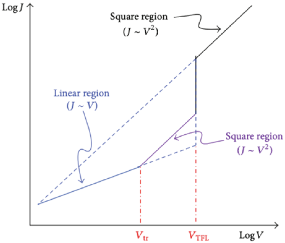
Space-Charge-Limited Current (SCLC)
When charges are injected through ohmic contacts in an insulator with traps distributed throughout its band gap, a large fraction of the charges may become trapped in the insulator. These trapped charges reduce the magnitude of the SCLCs and modify the shape of the from an ideal square law to a higher power dependence on voltage. Furthermore, since the occupancy of a trap is a strong function of temperature, SCLC will have a temperature dependence that depends on the trap energy. In practice, the SCLCs are less than their theoretical value for an ideal crystal by the ratio of free to trapped carriers. Therefore, the SCLCs may be utilized as a simple tool for measuring the imperfections in crystals, even in the range of one part in .
As depicted in Figure A8, a typical characteristic for space-charge-limited current plotted in a log-log format is bound by the three limiting curves: (i) ohm’s law , (ii) traps-filled limit , and (iii) the Child’s law . and mark the transition voltages at the boundary between ohm’s law and TFL curve, respectively [121]:
where is the concentration of the free charge carriers in thermal equilibrium, is the applied voltage, is the thickness of thin films, is the static dielectric constant dielectric constant, and is the quantity defined in Equation (A32). The transit and the dielectric relaxation time are denoted by and , respectively.
Table A2 gives further details for carriers’ distribution in dielectric film under carriers’ weak injection under space-charge-limited conduction.
Table A2.
Carriers’ distribution in dielectric film under carriers’ weak injection [113]. Reproduced from Chiu et al. [113], an open access article distributed under the Creative Commons Attribution License, which permits “unrestricted use, distribution, and reproduction in any medium”.
Table A2.
Carriers’ distribution in dielectric film under carriers’ weak injection [113]. Reproduced from Chiu et al. [113], an open access article distributed under the Creative Commons Attribution License, which permits “unrestricted use, distribution, and reproduction in any medium”.
| Regime | Conditions | Characteristics | Schematic of the Physical Process |
|---|---|---|---|
| Very weak injection | : slow | Space charge exists next to the contact. | ![]() |
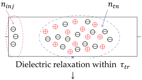
| Dielectric relaxation | , thus . For charge neutrality and injected carriers. Redistributed relaxed in a time | The injected carriers cannot travel across the insulator. | ![]() |
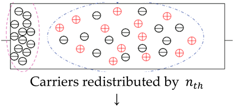
| Weak injection | , , Traps are partially filled. | , marks border between the ohmic and SCLC (1st square law) regimes. | ![]() |
Table A3 gives details for carrier distribution in dielectric films under strong injection and in space-charge-limited conduction .
Table A3.
Carriers’ distribution in dielectric film: the case of strong injection, where the traps are filled up and a space charge appears [113]. Reproduced from Chiu et al. [113], an open access article distributed under the Creative Commons Attribution License, which permits “unrestricted use, distribution, and reproduction in any medium”.
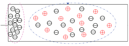
| Regime | Conditions | Conclusion | Schematic of the Physical Process |
|---|---|---|---|
| Onset of square law: , , is too short for charges due to to be relaxed by those due to | , , both and decrease as is increased. , traps remain empty, and dielectric is not relaxed. | Injected carriers transit the device without noticing the traps. applies. | ![]() |
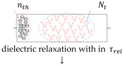
| Trap-limited: , while reaches , the traps are progressively filled. | For , as increases, also increases. Thus moves up in energy but still . Some of the traps are filled with injected carriers. | Trapped-filled limited trapped behavior: dielectric becomes partially relaxed in a time . | ![]() |
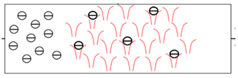
| Trap-free SCLC: once all traps are filled, a space charge builds up for causing a jump in at . | , approaches . Electric field is no longer constant across the dielectric. SCLC limits further injection of free carriers in the dielectric. | The conduction becomes fully space-charge-limited (Child’s law: ), with a jump from a low trap-limited value to a high trap-free SCLC. | ![]() |
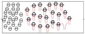
The trap-filled limit (TFL) is the condition for the transition from the trapped characteristics to the trap-free characteristics. is defined as the voltage required to fill the traps, i.e., it is the voltage at which the Fermi level passes through . It is possible that space-charge-limited current dominates when a sample is biased in one direction, whereas for the opposite bias, Schottky injection dominates.
Ionic Conduction
Under high electric fields and temperatures, ions may travel by jumping over potential barriers from one defect site to another in the direction dictated by the applied electric field. Ions with larger masses will have smaller mobilities. In pyroelectric insulators, ion masses are generally large, while and are relatively small; hence, ionic conduction is not very likely.
A schematic energy band diagram is given in Figure A9 for two cases: (a) the absence and (b) the presence of an electric field . The spacing between ionic sites is , and the barrier height potential is .
Figure A9.
Energy band diagram of ionic conduction (a) without an applied electric field and (b) with the applied electric field [113]. Reproduced from Chiu et al. [113], an open access article distributed under the Creative Commons Attribution License, which permits “unrestricted use, distribution, and reproduction in any medium”.
The ionic conduction current can be expressed as:
where is a proportional constant, is the potential barrier height, and is the spacing between two nearby jumping sites; the other symbols have been defined earlier [113].
Grain-Boundary-Limited Conduction
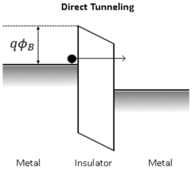
Surface recombination of carriers at the grain boundaries of a polycrystalline material is a function of several parameters, including temperature, grain size, grain orientation, impurity concentration, etc., and is responsible for increased resistivity at the grain boundaries compared to the grain’s bulk. The carriers are scattered by the scattering centers (e.g., charged impurities or defects) residing on the grain boundaries when they are transported from one grain to the next. This mechanism may dominate the conduction properties of the DUT when the grain size is reduced [9,32].
A second mechanism is attributed to the Schottky effect. A potential barrier energy,
is developed at the grain boundary, where is the grain boundary trap density, is the relative dielectric constant of the polycrystalline material, and is the local dopant concentration. Therefore, energy bands bend at the grain boundaries, allowing only electrons with a thermal energy to cross the barrier (Figure A10). In this case also, the charge transport properties of the polycrystalline film are affected by the electrical properties of the Schottky barrier height at the grain boundaries rather than bulk.
Figure A10.
Schematic energy band diagram for grain-boundary limited conduction in a metal-insulator-metal structure [113]. Reproduced from Chiu et al. [113], an open access article distributed under the Creative Commons Attribution License, which permits “unrestricted use, distribution, and reproduction in any medium”.
Using impedance spectroscopy [102], grain boundary-limited conduction may be differentiated from the bulk contribution in total conductivity on the account of different relaxation times associated with their response to an AC signal [113].
Direct Tunneling
The direct tunneling current component dominates when insulator thickness becomes very thin (<4 nm). In this case, electrons residing on the metal’s Fermi level face the energy barrier of the full oxide thickness. Electrons then will have to tunnel through the trapezoidal potential barrier instead of tunneling through a triangular potential barrier, as was the case for the FN tunneling. The direct tunneling occurs at .
Figure A11.
Direct tunneling of electrons [120]. Reproduced from [120], with permission from MDPI.
The equation governing the current density of the direct tunneling is given by [119]:
Contreras et al. [122] reported on the production of metal-PZT-metal junctions that were sufficiently thin (< 6 nm) for electrons to tunnel through the FE insulator, either directly or through a phonon-assisted process. However, a value much smaller than expected was obtained for the barrier height.
Transition from Electrode-Limited to Bulk-Limited Conduction Processes
For highly doped and/or defective insulating film, the conduction process may vary from being electrode-limited at low voltages with essentially thickness-independent and very steep characteristics to being bulk-limited at high voltages where the current rises less rapidly with increasing voltage, and there is a linear relationship between and . The slope of this curve depends on the nature of the defective structure of the insulator [47]. PT-based insulators generally include donors, traps, and perhaps acceptors that act as compensating centers simultaneously and hence comprise more complicated systems.
Appendix A.3.3. Electrical Breakdown
There are two mechanisms generally held responsible for breakdown in the dielectric materials: ionic conduction and thermal breakdown (thermal runaway).
Ionic Conduction
Under high electric fields, electrons injected from the cathode by field emission multiply in the dielectric material through ionizing collisions. The breakdown process in arises from the growth of ordered chains of oxygen-deficient material and leads to a dendrite-like conduction pathways through the material, which act as “virtual cathodes”. It can be initiated either at the anode and/or at the cathode of the device. The process of electrical breakdown in arise from dendrite-like conduction pathways through the material which may be initiated at the anodes and/or cathodes with a power-law dependence on thickness as:
with , according to the linked defect model by Gerson and Marshall [123]. The dependence on electrode material arises from the work function and the electron affinity of the electrode through the resulting Schottky barrier height. As long as , where is the lattice nearest-neighbor oxygen-site hopping distance (approximately a lattice constant), Scott [115] showed that the relation defined as follows:
may be used to estimate the breakdown field for most ferroelectrics. Using (A39), values of approximately 8 MV/cm are predicted to conform well with measurements. On the basis of the electron-lattice scattering mechanism in dielectric materials and the electron behavior in the conduction band of the dielectric, Forlani and Minnaja [124] derived the ionization avalanche probability and evaluated the current density by assuming that electrons are injected through tunneling at the negatively biased contact. The criteria for the onset of breakdown are relevant when the current density reaches some arbitrary value. This treatment reveals a correlation between breakdown field strengths and dielectric thickness. The results derived are applicable to an estimate of the temperature of electrons injected by a tunnel cathode of the metal-dielectric-metal type.
Thermal Breakdown (Thermal Runaway)
Power dissipation in a device usually generates heat, which in turn leads to a temperature rise in the device. Since the temperature coefficient of the conductivity is positive, a positive feedback scenario may develop where the device temperature increases without bound. This leads to device instability and eventually to thermal runaway. Dependence of FE oxides on temperature is complicated, generally consisting of a hybrid mechanism comprising an initial electrical phase followed by simple thermal runaway.
Appendix A.4. Leakage Current Characterization Protocol
Since the time constant associated with an insulator is large, the transient (relaxation) current is generally one of the key artifacts encountered in the measurement of the leakage current, particularly when the insulator is a defective dielectric. As noted in Equation (A4), in a pulsed measurement system, depends on the pulse width.
Bouyssou, et al. [42], showed that the resistance degradation (RD) mechanism in is a reversible phenomenon.
Figure A12.
characteristics of capacitors biased at 5 V at 140 °C during 600 s, after waiting periods ranging from 0 s to 2400 s [42]. Reversible RD mechanisms occur during the waiting period (i.e., the time during which 0 V is applied to the capacitor). Reprinted from [42], Figure 3, with permission from Elsevier.
Thus, in each measurement step, sufficient time must be allocated to ensure the measurement of leakage current is carried under steady state condition. Based on the transient current data, Chentir et al. [27] established a characterization protocol to minimize the contribution of artifacts to the measurements of leakage current.
A typical representation of the evolution of leakage current for capacitor biased under 5 V at 200 °C is shown in Figure A13. Due to high thermal stress, relaxation and RD occur briefly. After resistance restoration (RR) process is completed, the current remains steady up to 90% of the capacitor’s lifetime.
Figure A13.
Typical evolution of leakage current for a capacitor submitted to a CVS of 5 V at a temperature of 200 °C. At the end of RR, the leakage current remains steady, and it lasts up to 90% of the capacitor lifetime [27]. Reprinted from [27], Figure 5, Figure 7, Figure 8 and Figure 14, with the permission of AIP Publishing.
The leakage current must remain stable during each step of voltage sweep for each temperature. Due to large thermal time constants involved at room temperature, after RR is reached, it may take several weeks to attain steady state. Thus, a pretreatment consisting of applying a constant electric field stress (CES) of 58.33 MV/m at 205 °C is used in order to reach the end of RR state before I(E) measurements, as illustrated in Figure A14. After each prestress, a rather soft CES of about 2 MV/m is kept during temperature sweep to avoid any reversible phenomena.
Once the prestress is accomplished and the test temperature is set, I(E) measurements are performed from 25 MV/m to 83 MV/m at temperatures ranging from 100 °C to 200 °C.
This protocol was applied to determine the influence of thickness on leakage current behavior while excluding perturbations induced by measurement artifacts [38].
Figure A14.
I(t) characteristics of prestressed capacitors before I(E) test. The prestress is performed under a constant electric field of 58.33 MV/m at 205 °C. The prestress is stopped when RR has ended [27]. Reprinted from [27], Figure 5, Figure 7, Figure 8 and Figure 14, with the permission of AIP Publishing.
Hanrahan [25] utilized a Radiant Technologies Precision Premier II FE testing unit in conjunction with a controlled heating probe station. A schematic of the tested structure is shown in Figure A15. This set up was used to measure bipolar current voltage as well as dielectric hysteresis characteristics at frequencies of , with amplitudes of .
The I(V) testing procedure utilized for the assessment of the evolution of the leakage current is depicted in Figure A16. The transient current response at E∼100 MV/m was measured.
Figure A16.
Schematic of a stepwise voltage increase utilized for I–V testing procedure. Samples are exposed to a pulsed voltage equal to the maximum bias to be experienced by the sample during the I(V) characterization. Charge is measured for 100 ms following a 4-s hold after a step voltage increase for all but one test, which used a 10-ms hold and measurement intervals. Voltage is swept from zero to the maximum positive voltage, either 5 or 10 V (10 or 20 MV/m equivalent electric fields), and then reset to zero and measured in the negative direction. For temperatures , the bi-polar bias was reduced from 10 V to 5 V to prevent dielectric breakdown. Temperature was controlled with a resolution of ±5 °C [25]. Reproduced from [25], Figure 4, Figure 5 and Figure 7, with permission from IOP Publishing.
Finally, to eliminate the unwanted contribution of polarization (dielectric relaxation) current, researchers [25,38,84,125] used a long hold time to measure leakage current.
References
- Scott, J.F.; Carlos, A.P. Ferroelectric memories. Science 1989, 246, 1400–1405. [Google Scholar] [CrossRef] [PubMed]
- Pintilie, L.; Lisca, M.; Alexe, M. Polarization reversal and capacitance-voltage characteristic of epitaxial Pb (Zr, Ti) O3 layers. Appl. Phys. Lett. 2005, 86, 192902-2–192903-3. [Google Scholar] [CrossRef]
- Tang, X.G.; Wang, J.; Zhang, Y.W.; Chan, H.L.W. Leakage current and relaxation characteristics of highly (111)-oriented lead calcium titanate thin films. J. Appl. Phys. 2003, 94, 5163–5166. [Google Scholar] [CrossRef]
- Warren, W.L.; Dimos, D.; Waser, R.M. Degradation mechanisms in ferroelectric and high-permittivity perovskites. MRS Bull. 1996, 21, 40–45. [Google Scholar] [CrossRef]
- Ichinose, H.M. Preparation and properties of (Pb,Ca)TiO3 thin films by multiple-cathode sputtering. Jpn. J. Appl. Phys. 1997, 36, 5825. [Google Scholar] [CrossRef]
- Guo, H.Y.; Xu, J.B.; Wilson, I.H.; Xie, Z.; Luo, E.Z. Study of microscopic piezoelectricity of (Pb0.76Ca0.24) TiO3 thin films. Phys. Lett. A 2002, 294, 217–221. [Google Scholar] [CrossRef]
- Liu, F.; Fina, I.; Bertacco, R.; Fontcuberta, J. Unravelling and controlling hidden imprint fields in ferroelectric capacitors. Sci. Rep. 2016, 6, 25028. [Google Scholar] [CrossRef]
- Lo, V.C.; Chen, Z.J. Simulation of the effects of space charge and Schottky barriers on ferroelectric thin film capacitor using Landau Khalatnikov theory. IEEE Trans. Ultrason. Ferroelectr. Freq. Control 2002, 49, 980–986. [Google Scholar] [CrossRef]
- Tagantsev, A.K.; Stolichnov, I.; Setter, N.; Cross, J.S. Nature of nonlinear imprint in ferroelectric films and long-term prediction of polarization loss in ferroelectric memories. J. Appl. Phys. 2004, 96, 6616–6623. [Google Scholar] [CrossRef]
- Pandya, S.; Wilbur, J.; Kim, J.; Gao, R.; Dasgupta, A.; Dames, C.; Martin, L.W. Pyroelectric energy conversion with large energy and power density in relaxor ferroelectric thin films. Nat. Mater. 2018, 17, 432–438. [Google Scholar] [CrossRef]
- Sidorkin, S.; Nesterenko, L.P.; Bocharova, I.A.; Smirnov, G.L.; Sidorkin, V.A.; Ryabtsev, S.V.; Smirnov, A.L. Dispersion of dielectric permittivity in thin ferroelectric lead titanate films. Solid State Phenom. 2006, 115, 236–237. [Google Scholar] [CrossRef]
- Shaw, T.M.; Trolier-McKinstry, S.; McIntyre, P.C. The properties of ferroelectric films at small dimensions. Annu. Rev. Mater. Sci. 2000, 30, 263–298. [Google Scholar] [CrossRef]
- Dahl, Ø.; Grepstad, J.K.; Tybell, T. Crystalline and dielectric properties of sputter deposited PbTiO3 thin films. J. Appl. Phys. 2008, 103. [Google Scholar] [CrossRef]
- Ku, H.Y.; Ullman, F.G. Capacitance of thin dielectric structures. J. Appl. Phys. 1964, 35, 265–267. [Google Scholar] [CrossRef]
- Okuyama, M.; Matsui, Y.; Nakano, H.; Nakagawa, T.; Hamakawa, Y. Preparation of PbTiO3 ferroelectric thin film by RF sputtering. Jpn. J. Appl. Phys. 1979, 18, 1633–1634. [Google Scholar] [CrossRef]
- Larsen, P.K.; Dormans, G.J.M.; Taylor, D.J.; Van Veldhoven, P.J. Ferroelectric properties and fatigue of PbZr0.51Ti0.49O3 thin films of varying thickness: Blocking layer model. J. Appl. Phys. 1994, 76, 2405–2413. [Google Scholar] [CrossRef]
- Fujisawa, H.; Nakashima, S.; Kaibara, K.; Shimizu, M.; Niu, H. Size effects of epitaxial and polycrystalline Pb (Zr, Ti) O3 thin films grown by metalorganic chemical vapor deposition. Jpn. J. Appl. Phys. 1999, 38, 5392–5396. [Google Scholar] [CrossRef]
- Pintilie, L.; Vrejoiu, I.; Hesse, D.; LeRhun, G.; Alexe, M. Extrinsic contributions to the apparent thickness dependence of the dielectric constant in epitaxial Pb (Zr, Ti) O3 thin films. Phys. Rev. B 2007, 75, 224113. [Google Scholar] [CrossRef]
- Bolten, D.; Böttger, U.; Waser, R. Reversible and irreversible polarization processes in ferroelectric ceramics and thin films. J. Appl. Phys. 2003, 93, 1735–1742. [Google Scholar] [CrossRef]
- Basceri, C.; Streiffer, S.K.; Kingon, A.I.; Waser, R. The dielectric response as a function of temperature and film thickness of fiber-textured (Ba, Sr)TiO3 thin films grown by chemical vapor deposition. J. Appl. Phys. 1997, 82, 2497–2504. [Google Scholar] [CrossRef]
- Outzourhit, A.; Naziripour, A.; Trefny, J.U.; Kito, T.; Yarar, B.; Yandrofski, R.; Cuchiaro, J.D.; Hermann, A.M. A comparative study of tunable Ba1−xSrxTiO3 thin film capacitors prepared by rf-sputtering and liquid-phase deposition. Integr. Ferroelectr. 1995, 9, 227–241. [Google Scholar] [CrossRef]
- Wouters, D.J.; Willems, G.J.; Maes, H.E. Electrical conductivity in ferroelectric thin films. Microelectron. Eng. 1995, 29, 249–256. [Google Scholar] [CrossRef]
- Sze, S.M.; Li, Y.; Ng, K.K. Physics of Semiconductor Devices, 3rd ed.; Walker, J., Ed.; Wiley-Interscience: Hoboken, NJ, USA, 2007. [Google Scholar]
- Dixit, A.V.; Rajopadhye, N.R.; Bhoraskar, S.V. Secondary electron emission of doped PZT ceramics. J. Mater. Sci. 1986, 21, 2798–2802. [Google Scholar] [CrossRef]
- Hanrahan, B.; Sanchez, L.; Waits, C.M.; Polcawich, R.G. Improved pyroelectric performance for thin film lead zirconate titanate (PZT) capacitors with IrO2 electrodes. Smart Mater. Struct. 2016, 25, 015025. [Google Scholar] [CrossRef]
- Nagaraj, B.; Aggarwal, S.; Song, T.K.; Sawhney, T.; Ramesh, R. Leakage current mechanisms in lead-based thin-film ferroelectric capacitors. Phys. Rev. B 1999, 59, 16022–16027. [Google Scholar] [CrossRef]
- Chentir, M.T.; Bouyssou, E.; Ventura, L.; Anceau, C. Leakage current evolution versus dielectric thickness in lead zirconate titanate thin film capacitors. J. Appl. Phys. 2009, 105, 061605. [Google Scholar] [CrossRef]
- Lau, W.S. An extended unified Schottky-Poole-Frenkel theory to explain the current-voltage characteristics of thin film metal-insulator-metal capacitors with examples for various high-k dielectric materials. ECS J. Solid State Sci. Technol. 2012, 1, N139–N148. [Google Scholar] [CrossRef]
- Mihara, T.; Watanabe, H.W.H. Electronic Conduction Characteristics of Sel-Gel Ferroelectric Pb (Zr0.4Ti0.6) O3 Thin-Film Capacitors: Part II. Jpn. J. Appl. Phys. 1995, 34, 5674–5682. [Google Scholar] [CrossRef]
- Sudhama, C.; Campbell, A.C.; Maniar, P.D.; Jones, R.E.; Moazzami, R.; Mogab, C.J.; Lee, J.C. A model for electrical conduction in metal-ferroelectric-metal thin-film capacitors. J. Appl. Phys. 1994, 75, 1014–1022. [Google Scholar] [CrossRef]
- Desu, S.B.; Yoo, I.K. Electrochemical models of failure in oxide perovskites. Integr. Ferroelectr. 1993, 3, 365–376. [Google Scholar] [CrossRef]
- Boukamp, B.A.; Pham, M.T.; Blank, D.H.; Bouwmeester, H.J. Ionic and electronic conductivity in lead–zirconate–titanate (PZT). Solid State Ion. 2004, 170, 239–254. [Google Scholar] [CrossRef]
- Cross, J.S.; Tomotani, M.; Kotaka, Y. (Pb, La) (Zr, Ti) O3 Film Grain-Boundary Conduction with SrRuO3 Top Electrodes. Jpn. J. Appl. Phys. 2001, 40, L346–L348. [Google Scholar] [CrossRef]
- Maity, A.K.; Lee, J.Y.M.; Sen, A.; Maiti, H.S. Negative differential resistance in ferroelectric lead zirconate titanate thin films: Influence of interband tunneling on leakage current. Jpn. J. Appl. Phys. 2004, 43, 7155–7158. [Google Scholar] [CrossRef]
- Hu, H.; Krupanidhi, S.B. Current-voltage characteristics of ultrafine-grained ferroelectric Pb (Zr, Ti) O3 thin films. J. Mater. Res. 1994, 9, 1484–1498. [Google Scholar] [CrossRef]
- Moazzami, R.; Hu, C.; Shepherd, W.H. Electrical characteristics of ferroelectric PZT thin films for DRAM applications. IEEE Trans. Electron. Devices 1992, 39, 2044–2049. [Google Scholar] [CrossRef]
- Scott, J.F.; Araujo, C.A.; Melnick, B.M.; McMillan, L.D.; Zuleeg, R. Quantitative measurement of space-charge effects in lead zirconate-titanate memories. J. Appl. Phys. 1991, 70, 382–388. [Google Scholar] [CrossRef]
- Pintilie, L.; Stancu, V.; Trupina, L.; Pintilie, I. Ferroelectric schottky diode behavior from a SrRuO3-Pb (Zr0.2Ti0.8)O3-Ta structure. Phys. Rev. B 2010, 82, 085319. [Google Scholar] [CrossRef]
- Zafar, S.; Hradsky, B.; Gentile, D.; Chu, P.; Jones, R.E.; Gillespie, S. Resistance degradation in barium strontium titanate thin films. J. Appl. Phys. 1999, 86, 3890–3894. [Google Scholar] [CrossRef]
- Stolitchnov, I. Interface-Controlled Mechanisms of Degradation in Ferroelectric Thin Films. PhD Thesis, Swiss Federal Institute of Technology Lausanne, Lausanne, Switzerland, 2000. [Google Scholar] [CrossRef]
- Zafar, S.; Jones, R.E.; Jiang, B.; White, B.; Kaushik, V.; Gillespie, S. The electronic conduction mechanism in barium strontium titanate thin films. Appl. Phys. Lett. 1998, 73, 3533–3535. [Google Scholar] [CrossRef]
- Bouyssou, E.; Jérisian, R.; Cézac, N.; Leduc, P.; Guégan, G.; Anceau, C. Wafer level reliability and leakage current modeling of PZT capacitors. Mater. Sci. Eng. B 2005, 118, 28–33. [Google Scholar] [CrossRef]
- Jonscher, A.K. Dielectric relaxation in solids. J. Phys. D Appl. Phys. 1999, 32, R57. [Google Scholar] [CrossRef]
- Stolichnov, I.; Tagantsev, A. Space-charge influenced-injection model for conduction in Pb (ZrxTi1−x) O3 thin films. J. Appl. Phys. 1998, 84, 3216–3225. [Google Scholar] [CrossRef]
- Chen, X.; Kingon, A.I.; Al-Shreef, H.; Bellur, K.R. Electrical transport and dielectric breakdown in Pb(Zr, Ti)O3 thin films. Ferroelectrics 1994, 151, 133–138. [Google Scholar] [CrossRef]
- Nagaraj, B.; Aggarwal, S.; Ramesh, R. Influence of contact electrodes on leakage characteristics in ferroelectric thin films. J. Appl. Phys. 2001, 90, 375–382. [Google Scholar] [CrossRef]
- Simmons, J.G. Transition from electrode-limited to bulk-limited conduction processes in metal-insulator-metal systems. Phys. Rev. 1968, 166, 912–920. [Google Scholar] [CrossRef]
- Nishida, K.; Kishi, H.; Funakubo, H.; Takeuchi, H.; Katoda, T.; Yamamoto, T. Evaluation of residual strain and oxygen vacancy in multilayer ceramic capacitor using laser raman spectroscopy. Jpn. J. Appl. Phys. 2007, 46, 7005–7007. [Google Scholar] [CrossRef]
- Dimos, D.; Al-Shareef, H.N.; Warren, W.L.; Tuttle, B.A. Photoinduced changes in the fatigue behavior of SrBi2Ta2O9 and Pb (Zr, Ti) O3 thin films. J. Appl. Phys. 1996, 80, 1682–1687. [Google Scholar] [CrossRef]
- Desu, S.B. Minimization of fatigue in ferroelectric films. Phys. Status Solidi (a) 1995, 151, 467–480. [Google Scholar] [CrossRef]
- Ramesh, R.; Keramidas, V.G. Metal-oxide heterostructures. Annu. Rev. Mater. Sci. 1995, 25, 647–678. [Google Scholar] [CrossRef]
- Sadashivan, S.; Aggarwal, S.; Song, T.K.; Ramesh, R.; Evans, J.T., Jr.; Tuttle, B.A.; Dimos, D.W. Evaluation of imprint in fully integrated (La, Sr) CoO3/Pb (Nb, Zr, Ti) O3/ (La, Sr) CoO3 ferroelectric capacitors. J. Appl. Phys. 1998, 83, 2165–2171. [Google Scholar] [CrossRef]
- Chen, H.M.; Lan, J.M.; Chen, J.L.; Ya-min Lee, J. Time-dependent and trap-related current conduction mechanism in ferroelectric Pb (ZrxTi1−x) O3 films. Appl. Phys. Lett. 1996, 69, 1713–1715. [Google Scholar] [CrossRef]
- Bhatt, H.D.; Desu, S.B.; Vijay, D.P.; Hwang, Y.S.; Zhang, X.; Nagata, M.; Grill, A. Novel high temperature multilayer electrode-barrier structure for high-density ferroelectric memories. Appl. Phys. Lett. 1997, 71, 719–721. [Google Scholar] [CrossRef]
- Arlt, G. The role of domain walls on the dielectric, elastic and piezoelectric properties of ferroelectric ceramics. Ferroelectrics 1987, 76, 451–458. [Google Scholar] [CrossRef]
- Kohli, M.; Seifert, A.; Muralt, P. Poling of pyroelectric thin films. Integr. Ferroelectr. 1998, 22, 453–463. [Google Scholar] [CrossRef]
- Muralt, P. Micromachined infrared detectors based on pyroelectric thin films. Rep. Prog. Phys. 2001, 64, 1339–1388. [Google Scholar] [CrossRef]
- Arlt, G.; Pertsev, N.A. Force constant and effective mass of 90° domain walls in ferroelectric ceramics. J. Appl. Phys. 1991, 70, 2283–2289. [Google Scholar] [CrossRef]
- Siegel, E.; Müller, K.A. Local position of Fe 3+ in ferroelectric BaTiO3. Phys. Rev. B 1979, 20, 3587–3596. [Google Scholar] [CrossRef]
- Warren, W.L.; Pike, G.E.; Vanheusden, K.; Dimos, D.; Tuttle, B.A.; Robertson, J. Defect-dipole alignment and tetragonal strain in ferroelectrics. J. Appl. Phys. 1996, 79, 9250–9257. [Google Scholar] [CrossRef]
- Kohli, M.; Muralt, P.; Setter, N. Removal of 90° domain pinning in (100) Pb(Zr0.15Ti0.85)O3 thin films by pulsed operation. Appl. Phys. Lett. 1998, 72, 3217–3219. [Google Scholar] [CrossRef]
- Lubomirsky, I.; Stafsudd, O. Invited review article: Practical guide for pyroelectric measurements. Rev. Sci. Instrum. 2012, 83, 051101. [Google Scholar] [CrossRef]
- Shorrocks, N.M.; Whatmore, R.W.; Osbond, P.C. Lead scandium tantalate for thermal detector applications. Ferroelectrics 2011, 106, 387–392. [Google Scholar] [CrossRef]
- Zubko, P.; Catalan, G.; Tagantsev, A.K. Flexoelectric effect in solids. Annu. Rev. Mater. Res. 2013, 43, 387–421. [Google Scholar] [CrossRef]
- Sawyer, C.B.; Tower, C.H. Rochelle salt as a dielectric. Phys. Rev. 1930, 35, 269–273. [Google Scholar] [CrossRef]
- Jona, F.; Shirane, G. Ferroelectric Crystals; Dover Publications: New York, NY, USA, 1962. [Google Scholar] [CrossRef]
- Hatano, J.; Takeuchi, H.; Watanabe, M.H. Compensation for ferroelectric hysteresis loop distortion and its application to phase transition studies. Jpn. J. Appl. Phys. 1992, 31, 3235. [Google Scholar] [CrossRef]
- Pintilie, L.; Alexe, M. Ferroelectric-like hysteresis loop in nonferroelectric systems. Appl. Phys. Lett. 2005, 87, 112903. [Google Scholar] [CrossRef]
- Liu, W.C.Y. Differential Method for the Measurement of the Spontaneous Polarization in Ferroelectric Materials with Large Parallel Conductance. Doctoral Dissertation, University of California, Los Angeles, CA, USA, 1983. [Google Scholar]
- Lang, S.B.; Steckel, F. Method for the measurement of the pyroelectric coefficient, dc dielectric constant, and volume resistivity of a polar material. Rev. Sci. Instrum. 1965, 36, 929–932. [Google Scholar] [CrossRef]
- Glass, A.M. Investigation of the electrical properties of Sr1−xBaxNb2O6 with special reference to pyroelectric detection. J. Appl. Phys. 1969, 40, 4699–4713. [Google Scholar] [CrossRef]
- Byer, R.L.; Roundy, C.B. Pyroelectric coefficient direct measurement technique and application to a nsec response time detector. Ferroelectrics 1972, 3, 333–338. [Google Scholar] [CrossRef]
- Davis, M.; Damjanovic, D.; Setter, N. Pyroelectric properties of (1−x) Pb (Mg1/3Nb2/3) O3-xPbTiO3 and (1−x) Pb (Zn1/3Nb2/3) O3-xPbTiO3 single crystals measured using a dynamic method. J. Appl. Phys. 2004, 96, 2811–2815. [Google Scholar] [CrossRef]
- Daglish, M. A dynamic method for determining the pyroelectric response of thin films. Integr. Ferroelectr. 1998, 22, 473–488. [Google Scholar] [CrossRef]
- Li, Z.; Sun, A.; Wu, J.; Xu, G.; Li, Y.; Jiang, J.; Cui, P. Thermally stimulated currents of Lanthanum metaniobate ceramics. Mater. Lett. 2009, 63, 2070–2073. [Google Scholar] [CrossRef]
- Chynoweth, A.G. Dynamic method for measuring the pyroelectric effect with special reference to barium titanate. J. Appl. Phys. 1956, 27, 78–84. [Google Scholar] [CrossRef]
- Muralt, P. Pyroelectricity. In Encyclopedia of Condensed Matter Physics; Franco, B., Gerald, L.L., Peter, W., Eds.; Elsevier: Amsterdam, The Netherlands, 2005; pp. 441–448. ISBN 9780123694010. [Google Scholar] [CrossRef]
- Holeman, B.R. Sinusoidally modulated heat flow and the pyroelectric effect. Infrared Phys. 1972, 12, 125–135. [Google Scholar] [CrossRef]
- Sharp, E.J.; Garn, L.E. Use of low-frequency sinusoidal temperature waves to separate pyroelectric currents from nonpyroelectric currents. Part II. Experiment. J. Appl. Phys. 1982, 53, 8980–8987. [Google Scholar] [CrossRef]
- Whatmore, R.W.; Molter, O.; Shaw, C.P. Electrical properties of sb and cr-doped pbzro3–pbtio3–pbmg1/3nb2/3o3 ceramics. J. Eur. Ceram. Soc. 2003, 23, 721–728. [Google Scholar] [CrossRef]
- Lang, S.B. Pyroelectricity: From ancient curiosity to modern imaging tool. Phys. Today 2005, 58, 31–36. [Google Scholar] [CrossRef]
- Garn, L.E.; Sharp, E.J. Use of low-frequency sinusoidal temperature waves to separate pyroelectric currents from nonpyroelectric currents. Part I. Theory. J. Appl. Phys. 1982, 53, 8974–8979. [Google Scholar] [CrossRef]
- Phermpornsakul, Y.; Muensit, S.; Guy, I.L. Determination of piezoelectric and pyroelectric coefficients and thermal diffusivity of 1-3 PZT/epoxy composites. IEEE Trans. Dielectr. Electr. Insul. 2004, 11, 280–285. [Google Scholar] [CrossRef]
- Mojarad, S.A.; Kwa, K.S.; Goss, J.P.; Zhou, Z.; Ponon, N.K.; Appleby, D.J.; Al-hamadany, R.; O’Neill, A. A comprehensive study on the leakage current mechanisms of Pt/SrTiO3/Pt capacitor. J. Appl. Phys. 2012, 111, 014503. [Google Scholar] [CrossRef]
- Lee, K.; Rhee, B.R.; Lee, C. Leakage current-voltage characteristics of ferroelectric thin film capacitors. J. Korean Phys. Soc. 2001, 38, 723–728. [Google Scholar] [CrossRef]
- Nagarbawadi, M.A.; Jangade, P.S.; Bagwan, S.T. The influence of Calcium doping on structural and electrical properties of ferroelectric Lead Titanate ceramic. IOSR J. Appl. Phys. 2014, 6, 15–19. [Google Scholar] [CrossRef]
- Huffman, M.; Schuele, P.J. Morphology and electrical characterization of calcium modified ferroelectric lead zirconate titanate films. Ferroelectrics 1993, 143, 251–262. [Google Scholar] [CrossRef]
- Chang, C.C.; Lai, Y.C. The fabrication and characterization of (Pb, Ca) TiO3 pyroelectric thin films with different Ca contents. J. Appl. Phys. 2007, 101, 104106. [Google Scholar] [CrossRef]
- Chi, Q.G.; Wang, X.; Li, W.L.; Fei, W.D.; Lei, Q.Q. Enhanced performance of Pb0.8La0.1Ca0.1Ti0.975O3/Pb (Nb0.01Zr0.2Ti0.8) O3 multilayer thin films for pyroelectric applications. Appl. Phys. Lett. 2011, 98, 242903. [Google Scholar] [CrossRef]
- Sanchez, L.M.; Potrepka, D.M.; Fox, G.R.; Takeuchi, I.; Wang, K.; Bendersky, L.A.; Polcawich, R.G. Optimization of PbTiO3 seed layers and Pt metallization for PZT-based piezoMEMS actuators. J. Mater. Res. 2013, 28, 1920–1931. [Google Scholar] [CrossRef]
- Ramesh, R.; Chan, W.K.; Wilkens, B.; Gilchrist, H.; Sands, T.; Tarascon, J.M.; Keramidas, V.G.; Fork, D.K.; Lee, J.; Safari, A. Fatigue and retention in ferroelectric Y-Ba-Cu-O/Pb-Zr-Ti-O/Y-Ba-Cu-O heterostructures. Appl. Phys. Lett. 1992, 61, 1537–1539. [Google Scholar] [CrossRef]
- Prisedsky, V.V.; Shishkovsky, V.I.; Klimov, V.V. High-temperature electrical conductivity and point defects in lead zirconate-titanate. Ferroelectrics 1977, 17, 465–468. [Google Scholar] [CrossRef]
- Donnelly, N.J.; Randall, C.A. Impedance spectroscopy of PZT ceramics-measuring diffusion coefficients, mixed conduction, and Pb loss. IEEE Trans. Ultrason. Ferroelectr. Freq. Control 2012, 59, 1883–1887. [Google Scholar] [CrossRef]
- Bouyssou, E.; Leduc, P.; Guégan, G.; Jérisian, R. Leakage current conduction in IrO2/PZT/Pt structures. J. Phys. Conf. Ser. 2005, 10, 317–320. [Google Scholar] [CrossRef]
- Combette, P.; Nougaret, L.; Giani, A.; Pascal-delannoy, F. RF magnetron-sputtering deposition of pyroelectric lithium tantalate thin films on ruthenium dioxide. J. Cryst. Growth 2007, 304, 90–96. [Google Scholar] [CrossRef]
- Nakamura, T.; Nakao, Y.; Kamisawa, A.; Takasu, H. Preparation of Pb (Zr, Ti) O3 thin films on electrodes including IrO2. Appl. Phys. Lett. 1994, 65, 1522–1524. [Google Scholar] [CrossRef]
- Fox, G.R.; Sun, S.; Takamatsu, T. Properties of reactively sputtered IrOx for PZT electrode applications. Integr. Ferroelectr. 2000, 31, 47–56. [Google Scholar] [CrossRef]
- Lang, W.; Kühl, K.; Sandmaier, H. Absorbing layers for thermal infrared detectors. Sens. Actuators A Phys. 1992, 34, 243–248. [Google Scholar] [CrossRef]
- Hanrahan, B.; Espinal, Y.; Neville, C.; Rudy, R.; Rivas, M.; Smith, A.; Kesim, M.T.; Alpay, S.P. Accounting for the various contributions to pyroelectricity in lead zirconate titanate thin films. J. Appl. Phys. 2018, 123, 124104. [Google Scholar] [CrossRef]
- Rivas, M.; Rudy, R.Q.; Sanchez, B.; Graziano, M.B.; Fox, G.R.; Sunal, P.; Hanrahan, B. Iridium oxide top electrodes for piezo-and pyroelectric performance enhancements in lead zirconate titanate thin-film devices. J. Mater. Sci. 2020, 55, 10351–10363. [Google Scholar] [CrossRef]
- Assegehegn, G.; Brito-de la Fuente, E.; Franco, J.M.; Gallegos, C. Use of a temperature ramp approach (TRA) to design an optimum and robust freeze-drying process for pharmaceutical formulations. Int. J. Pharm. 2020, 578, 119116. [Google Scholar] [CrossRef]
- Macdonald, J.R. Impedance spectroscopy. Ann. Biomed. Eng. 1992, 20, 289–305. [Google Scholar] [CrossRef]
- Bhuiyan, R.H.; Dougal, R.A.; Ali, M. Proximity coupled interdigitated sensors to detect insulation damage in power system cables. IEEE Sens. J. 2007, 7, 1589–1596. [Google Scholar] [CrossRef]
- Costa, C.M.; Cardoso, V.F.; Martins, P.; Correia, D.M.; Goncalves, R.; Costa, P.; Correia, V.; Ribeiro, C.; Fernandes, M.; Martins, P.; et al. Smart and multifunctional materials based on electroactive poly (vinylidene fluoride): Recent advances and opportunities in sensors, actuators, energy, environmental, and biomedical applications. Chem. Rev. 2023, 123, 11392–11487. [Google Scholar] [CrossRef]
- Li, S.; Zhao, Z.; Zhao, J.; Zhang, Z.; Li, X.; Zhang, J. Recent advances of ferro-, piezo-, and pyroelectric nanomaterials for catalytic applications. ACS Appl. Nano Mater. 2020, 3, 1063–1079. [Google Scholar] [CrossRef]
- Tsikriteas, Z.M.; Roscow, J.I.; Bowen, C.R.; Khanbareh, H. Flexible ferroelectric wearable devices for medical applications. Iscience 2021, 24, 101987. [Google Scholar] [CrossRef]
- Mondal, R.; Hasan, M.A.M.; Baik, J.M.; Yang, Y. Advanced pyroelectric materials for energy harvesting and sensing applications. Mater. Today 2023, 6, 273–301. [Google Scholar] [CrossRef]
- Yun, J.; Lee, S.S. Human movement detection and idengification using pyroelectric infrared sensors. Sensors 2014, 14, 8057–8081. [Google Scholar] [CrossRef]
- Stewart, M.G.C.M.; Cain, M.G.; Hall, D.A. Ferroelectric Hysteresis Measurement and Analysis; National Physical Laboratory: Teddington, UK, 1999; pp. 1–57. [Google Scholar]
- Dawber, M.; Rabe, K.M.; Scott, J.F. Physics of thin-film ferroelectric oxides. Rev. Mod. Phys. 2005, 77, 1083–1130. [Google Scholar] [CrossRef]
- Lines, M.E.; Glass, A.M. Principles and Applications of Ferroelectrics and Related Materials; Oxford University Press: Oxford, UK, 2001; ISBNs 10: 019850778X/13: 9780198507789. [Google Scholar]
- Griffiths, D. Chapter 4 Electric Fields in Matter. Introduction to Electrodynamics, 3rd ed.; Reeves, A., Dellas, K., Eds.; Prentice Hall, Inc.: Hillsdale, NJ, USA, 1999; pp. 160–193. [Google Scholar]
- Chiu, F.C. A review on conduction mechanisms in dielectric films. Adv. Mater. Sci. Eng. 2014, 2014, 578168. [Google Scholar] [CrossRef]
- Chiang, T.H.; Wager, J.F. Electronic conduction mechanisms in insulators. IEEE Trans. Electron Devices 2018, 65, 223–230. [Google Scholar] [CrossRef]
- Scott, J.F. Depletion width in SrTiO3 and BaxSr1−xTiO3 films. Ferroelectrics 1999, 232, 25–34. [Google Scholar] [CrossRef]
- Dietz, G.W.; Waser, R. Charge injection in SrTiO3 thin films. Thin Solid Film. 1997, 299, 53–58. [Google Scholar] [CrossRef]
- Lee, J.Y.M.; Chiu, F.C.; Juan, P.C. The application of high-dielectric-constant and ferroelectric thin films in integrated circuit technology. Handb. Nanoceramics Their Based Nanodevices 2009, 4, 159–214. [Google Scholar]
- Murphy, E.L.; Good, R.H., Jr. Thermionic emission, field emission, and the transition region. Phys. Rev. 1956, 102, 1464–1473. [Google Scholar] [CrossRef]
- Sumets, M. Charge transport in LiNbO3-based heterostructures. J. Nonlinear Opt. Phys. Mater. 2017, 26, 1750011. [Google Scholar] [CrossRef]
- Lim, E.W.; Ismail, R. Conduction mechanism of valence change resistive switching memory: A survey. Electronics 2015, 4, 586–613. [Google Scholar] [CrossRef]
- Rose, A. Space-charge-limited currents in solids. Phys. Rev. 1955, 97, 1538–1544. [Google Scholar] [CrossRef]
- Rodrıguez Contreras, J.; Kohlstedt, H.; Poppe, U.; Waser, R.; Buchal, C.; Pertsev, N.A. Resistive switching in metal–ferroelectric–metal junctions. Appl. Phys. Lett. 2003, 83, 4595–4597. [Google Scholar] [CrossRef]
- Gerson, R.; Marshall, T.C. Development and Comparison of Two X-Ray Methods for Determining the Crystallinity of Cotton Cellulose. J. Appl. Phys. 1959, 30, 1650–1653. [Google Scholar] [CrossRef]
- Forlani, F.; Minnaja, N. Thickness influence in breakdown phenomena of thin dielectric films. Phys. Status Solidi (B) 1964, 4, 311–324. [Google Scholar] [CrossRef]
- Band, T.; Mälzer, T.; Wickert, S.; Leipner, H.S.; Ebbinghaus, S.G.; Dörr, K.; Diestelhorst, M. Three different mechanisms of self-discharge behavior in poly (vinylidene fluoride-hexafluoropropylene) for dielectric energy storage. J. Phys. Energy 2009, 1, 025001. [Google Scholar] [CrossRef]
Disclaimer/Publisher’s Note: The statements, opinions and data contained in all publications are solely those of the individual author(s) and contributor(s) and not of MDPI and/or the editor(s). MDPI and/or the editor(s) disclaim responsibility for any injury to people or property resulting from any ideas, methods, instructions or products referred to in the content. |
© 2024 by the authors. Licensee MDPI, Basel, Switzerland. This article is an open access article distributed under the terms and conditions of the Creative Commons Attribution (CC BY) license (https://creativecommons.org/licenses/by/4.0/).


