
Effects on Metallization of n+-Poly-Si Layer for N-Type Tunnel Oxide Passivated Contact Solar Cells


Abstract
1. Introduction
2. Experimental
2.1. Fabrication
2.2. Characterization
3. Results and Discussion
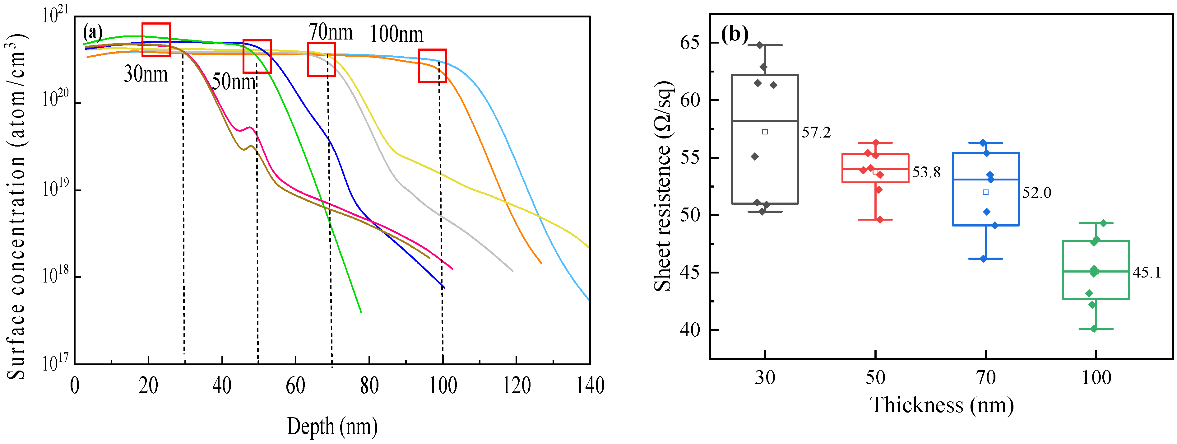
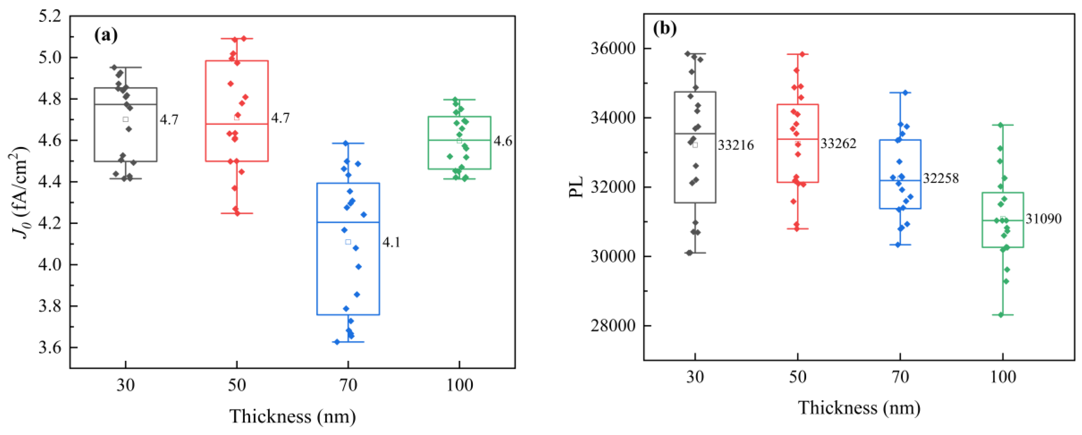
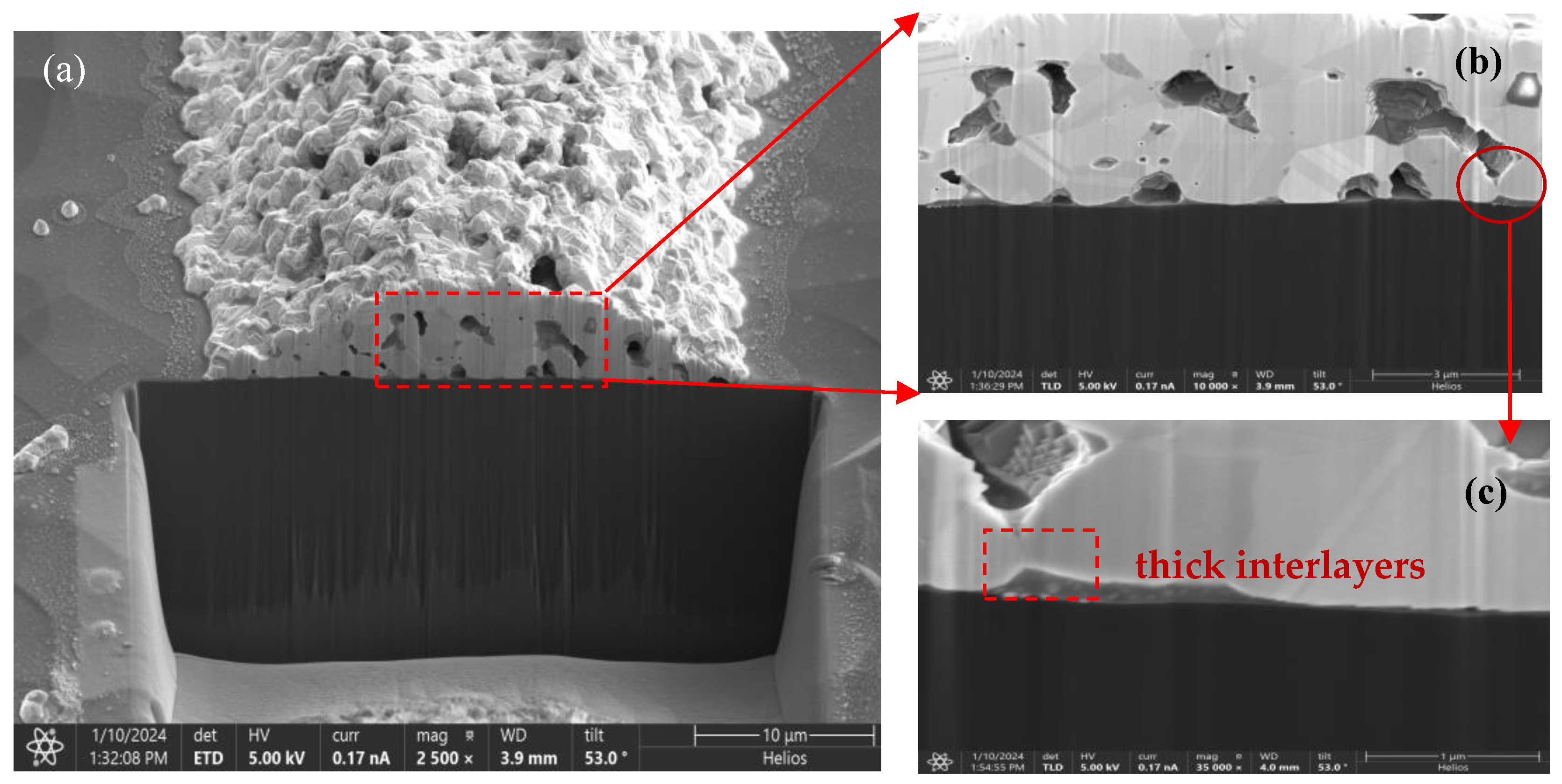
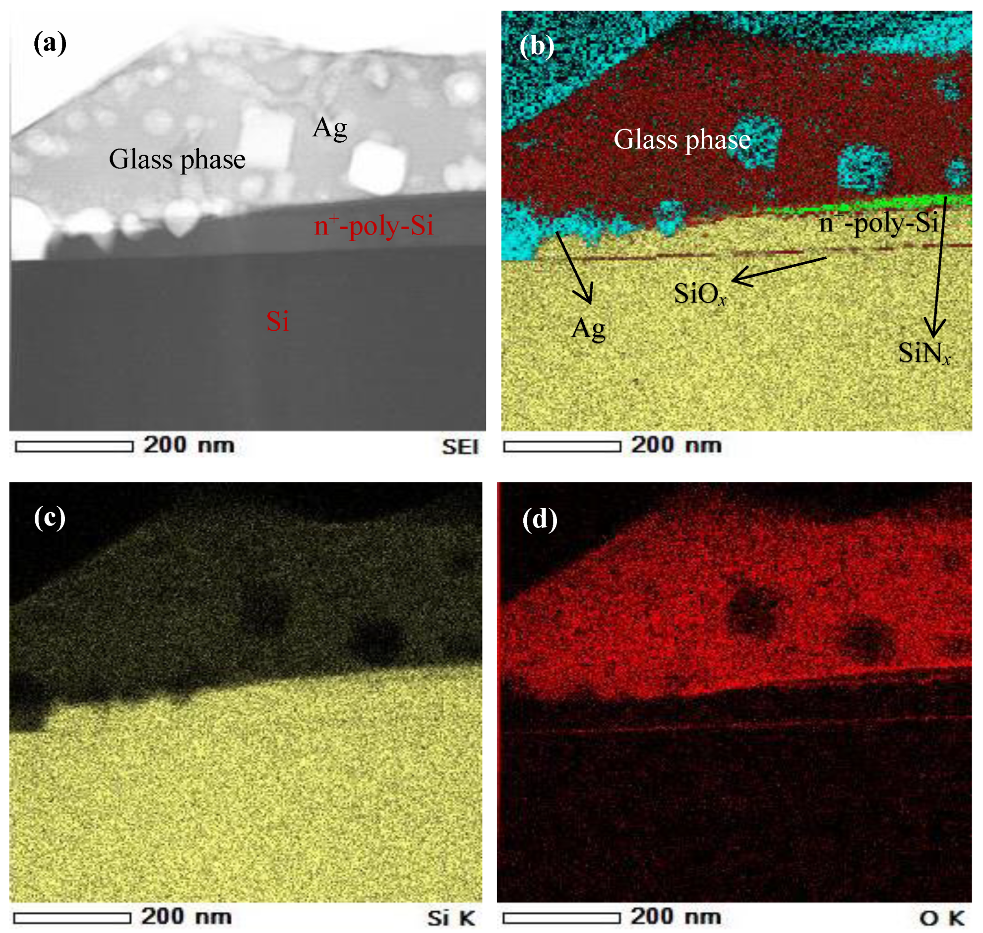
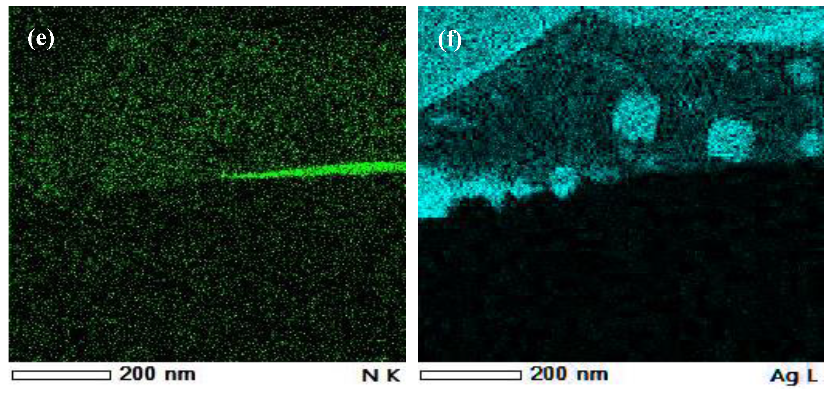
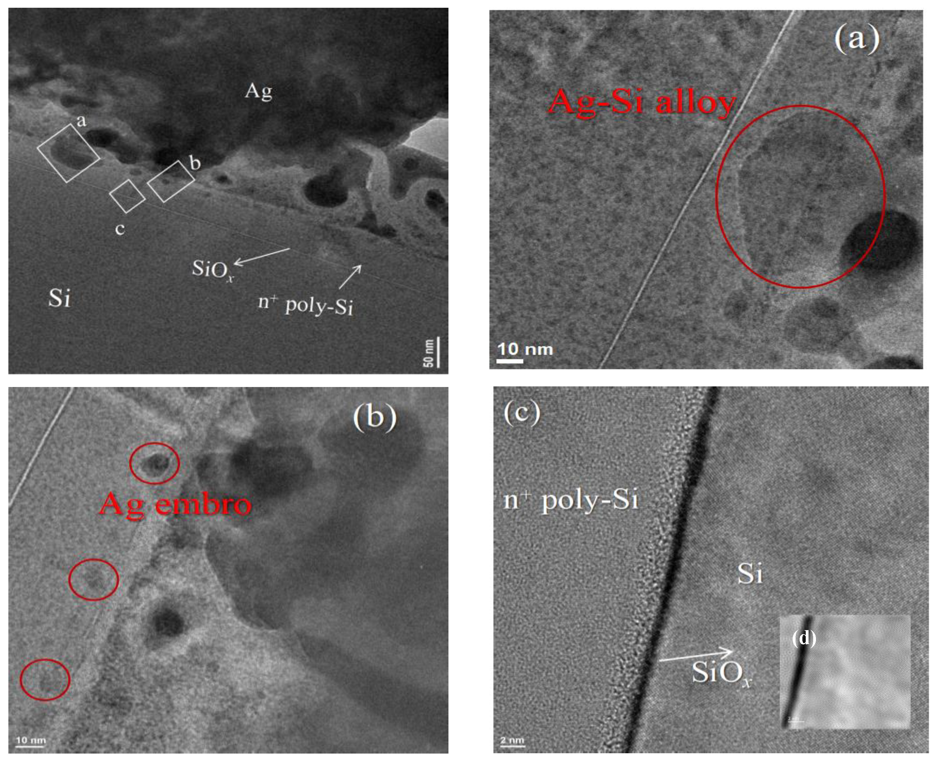
3.1. Microstructure and Performance
3.2. I–V Parameters
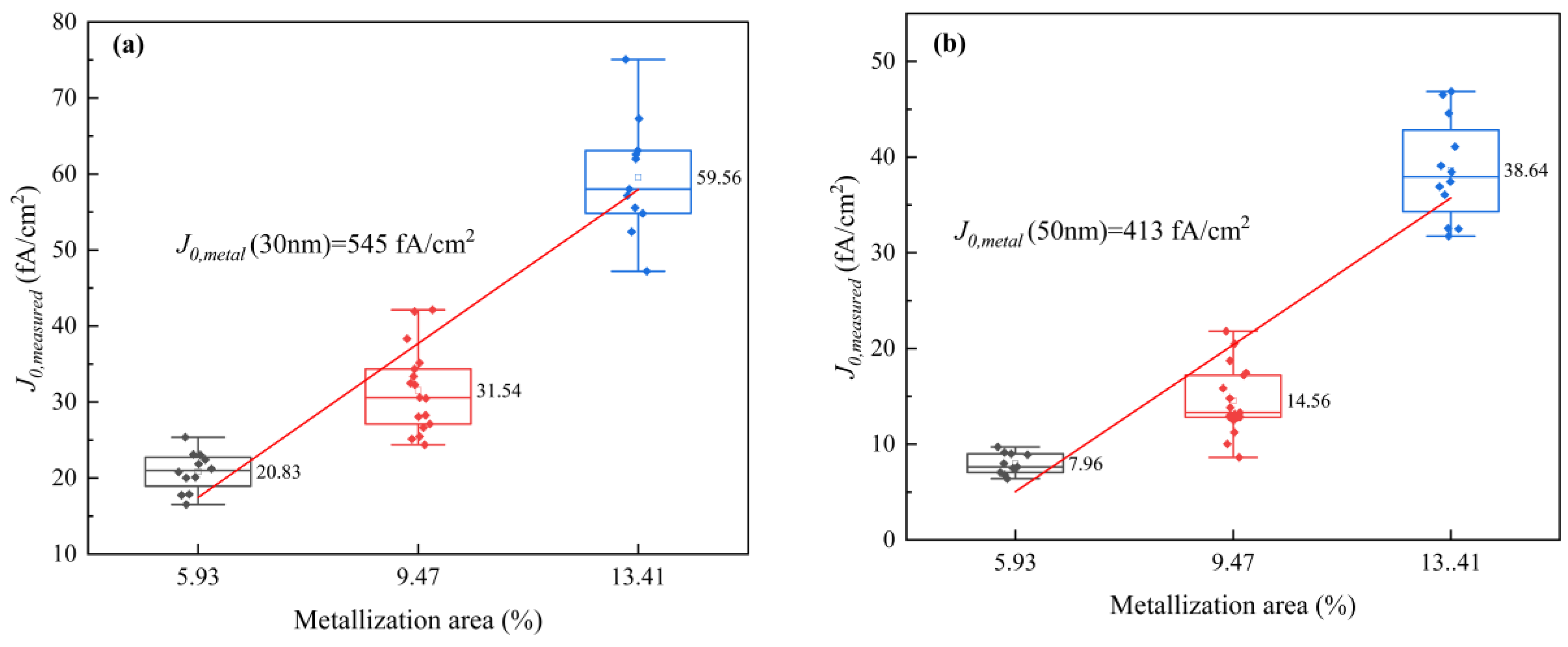
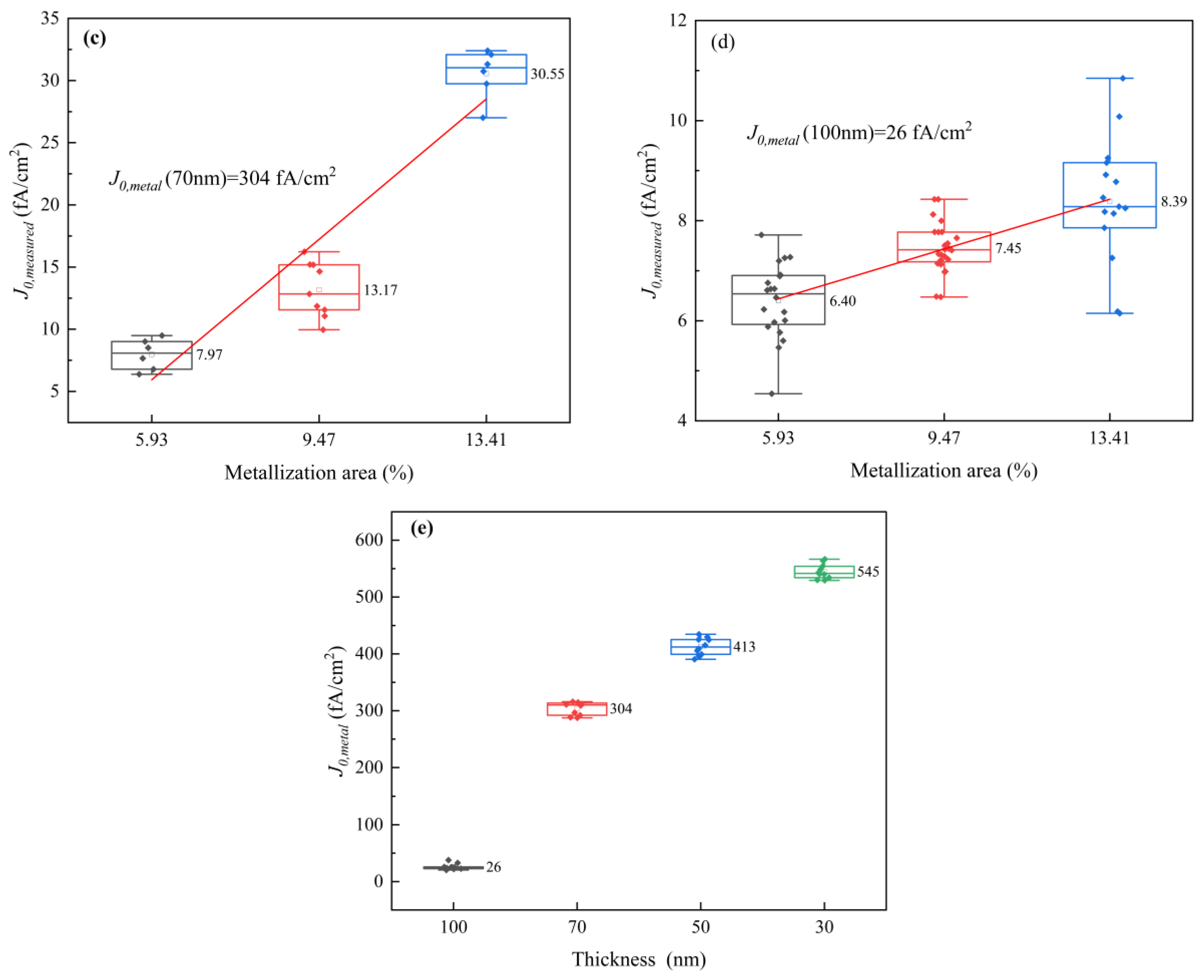
3.3. Failure Analysis
4. Conclusions
Author Contributions
Funding
Institutional Review Board Statement
Informed Consent Statement
Data Availability Statement
Conflicts of Interest
References
- Ullah, H.; Czapp, S.; Szultka, S.; Tariq, H.; Qasim, U.B.; Imran, H. Crystalline Silicon (c-Si)-Based Tunnel Oxide Passivated Contact (TOPCon) Solar Cells: A Review. Energies 2023, 16, 715. [Google Scholar] [CrossRef]
- Fischer, M.; Woodhouse, M.; Herritsch, S.; Trube, J. International Technology Roadmap for Photovoltaic (ITRPV), 14th ed.; VDMA German Engineering Federation: Frankfurt am Main, Germany, 2023. [Google Scholar]
- Jinko (n.d.). High-Efficiency N-Type Monocrystalline Silicon Solar Cell Sets Our New Record with Maximum Conversion Efficiency of 26.4%; Jinko Solar’s: Zhejiang, China, 2023. [Google Scholar]
- Hermle, M.; Feldmann, F.; Bivour, M.; Goldschmidt, J.C.; Glunz, S.W. Passivating contacts and tandem concepts: Approaches for the highest silicon-based solar cell efficiencies. Appl. Phys. Rev. 2020, 7, 021305. [Google Scholar] [CrossRef]
- Nemeth, B.; Young, D.L.; Page, M.R.; LaSalvia, V.; Johnston, S.; Reedy, R.; Stradins, P. Polycrystalline silicon passivated tunneling contacts for high efficiency silicon solar cells. J. Mater. Res. 2016, 31, 671. [Google Scholar] [CrossRef]
- Ng, K.K.; Card, H.C. Asymmetry in the SiO2 tunneling barriers to electrons and holes. J. Appl. Phys. 1980, 51, 2153–2157. [Google Scholar] [CrossRef]
- Chhetri, N.; Das, G.; Kole, A.; Saha, H.; Haldar, S.; Chatterjee, S. P-type polycrystalline silicon seed layer fabrication using RF-PECVD for thin film solar cells. Mater. Today Proc. 2022, 58, 665–667. [Google Scholar] [CrossRef]
- Stöhr, M.; Aprojanz, J.; Brendel, R.; Dullweber, T. Firing-stable PECVD SiOxNy/n-Poly-Si surface passivation for silicon solar cells. ACS Appl. Energy Mater. 2021, 4, 4646–4653. [Google Scholar] [CrossRef]
- Fırat, M.; Radhakrishnan, H.S.; Payo, M.R.; Choulat, P.; Badran, H.; van der Heide, A.; Govaerts, J.; Duerinckx, F.; Tous, L.; Hajjiah, A.; et al. Large-area bifacial n-TOPCon solar cells with in situ phosphorus-doped LPCVD poly-Si passivating contacts. Sol. Energy Mater. Sol. Cells 2022, 236, 111544. [Google Scholar] [CrossRef]
- Stuckelberger, J.; Yan, D.; Phang, S.P.; Samundsett, C.; Wang, J.; Antognini, L.; Haug, F.J.; Wang, Z.; Yang, J.; Zheng, P.; et al. Pre-annealing for improved LPCVD deposited boron-doped poly-Si hole-selective contacts. Sol. Energy Mater. Sol. Cells 2023, 251, 112123. [Google Scholar] [CrossRef]
- Mousumi, J.F.; Gregory, G.; Ganesan, J.P.; Nunez, C.; Provancha, K.; Seren, S.; Zunft, H.; Jurca, T.; Banerjee, P.; Kar, A.; et al. Process–structure–properties relationships of passivating, electron-selective contacts formed by atmospheric pressure chemical vapor deposition of phosphorus-doped polysilicon. Phys. Status Solidi RRL—Rapid Res. Lett. 2022, 16, 2100639. [Google Scholar] [CrossRef]
- Li, S.; Pomaska, M.; Hoß, J.; Lossen, J.; Pennartz, F.; Nuys, M.; Hong, R.; Schmalen, A.; Wolff, J.; Finger, F.; et al. Poly-Si/SiO x /c-Si passivating contact with 738 mV implied open circuit voltage fabricated by hot-wire chemical vapor deposition. Appl. Phys. Lett. 2019, 114, 153901. [Google Scholar] [CrossRef]
- Ingenito, A.; Allebé, C.; Libraro, S.; Ballif, C.; Paviet-Salomon, B.; Nicolay, S.; Leon, J.J.D. 22.8% full-area bifacial n-PERT solar cells with rear side sputtered poly-Si(n) passivating contact. Sol. Energy Mater. Sol. Cells 2023, 249, 112043. [Google Scholar] [CrossRef]
- Nasebandt, L.; Min, B.; Hollemann, C.; Hübner, S.; Dippell, T.; Peibst, R.; Brendel, R. Sputtered phosphorus-doped poly-Si on oxide contacts for screen-printed Si solar cells. Sol. RRL 2022, 6, 2200409. [Google Scholar] [CrossRef]
- Sedani, S.H.; Yasar, O.F.; Karaman, M.; Turan, R. Effects of boron doping on solid phase crystallization of in situ doped amorphous Silicon thin films prepared by electron beam evaporation. Thin Solid Films 2020, 694, 137639. [Google Scholar] [CrossRef]
- Kafle, B.; Goraya, B.S.; Mack, S.; Feldmann, F.; Nold, S.; Rentsch, J. TOPCon-technology options for cost efficient industrial manufacturing. Sol. Energy Mater. Sol. Cells 2021, 227, 111100. [Google Scholar] [CrossRef]
- Truong, T.N.; Yan, D.; Nguyen, C.P.T.; Kho, T.; Guthrey, H.; Seidel, J.; Al-Jassim, M.; Cuevas, A.; Macdonald, D.; Nguyen, H.T. Microstructure, and doping behaviour: A comparison between different deposition methods for poly-Si/SiOx passivating contacts. Prog. Photovolt. Res. Appl. 2021, 29, 857–868. [Google Scholar] [CrossRef]
- Yan, D.; Cuevas, A.; Michel, J.I.; Zhang, C.; Wan, Y.; Zhang, X.; Bullock, J. Polysilicon passivated junctions: The next technology for silicon solar cells? Joule 2021, 5, 811–828. [Google Scholar] [CrossRef]
- Chen, D.; Chen, Y.; Wang, Z.; Gong, J.; Liu, C.; Zou, Y.; He, Y.; Wang, Y.; Yuan, L.; Lin, W.; et al. 24.58% total area efffciency of screen-printed, large area industrial silicon solar cells with the tunnel oxide passivated contacts (i-TOPCon) design. Sol. Energy Mater. Sol. Cells 2020, 206, 110258. [Google Scholar] [CrossRef]
- Chen, Y.; Chen, D.; Liu, C.; Wang, Z.; Zou, Y.; He, Y.; Wang, Y.; Yuan, L.; Gong, J.; Lin, W.; et al. Mass production of industrial tunnel oxide passivated contacts (i-TOPCon) silicon solar cells with average efffciency over 23% and modules over 345 W. Prog. Photovolt. Res. Appl. 2019, 27, 827–834. [Google Scholar] [CrossRef]
- Stodolny, M.K.; Lenes, M.; Wu, Y.; Janssen, G.J.M.; Romijn, I.G.; Luchies, J.R.M.; Geerligs, L.J. n-Type polysilicon passivating contact for industrial bifacial n-type solar cells. Sol. Energy Mater. Sol. Cells 2016, 158, 24–28. [Google Scholar] [CrossRef]
- Stodolny, M.K.; Anker, J.; Geerligs, B.L.; Janssen, G.J.; Van De Loo, B.W.; Melskens, J.; Santbergen, R.; Isabella, O.; Schmitz, J.; Lenes, M.; et al. Material properties of LPCVD processed n-type polysilicon passivating contacts and its application in PERPoly industrial bifacial solar cells. In Energy Procedia; Elsevier Ltd.: Amsterdam, The Netherlands, 2017; pp. 635–642. [Google Scholar]
- Padhamnath, P.; Buatis, J.K.; Khanna, A.; Nampalli, N.; Nandakumar, N.; Shanmugam, V.; Aberle, A.G.; Duttagupta, S. Characterization of screen printed and ffre-through contacts on LPCVD based passivating contacts in monoPolyTM solar cells. Sol. Energy 2020, 202, 73–79. [Google Scholar] [CrossRef]
- Padhamnath, P.; Khanna, A.; Nandakumar, N.; Nampalli, N.; Shanmugam, V.; Aberle, A.G.; Duttagupta, S. Development of thin polysilicon layers for application in monoPolyTM cells with screen-printed and fired metallization. Sol. Energy Mater. Sol. Cells 2020, 207, 110358. [Google Scholar] [CrossRef]
- Learn, A.J.; Foster, D.W. Deposition and electrical properties of in situ phosphorusdoped silicon fflms formed by low-pressure chemical vapor deposition. J. Appl. Phys. 1987, 61, 1898–1904. [Google Scholar] [CrossRef]
- Meyerson, B.S.; Olbricht, W. Phosphorus-doped polycrystalline silicon via LPCVD: I. Process characterization. J. Electrochem. Soc. 1984, 131, 2361–2365. [Google Scholar] [CrossRef]
- Meyerson, B.S.; Yu, M.L. Phosphorus-doped polycrystalline silicon via LPCVD: II. Surface interactions of the silane/phosphine/silicon system. J. Electrochem. Soc. 1984, 131, 2366–2368. [Google Scholar] [CrossRef]
- Mulder, J.G.M.; Eppenga, P.; Hendriks, M.; Tong, J.E. An industrial LPCVD process for in situ phosphorus-doped polysilicon. J. Electrochem. Soc. 1990, 137, 273–279. [Google Scholar] [CrossRef]
- Ahmed, W.; Ahmed, E. An investigation of LPCVD and PECVD of in situ doped polycrystalline silicon for VLSI. Adv. Mater. Opt. Electron. 1992, 1, 255–259. [Google Scholar] [CrossRef]
- Qiu, K.; Pomaska, M.; Li, S.; Lambertz, A.; Duan, W.; Gad, A.; Geitner, M.; Brugger, J.; Liang, Z.; Shen, H.; et al. Development of conductive SiCx:H as a new hydrogenation technique for tunnel oxide passivating contacts. ACS Appl. Mater. Interfaces 2020, 12, 29986–29992. [Google Scholar] [CrossRef] [PubMed]
- Yang, Q.; Liu, Z.; Lin, Y.; Liu, W.; Liao, M.; Feng, M.; Zhi, Y.; Zheng, J.; Lu, L.; Ma, D.; et al. Passivating contact with phosphorus-doped polycrystalline silicon-nitride with an excellent implied open-circuit voltage of 745 mV and its application in 23.88% efffciency TOPCon solar cells. Sol. RRL 2021, 5, 2100644. [Google Scholar] [CrossRef]
- Römer, U.; Peibst, R.; Ohrdes, T.; Lim, B.; Krügener, J.; Wietler, T.; Brendel, R. Ion implantation for poly-Si passivated back-junction back-contacted solar cells. IEEE J. Photovolt. 2015, 5, 507–514. [Google Scholar] [CrossRef]
- Zheng, P.; Yang, J.; Wang, Z.; Wu, L.; Sun, H.; Chen, S.; Guo, Y.; Xia, H.; Phang, S.P.; Wang, E.C.; et al. Detailed loss analysis of 24.8% large-area screen-printed n-type solar cell with polysilicon passivating contact. Cell Rep. Phys. Sci. 2021, 2, 100603. [Google Scholar] [CrossRef]
- Wu, W.F.; Tsai, K.C.; Chao, C.G.; Chen, J.C.; Ou, K.L. Novel multilayered Ti/TiN diffusion barrier for Al metallization. J. Electron. Mater. 2005, 34, 1150–1156. [Google Scholar] [CrossRef]
- Yu, J.; Chen, Y.; He, J.; Bai, Y.; Su, R.; Cao, T.; Liu, W.; Chen, T. Enhancing poly-Si contact through a highly conductive and ultra-thin TiN layer for high-efficiency passivating contact silicon solar cells. Sol. Energy Mater. Sol. Cells 2023, 260, 112491. [Google Scholar] [CrossRef]
- Morales-Vilches, A.B.; Larionova, Y.; Wietler, T.; Cruz, A.; Korte, L.; Peibst, R.; Brendel, R.; Schlatmann, R.; Stannowski, B. ZnO: Al/a-SiOx front contact for polycrystalline-silicon-on-oxide (POLO) solar cells. In AIP Conference Proceedings; AIP Publishing: Melville, NY, USA, 2018. [Google Scholar]
- Adachi, D.; Terashita, T.; Uto, T.; Hernández, J.L.; Yamamoto, K. Effects of SiOx barrier layer prepared by plasma-enhanced chemical vapor deposition on improvement of long-term reliability and production cost for Cu-plated amorphous Si/crystalline Si heterojunction solar cells. Sol. Energy Mater. Sol. Cells 2017, 163, 204–209. [Google Scholar] [CrossRef]
- Fellmeth, T.; Höffler, H.; Mack, S.; Krassowski, E.; Krieg, K.; Kafle, B.; Greulich, J. Laser-enhanced contact optimization on iTOPCon solar cells. Prog. Photovolt. Res. Appl. 2022, 23630, 1393–1399. [Google Scholar] [CrossRef]
- Chaudhary, A.; Hoß, J.; Lossen, J.; Huster, F.; Kopecek, R.; van Swaaij, R.; Zeman, M. Influence of polysilicon thickness on properties of screen-printed silver paste metallized silicon oxide/polysilicon passivated contacts. Phys. Status Solidi (a) 2021, 218, 2100243. [Google Scholar] [CrossRef]
- Meyer, F.; Ingenito, A.; Leon, J.J.D.; Niquille, X.; Allebé, C.; Nicolay, S.; Haug, F.J.; Ballif, C. Localisation of front side passivating contacts for direct metallisation of high-efficiency c-Si solar cells. Sol. Energy Mater. Sol. Cells 2022, 235, 111455. [Google Scholar] [CrossRef]
- Çiftpınar, H.E.; Stodolny, M.K.; Wu, Y.; Janssen, G.J.; Löffler, J.; Schmitz, J.; Lenes, M.; Luchies, J.M.; Geerligs, L.J. Study of screen printed metallization for polysilicon based passivating contacts. Energy Procedia 2017, 124, 851–861. [Google Scholar] [CrossRef]
- Wang, Q.; Wu, W.; Li, Y.; Yuan, L.; Yang, S.; Sun, Y.; Yang, S.; Zhang, Q.; Cao, Y.; Qu, H.; et al. Impact of boron doping on electrical performance and efficiency of n-TOPCon solar cell. Sol. Energy 2021, 227, 273–291. [Google Scholar] [CrossRef]
- Wang, Q.; Peng, H.; Gu, S.; Guo, K.; Wu, W.; Li, B.; Li, L.; Yuan, N.; Ding, J. High-efficiency n-TOPCon bifacial solar cells with selective poly-Si based passivating contacts. Sol. Energy Mater. Sol. Cells 2023, 259, 112458. [Google Scholar] [CrossRef]
- Wang, Q.; Yuan, L.; Li, L.; Peng, H.; Li, B.; Wang, A.; Zhang, L.; Wu, W.; Ding, J.; Yuan, N. Boron tube diffusion process parameters for high-efficiency n-TOPCon solar cells with selective boron emitters. Sol. Energy Mater. Sol. Cells 2023, 253, 112231. [Google Scholar] [CrossRef]
- Liu, B.; Chen, Y.; Yang, Y.; Chen, D.; Feng, Z.; Altermatt, P.P.; Verlinden, P.; Shen, H. Improved evaluation of saturation currents and bulk lifetime in industrial Si solar cells by the quasi steady state photo conductance decay method. Sol. Energy Mater. Sol. Cells 2016, 149, 258–265. [Google Scholar] [CrossRef]
- Yablonovitch, E. Statistical ray optics. J. Opt. Soc. Am. 1987, 72, 899–907. [Google Scholar] [CrossRef]
- Allen, T.G.; Bullock, J.; Yang, X.; Javey, A.; De Wolf, S. Passivating contacts for crystalline silicon solar cells. Nat. Energy 2019, 4, 914–928. [Google Scholar] [CrossRef]
- Wang, Q.; Wu, W.; Chen, D.; Yuan, L.; Yang, S.; Sun, Y.; Zhang, Q.; Cao, Y.; Qu, H.; Yuan, N.; et al. Study on the cleaning process of n+-poly-Si wraparound removal of TOPCon solar cells. Sol. Energy 2020, 211, 324–335. [Google Scholar] [CrossRef]


| Conditions (Poly Thickness) | SiOx Layer Formation Process | a-Si Layer Formation Process | Phosphorus Doped Poly-Si Layer Formation Process | Main Result Data | |||||||||
|---|---|---|---|---|---|---|---|---|---|---|---|---|---|
| toxidation (min) | T (°C) | t (min) | GSiH4 (sccm) | ECV (nm) | Tdeposition (°C) | GPOCl3 (sccm) | Tdrive-in (°C) | R□ (Ω/sq) | ρc (mΩ·cm2) | J0 (fA/cm2) | PL (a.u) | J0,metal (fA/cm2) | |
| 100 nm | 8 | 600 | 24 | 850 | 100 | 850 | 1100–1200 | 850–860 | 45 | 2.5 | 4.6 | 31,090 | 26 |
| 70 nm | 19 | 70 | 52 | 2.9 | 4.1 | 32,258 | 304 | ||||||
| 50 nm | 16 | 50 | 54 | 3.5 | 4.7 | 33,262 | 413 | ||||||
| 30 nm | 13 | 30 | 57 | 3.9 | 4.7 | 33,216 | 545 | ||||||
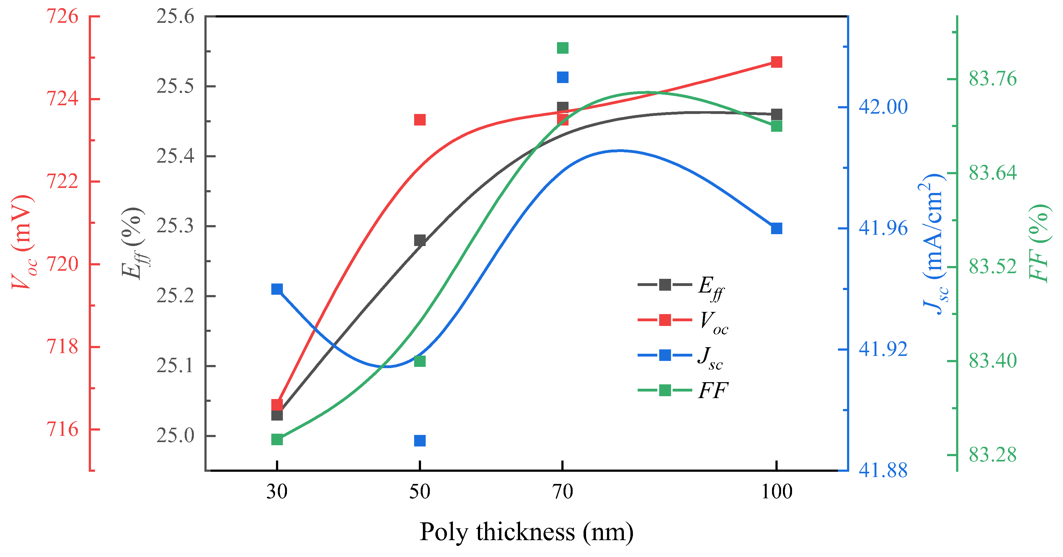
| Poly Thickness (nm) | Eff (%) | Voc (mV) | Jsc (mA/cm2) | FF (%) | Cell Area (cm2) |
|---|---|---|---|---|---|
| 30 | 25.03 | 716.6 | 41.94 | 83.3 | 334.88 |
| 50 | 25.27 | 723.5 | 41.89 | 83.4 | |
| 70 | 25.47 | 723.5 | 42.01 | 83.8 | |
| 100 | 25.46 | 724.9 | 41.96 | 83.7 |
Disclaimer/Publisher’s Note: The statements, opinions and data contained in all publications are solely those of the individual author(s) and contributor(s) and not of MDPI and/or the editor(s). MDPI and/or the editor(s) disclaim responsibility for any injury to people or property resulting from any ideas, methods, instructions or products referred to in the content. |
© 2024 by the authors. Licensee MDPI, Basel, Switzerland. This article is an open access article distributed under the terms and conditions of the Creative Commons Attribution (CC BY) license (https://creativecommons.org/licenses/by/4.0/).
Share and Cite
Wang, Q.; Gao, B.; Wu, W.; Guo, K.; Huang, W.; Ding, J. Effects on Metallization of n+-Poly-Si Layer for N-Type Tunnel Oxide Passivated Contact Solar Cells. Materials 2024, 17, 2747. https://doi.org/10.3390/ma17112747
Wang Q, Gao B, Wu W, Guo K, Huang W, Ding J. Effects on Metallization of n+-Poly-Si Layer for N-Type Tunnel Oxide Passivated Contact Solar Cells. Materials. 2024; 17(11):2747. https://doi.org/10.3390/ma17112747
Chicago/Turabian StyleWang, Qinqin, Beibei Gao, Wangping Wu, Kaiyuan Guo, Wei Huang, and Jianning Ding. 2024. "Effects on Metallization of n+-Poly-Si Layer for N-Type Tunnel Oxide Passivated Contact Solar Cells" Materials 17, no. 11: 2747. https://doi.org/10.3390/ma17112747
APA StyleWang, Q., Gao, B., Wu, W., Guo, K., Huang, W., & Ding, J. (2024). Effects on Metallization of n+-Poly-Si Layer for N-Type Tunnel Oxide Passivated Contact Solar Cells. Materials, 17(11), 2747. https://doi.org/10.3390/ma17112747