


Threshold-Voltage Extraction Methods for Atomically Deposited Disordered ZnO Thin-Film Transistors
Abstract
1. Introduction
2. Materials and Methods
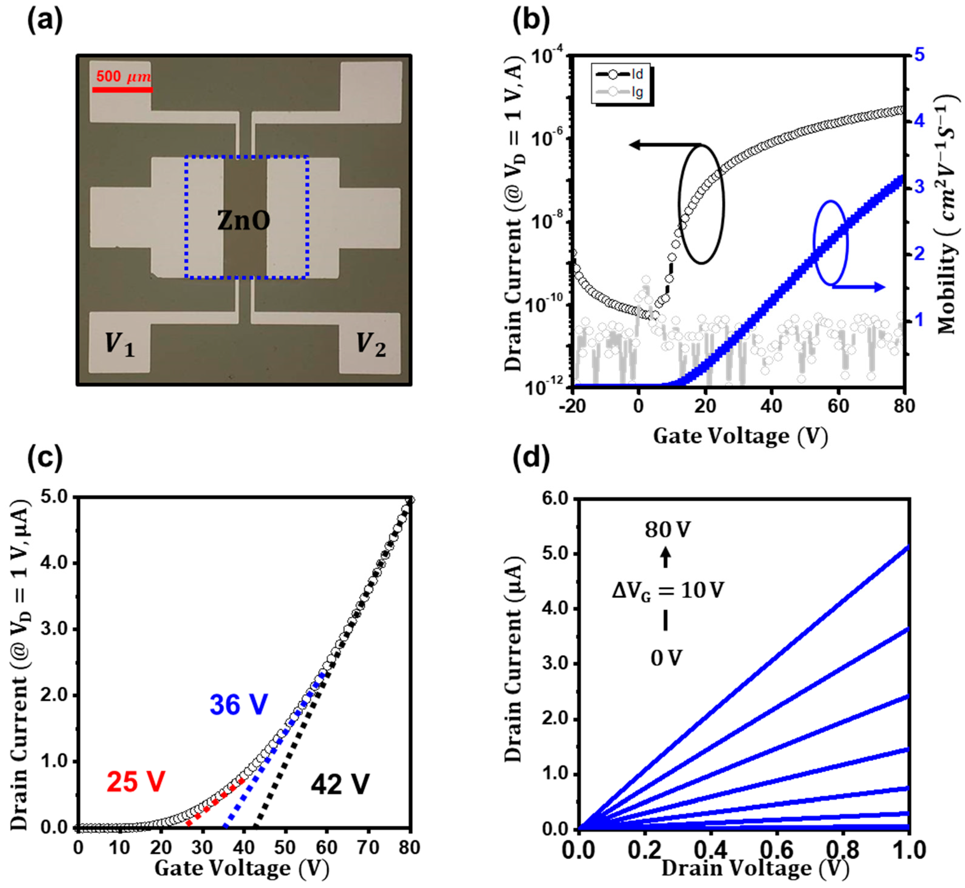
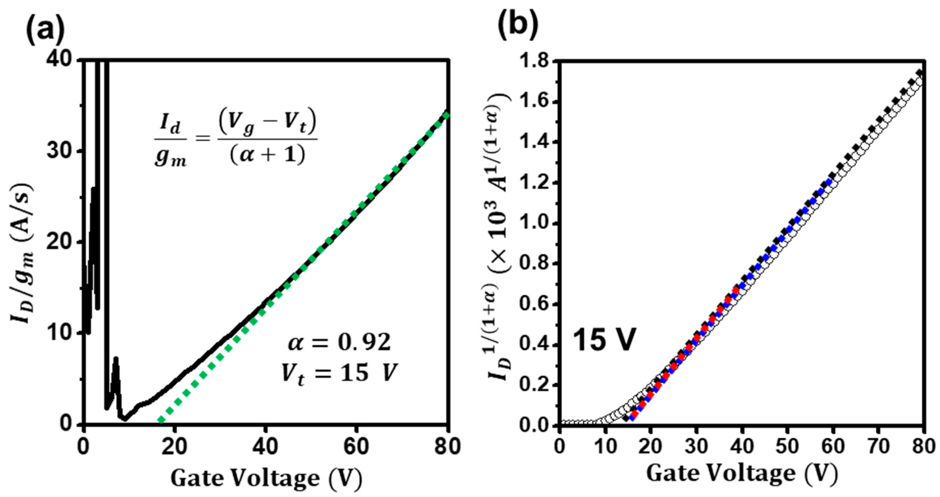
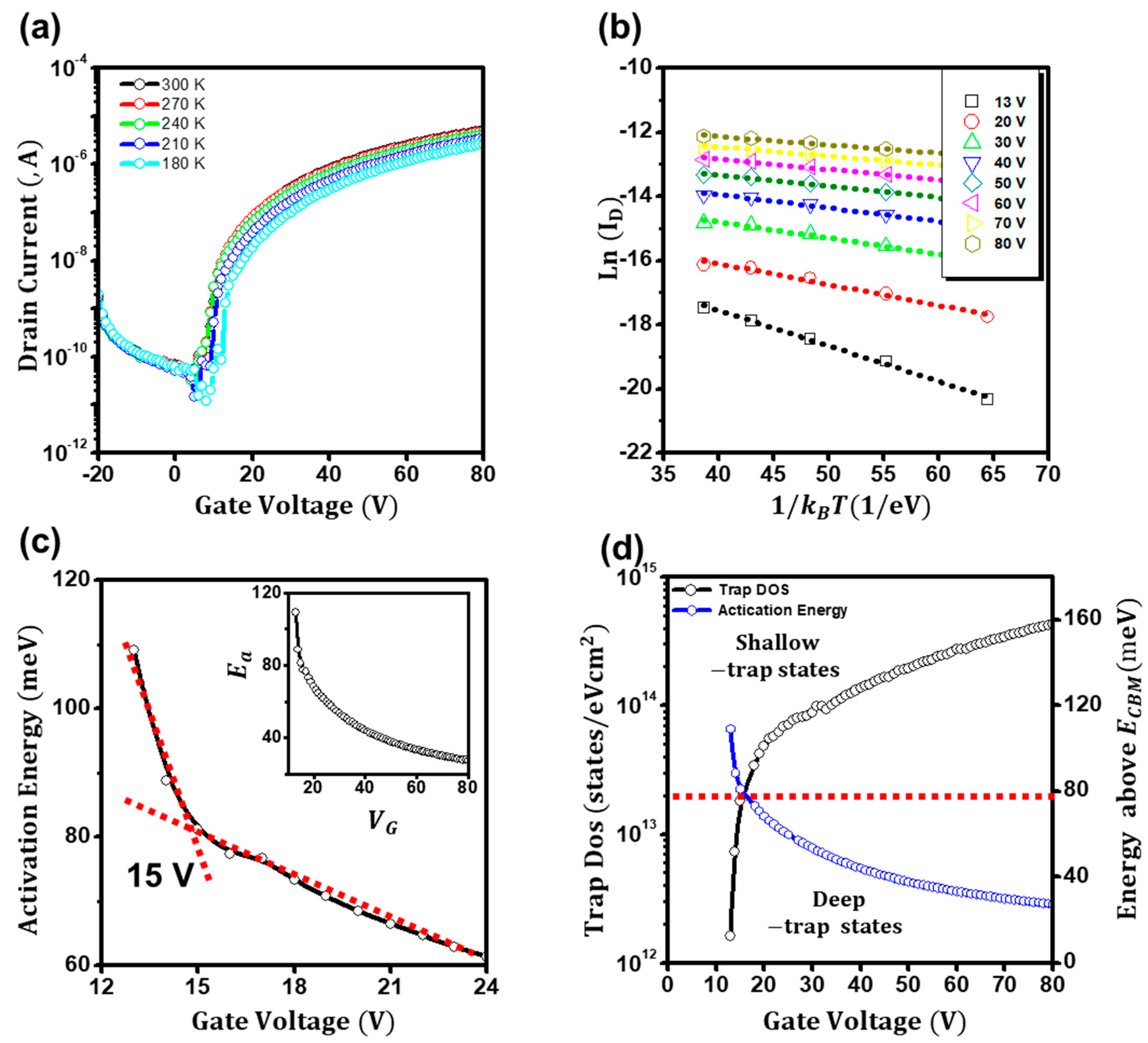
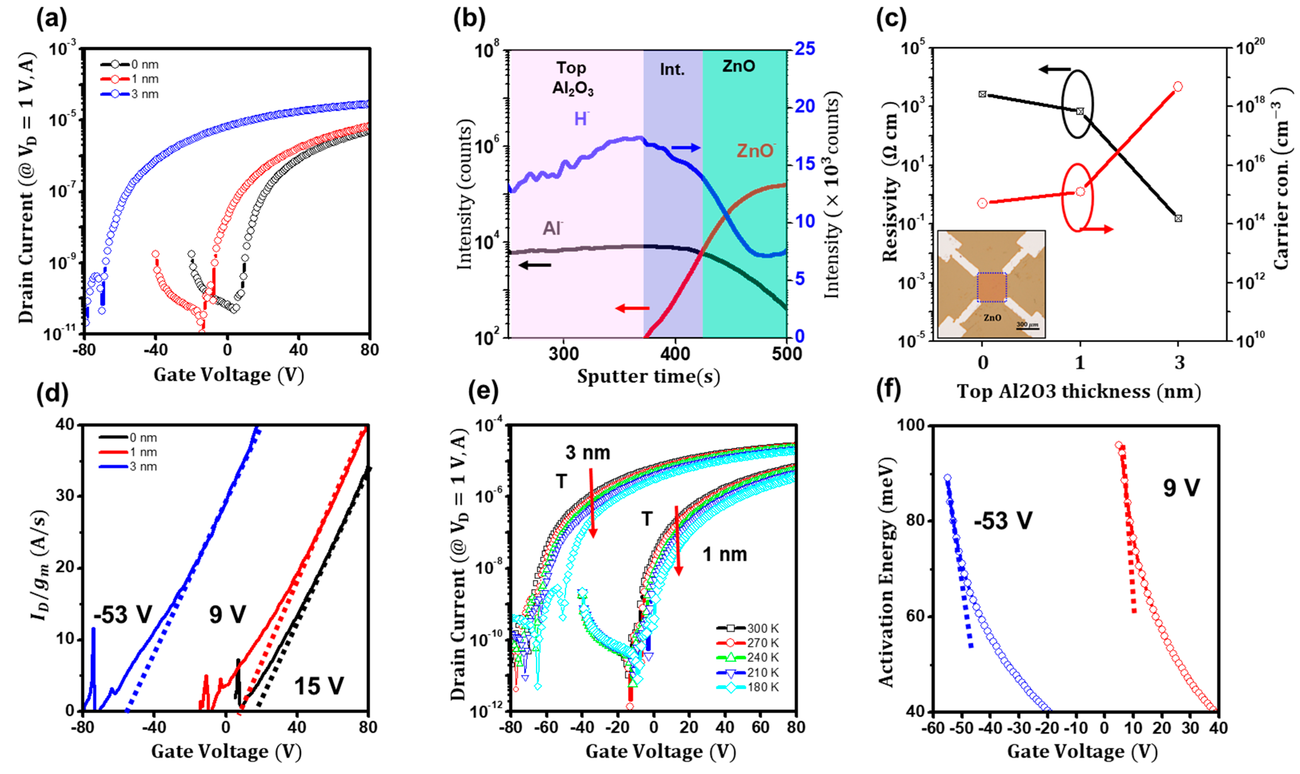
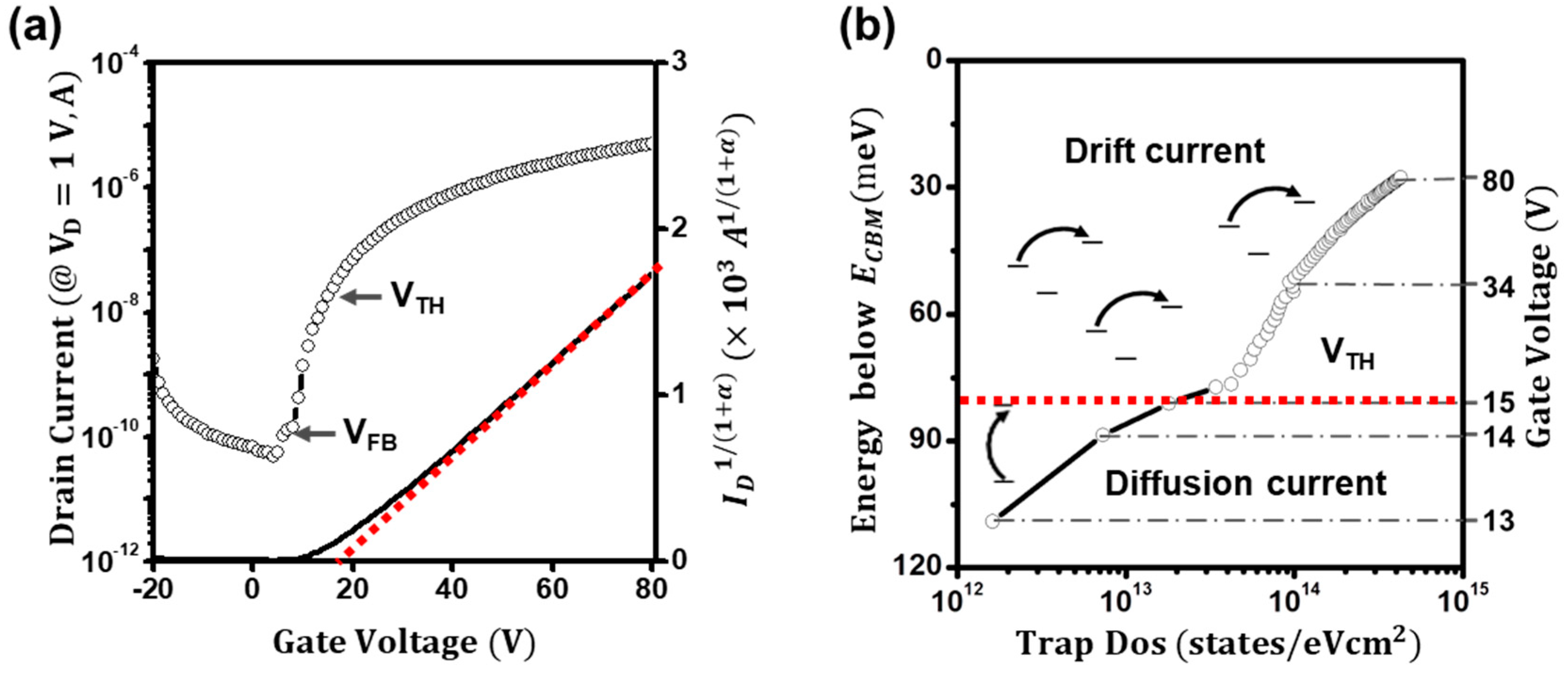
3. Results
4. Discussion
5. Conclusions
Supplementary Materials
Funding
Institutional Review Board Statement
Informed Consent Statement
Data Availability Statement
Conflicts of Interest
References
- Kim, S.; Kwon, H.J.; Lee, S.; Shim, H.; Chun, Y.; Choi, W.; Kwack, J.; Han, D.; Song, M.; Kim, S.; et al. Low-Power Flexible Organic Light-Emitting Diode Display Device. Adv. Mater. 2011, 23, 3511–3516. [Google Scholar] [CrossRef] [PubMed]
- Rogers, J.A.; Someya, T.; Huang, Y. Materials and Mechanics for Stretchable Electronics. Science 2010, 327, 1603–1607. [Google Scholar] [CrossRef] [PubMed]
- Xu, R.P.; Li, Y.Q.; Tang, J.X. Recent Advances in Flexible Organic Light-Emitting Diodes. J. Mater. Chem. C 2016, 4, 9116–9142. [Google Scholar] [CrossRef]
- Zhang, J.; Li, Y.; Zhang, B.; Wang, H.; Xin, Q.; Song, A. Flexible Indium-Gallium-Zinc-Oxide Schottky Diode Operating beyond 2.45 GHz. Nat. Commun. 2015, 6, 7561. [Google Scholar] [CrossRef]
- Ono, S.; Miwa, K.; Maekawa, Y.; Tsujimura, T. VT Compensation Circuit for AM OLED Displays Composed of Two TFTs and One Capacitor. IEEE Trans. Electron Devices 2007, 54, 462–467. [Google Scholar] [CrossRef]
- Li, Q.; Lee, C.-H.; Asad, M.; Wong, W.S.; Sachdev, M. A 6-TFT Charge-Transfer Self-Compensating Pixel Circuit for Flexible Displays. IEEE J. Electron Devices Soc. 2019, 7, 792–800. [Google Scholar] [CrossRef]
- Anzi, L.; Tuktamyshev, A.; Fedorov, A.; Zurutuza, A.; Sanguinetti, S.; Sordan, R. Controlling the Threshold Voltage of a Semiconductor Field-Effect Transistor by Gating Its Graphene Gate. npj 2d Mater. Appl. 2022, 6, 28. [Google Scholar] [CrossRef]
- Chen, C.L.; Chen, W.F.; Zhou, L.; Wu, W.J.; Xu, M.; Wang, L.; Peng, J.B. A Physics-Based Model of Threshold Voltage for Amorphous Oxide Semiconductor Thin-Film Transistors. AIP Adv. 2016, 6, 035025. [Google Scholar] [CrossRef]
- Lee, S.; Nathan, A. Conduction Threshold in Accumulation-Mode InGaZnO Thin Film Transistors. Sci. Rep. 2016, 6, 22567. [Google Scholar] [CrossRef]
- Choi, C.H.; Kim, T.; Ueda, S.; Shiah, Y.S.; Hosono, H.; Kim, J.; Jeong, J.K. High-Performance Indium Gallium Tin Oxide Transistors with an Al2O3Gate Insulator Deposited by Atomic Layer Deposition at a Low Temperature of 150 °C: Roles of Hydrogen and Excess Oxygen in the Al2O3 Dielectric Film. ACS Appl. Mater. Interfaces 2021, 13, 28451–28461. [Google Scholar] [CrossRef]
- Ortiz-Conde, A.; García-Sánchez, F.J.; Muci, J.; Terán Barrios, A.; Liou, J.J.; Ho, C.S. Revisiting MOSFET Threshold Voltage Extraction Methods. Microelectron. Reliab. 2013, 53, 90–104. [Google Scholar] [CrossRef]
- So, M.; Colinge, J. Conduction Mechanisms in Thin-Film Accumulation-mode SOI p-channel MOSFETs. IEEE Trans. Electron Devices 1990, 37, 718–723. [Google Scholar]
- Liang, K.; Xu, X.; Zhou, Y.; Wang, X.; McCulley, C.M.; Wang, L.; Kulkarni, J.; Dodabalapur, A. Nanospike Electrodes and Charge Nanoribbons: A New Design for Nanoscale Thin-Film Transistors. Sci. Adv. 2022, 8, eabm1154. [Google Scholar] [CrossRef] [PubMed]
- Tang, Z.; Wie, C.R. Capacitance-Voltage Characteristics and Device Simulation of Bias Temperature Stressed a-Si:H TFTs. Solid. State. Electron. 2010, 54, 259–267. [Google Scholar] [CrossRef]
- Kamiya, T.; Nomura, K.; Hosono, H. Origins of High Mobility and Low Operation Voltage of Amorphous Oxide TFTs: Electronic Structure, Electron Transport, Defects and Doping*. J. Disp. Technol. 2009, 5, 468–483. [Google Scholar] [CrossRef]
- Guo, J.; Zhao, Y.; Yang, G.; Chuai, X.; Lu, W.; Liu, D.; Chen, Q.; Duan, X.; Huang, S.; Su, Y.; et al. Analytical Surface Potential-Based Compact Model for Independent Dual Gate a-IGZO TFT. IEEE Trans. Electron Devices 2021, 68, 2049–2055. [Google Scholar] [CrossRef]
- Horowitz, G.; Delannoy, P. An Analytical Model for Organic-Based Thin-Film Transistors. J. Appl. Phys. 1991, 70, 469–475. [Google Scholar] [CrossRef]
- Lu, N.; Jiang, W.; Wu, Q.; Geng, D.; Li, L.; Liu, M. A Review for Compact Model of Thin-Film Transistors (TFTs). Micromachines 2018, 9, 599. [Google Scholar] [CrossRef]
- Migliorato, P.; Seok, M.; Jang, J. Determination of Flat Band Voltage in Thin Film Transistors: The Case of Amorphous-Indium Gallium Zinc Oxide. Appl. Phys. Lett. 2012, 100, 073506. [Google Scholar] [CrossRef]
- Campbell, A.J.; Rawcliffe, R.; Guite, A.; Faria, J.C.D.; Mukherjee, A.; McLachlan, M.A.; Shkunov, M.; Bradley, D.D.C. Charge-Carrier Density Independent Mobility in Amorphous Fluorene-Triarylamine Copolymers. Adv. Funct. Mater. 2016, 26, 3720–3729. [Google Scholar] [CrossRef]
- Jung, S.; Jin, J.W.; Mosser, V.; Bonnassieux, Y.; Horowitz, G. A Compact Model and Parameter Extraction Method for a Staggered OFET with Power-Law Contact Resistance and Mobility. IEEE Trans. Electron Devices 2019, 66, 4894–4900. [Google Scholar] [CrossRef]
- Yoon, M.; Lee, J. Intrinsic Device Parameter Extraction Method for Zinc Oxide-Based Thin-Film Transistors. Appl. Phys. Express 2021, 14, 124003. [Google Scholar] [CrossRef]
- Yoon, M.; Park, J.; Tran, D.C.; Sung, M.M. Fermi-Level Engineering of Atomic Layer-Deposited Zinc Oxide Thin Films for a Vertically Stacked Inverter. ACS Appl. Electron. Mater. 2020, 2, 537–544. [Google Scholar] [CrossRef]
- Li, J.; Ding, X.W.; Zhang, J.H.; Zhang, H.; Jiang, X.Y.; Zhang, Z.L. Improving Electrical Performance and Bias Stability of HfInZnO-TFT with Optimizing the Channel Thickness. AIP Adv. 2013, 3, 102132. [Google Scholar] [CrossRef]
- Kim, H.; Park, J.; Khim, T.; Bak, S.; Song, J.; Choi, B. Threshold Voltage Instability and Polyimide Charging Effects of LTPS TFTs for Flexible Displays. Sci. Rep. 2021, 11, 1–8. [Google Scholar] [CrossRef] [PubMed]
- Pesavento, P.V.; Chesterfield, R.J.; Newman, C.R.; Frisble, C.D. Gated Four-Probe Measurements on Pentacene Thin-Film Transistors: Contact Resistance as a Function of Gate Voltage and Temperature. J. Appl. Phys. 2004, 96, 7312–7324. [Google Scholar] [CrossRef]
- Chen, C.Y.; Kanicki, J. Gated-Four-Probe a-Si:H TFT Structure: A New Technique to Measure the Intrinsic Performance of a-Si:H TFT. IEEE Electron Device Lett. 1997, 18, 340–342. [Google Scholar] [CrossRef]
- Yoon, M.; Lee, J. Enhanced Channel Modulation in Aluminum- and Hydrogen-Doped Zinc-Oxide-Based Transistors by Complementary Dual-Gate Operation. Appl. Surf. Sci. 2022, 585, 152662. [Google Scholar] [CrossRef]
- Kalb, W.L.; Batlogg, B. Calculating the Trap Density of States in Organic Field-Effect Transistors from Experiment: A Comparison of Different Methods. Phys. Rev. B-Condens. Matter Mater. Phys. 2010, 81, 035327. [Google Scholar] [CrossRef]
- Yoon, M.; Lee, J. Charge Transfer Doping with an Organic Layer to Achieve a High-Performance p-Type WSe2 Transistor. J. Mater. Chem. C 2021, 9, 9592–9598. [Google Scholar] [CrossRef]
- Kim, S.; Ha, T.J.; Sonar, P.; Dodabalapur, A. Density of Trap States in a Polymer Field-Effect Transistor. Appl. Phys. Lett. 2014, 105, 133302. [Google Scholar] [CrossRef]
- Geiger, M.; Schwarz, L.; Zschieschang, U.; Manske, D.; Pflaum, J.; Weis, J.; Klauk, H.; Weitz, R.T. Quantitative Analysis of the Density of Trap States in Semiconductors by Electrical Transport Measurements on Low-Voltage Field-Effect Transistors. Phys. Rev. Appl. 2018, 10, 044023. [Google Scholar] [CrossRef]
- Janotti, A.; Van De Walle, C.G. Fundamentals of Zinc Oxide as a Semiconductor. Rep. Prog. Phys. 2009, 72, 126501. [Google Scholar] [CrossRef]


| μ (cm2V−1s−1) | Power-Law Exponent | Vturn-on (V) | Vth (V) | |||
|---|---|---|---|---|---|---|
| Linear Fitting (Vgs) | Ids/gm | Ea Analysis | ||||
| ZnO | 3.1 | 0.92 | 8 | 25/36/42 (40/60/80) | 15 | 15 |
| 1 nm thin Al2O3-coated ZnO | 3.9 | 0.87 | −5 | 21/28/41 (40/60/80) | 9 | 9 |
| 3 nm thin Al2O3-coated ZnO | 7.1 | 0.85 | −72 | −42/−26/−18 (−20/20/80) | −53 | −53 |
Disclaimer/Publisher’s Note: The statements, opinions and data contained in all publications are solely those of the individual author(s) and contributor(s) and not of MDPI and/or the editor(s). MDPI and/or the editor(s) disclaim responsibility for any injury to people or property resulting from any ideas, methods, instructions or products referred to in the content. |
© 2023 by the author. Licensee MDPI, Basel, Switzerland. This article is an open access article distributed under the terms and conditions of the Creative Commons Attribution (CC BY) license (https://creativecommons.org/licenses/by/4.0/).
Share and Cite
Yoon, M. Threshold-Voltage Extraction Methods for Atomically Deposited Disordered ZnO Thin-Film Transistors. Materials 2023, 16, 2940. https://doi.org/10.3390/ma16082940
Yoon M. Threshold-Voltage Extraction Methods for Atomically Deposited Disordered ZnO Thin-Film Transistors. Materials. 2023; 16(8):2940. https://doi.org/10.3390/ma16082940
Chicago/Turabian StyleYoon, Minho. 2023. "Threshold-Voltage Extraction Methods for Atomically Deposited Disordered ZnO Thin-Film Transistors" Materials 16, no. 8: 2940. https://doi.org/10.3390/ma16082940
APA StyleYoon, M. (2023). Threshold-Voltage Extraction Methods for Atomically Deposited Disordered ZnO Thin-Film Transistors. Materials, 16(8), 2940. https://doi.org/10.3390/ma16082940