
Substrate-Induced Changes on the Optical Properties of Single-Layer WS2

 ,
,  ,
,  ,
, 
Abstract
1. Introduction
2. Materials and Methods
2.1. Synthesis of WS2 Single-Layer
2.2. Transference of Single Layer WS2 to the Drilled Substrates
2.3. Raman and Photoluminescence Experiments
2.4. First Principles Calculations
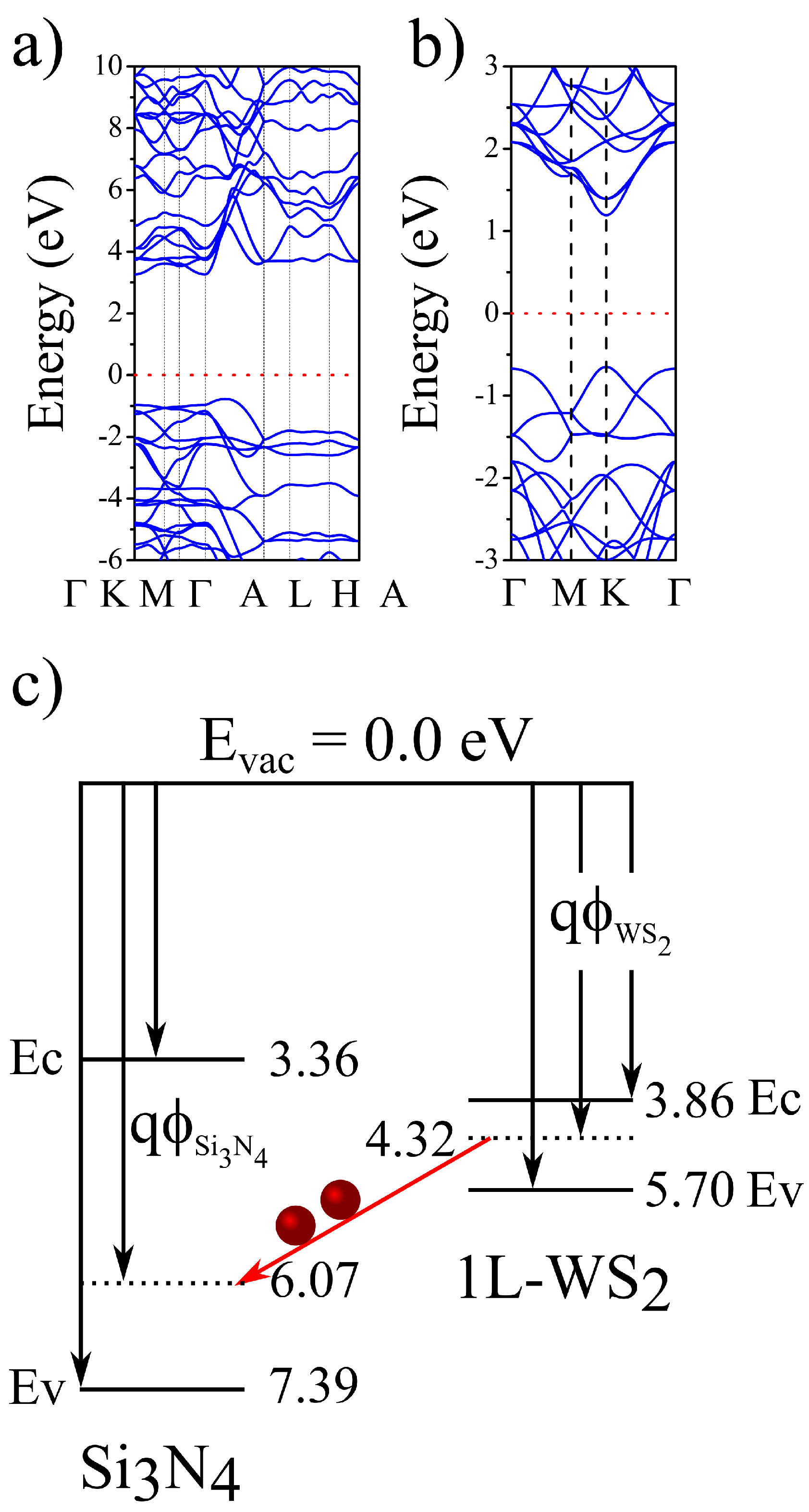
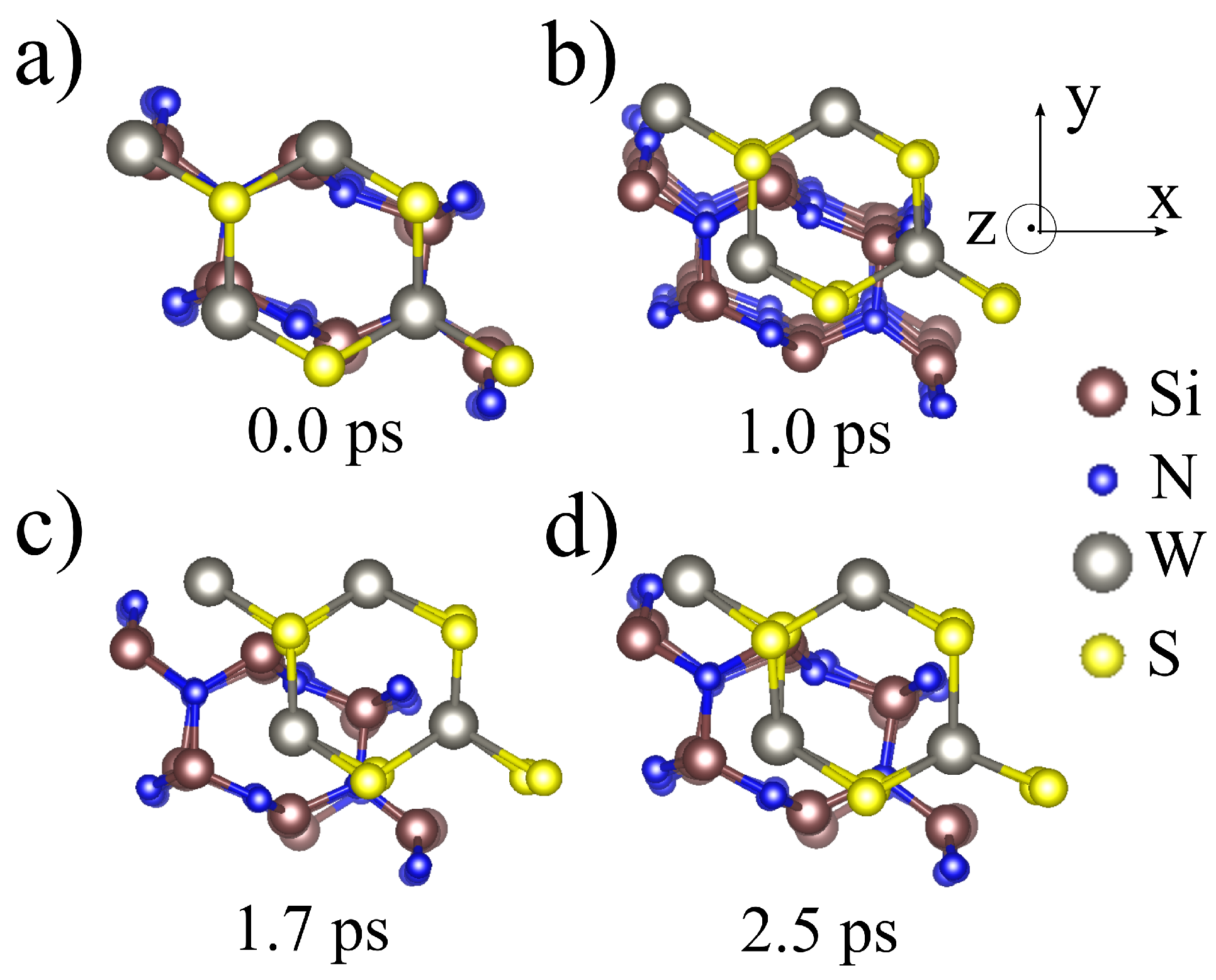
3. Results and Discussion
4. Conclusions
Supplementary Materials
Author Contributions
Funding
Institutional Review Board Statement
Informed Consent Statement
Data Availability Statement
Acknowledgments
Conflicts of Interest
References
- Wang, Q.H.; Kalantar-Zadeh, K.; Kis, A.; Coleman, J.N.; Strano, M.S. Electronics and optoelectronics of two-dimensional transition metal dichalcogenides. Nat. Nanotechnol. 2012, 7, 699–712. [Google Scholar] [CrossRef] [PubMed]
- Chhowalla, M.; Shin, H.S.; Eda, G.; Li, L.J.; Loh, K.P.; Zhang, H. The chemistry of two-dimensional layered transition metal dichalcogenide nanosheets. Nat. Chem. 2013, 5, 263–275. [Google Scholar] [CrossRef] [PubMed]
- Perea-López, N.; Elías, A.L.; Berkdemir, A.; Castro-Beltran, A.; Gutiérrez, H.R.; Feng, S.; Lv, R.; Hayashi, T.; López-Urías, F.; Ghosh, S.; et al. Photosensor Device Based on Few-Layered WS2 Films. Adv. Funct. Mater. 2013, 23, 5511–5517. [Google Scholar] [CrossRef]
- Bernardi, M.; Palummo, M.; Grossman, J.C. Extraordinary Sunlight Absorption and One Nanometer Thick Photovoltaics Using Two-Dimensional Monolayer Materials. Nano Lett. 2013, 13, 3664–3670. [Google Scholar] [CrossRef]
- Jariwala, D.; Sangwan, V.K.; Lauhon, L.J.; Marks, T.J.; Hersam, M.C. Emerging Device Applications for Semiconducting Two-Dimensional Transition Metal Dichalcogenides. ACS Nano 2014, 8, 1102–1120. [Google Scholar] [CrossRef] [PubMed]
- Son, Y.; Li, M.Y.; Cheng, C.C.; Wei, K.H.; Liu, P.; Wang, Q.H.; Li, L.J.; Strano, M.S. Observation of Switchable Photoresponse of a Monolayer WSe2–MoS2 Lateral Heterostructure via Photocurrent Spectral Atomic Force Microscopic Imaging. Nano Lett. 2016, 16, 3571–3577. [Google Scholar] [CrossRef]
- Cong, C.; Shang, J.; Wang, Y.; Yu, T. Optical Properties of 2D Semiconductor WS2. Adv. Opt. Mater. 2018, 6, 1700767. [Google Scholar] [CrossRef]
- Peimyoo, N.; Shang, J.; Cong, C.; Shen, X.; Wu, X.; Yeow, E.K.L.; Yu, T. Nonblinking, Intense Two-Dimensional Light Emitter: Monolayer WS2 Triangles. ACS Nano 2013, 7, 10985–10994. [Google Scholar] [CrossRef]
- Wang, Y.; Cong, C.; Yang, W.; Shang, J.; Peimyoo, N.; Chen, Y.; Kang, J.; Wang, J.; Huang, W.; Yu, T. Strain-induced direct–indirect bandgap transition and phonon modulation in monolayer WS2. Nano Res. 2015, 8, 2562–2572. [Google Scholar] [CrossRef]
- Cao, Q.; Dai, Y.W.; Xu, J.; Chen, L.; Zhu, H.; Sun, Q.Q.; Zhang, D.W. Realizing Stable p-Type Transporting in Two-Dimensional WS2 Films. ACS Appl. Mater. Interfaces 2017, 9, 18215–18221. [Google Scholar] [CrossRef]
- Eftekhari, A. Tungsten dichalcogenides (WS2, WSe2, and WTe2): Materials chemistry and applications. J. Mater. Chem. A 2017, 5, 18299–18325. [Google Scholar] [CrossRef]
- Wu, S.; Buckley, S.; Schaibley, J.R.; Feng, L.; Yan, J.; Mandrus, D.G.; Hatami, F.; Yao, W.; Vucković, J.; Majumdar, A.; et al. Monolayer semiconductor nanocavity lasers with ultralow thresholds. Nature 2015, 520, 69–72. [Google Scholar] [CrossRef] [PubMed]
- Ye, Y.; Wong, Z.J.; Lu, X.; Ni, X.; Zhu, H.; Chen, X.; Wang, Y.; Zhang, X. Monolayer excitonic laser. Nat. Photonics 2015, 9, 733–737. [Google Scholar] [CrossRef]
- Shang, J.; Cong, C.; Wang, Z.; Peimyoo, N.; Wu, L.; Zou, C.; Chen, Y.; Chin, X.Y.; Wang, J.; Soci, C.; et al. Room-temperature 2D semiconductor activated vertical-cavity surface-emitting lasers. Nat. Commun. 2017, 8, 543. [Google Scholar] [CrossRef]
- Kim, G.; Kim, H.M.; Kumar, P.; Rahaman, M.; Stevens, C.E.; Jeon, J.; Jo, K.; Kim, K.H.; Trainor, N.; Zhu, H.; et al. High-Density, Localized Quantum Emitters in Strained 2D Semiconductors. ACS Nano 2022, 16, 9651–9659. [Google Scholar] [CrossRef] [PubMed]
- Li, S.; Wang, S.; Tang, D.M.; Zhao, W.; Xu, H.; Chu, L.; Bando, Y.; Golberg, D.; Eda, G. Halide-assisted atmospheric pressure growth of large WSe2 and WS2 monolayer crystals. Appl. Mater. Today 2015, 1, 60–66. [Google Scholar] [CrossRef]
- Hohenberg, P.; Kohn, W. Inhomogeneous Electron Gas. Phys. Rev. 1964, 136, B864–B871. [Google Scholar] [CrossRef]
- Kohn, W.; Sham, L.J. Self-Consistent Equations Including Exchange and Correlation Effects. Phys. Rev. 1965, 140, A1133–A1138. [Google Scholar] [CrossRef]
- Soler, J.M.; Artacho, E.; Gale, J.D.; García, A.; Junquera, J.; Ordejón, P.; Sánchez-Portal, D. The SIESTA method for ab initio order-N materials simulation. J. Phys. Condens. Matter 2002, 14, 2745. [Google Scholar] [CrossRef]
- Junquera, J.; Paz, O.; Sánchez-Portal, D.; Artacho, E. Numerical atomic orbitals for linear-scaling calculations. Phys. Rev. B 2001, 64, 235111. [Google Scholar] [CrossRef]
- Perdew, J.P.; Burke, K.; Ernzerhof, M. Generalized Gradient Approximation Made Simple. Phys. Rev. Lett. 1996, 77, 3865–3868. [Google Scholar] [CrossRef] [PubMed]
- Troullier, N.; Martins, J.L. Efficient pseudopotentials for plane-wave calculations. Phys. Rev. B 1991, 43, 1993. [Google Scholar] [CrossRef] [PubMed]
- Monkhorst, H.J.; Pack, J.D. Special points for Brillouin-zone integrations. Phys. Rev. B 1976, 13, 5188–5192. [Google Scholar] [CrossRef]
- Nosé, S. A unified formulation of the constant temperature molecular dynamics methods. J. Chem. Phys. 1984, 81, 511. [Google Scholar] [CrossRef]
- Zhang, X.; Qiao, X.F.; Shi, W.; Wu, J.B.; Jiang, D.S.; Tan, P.H. Phonon and Raman scattering of two-dimensional transition metal dichalcogenides from monolayer, multilayer to bulk material. Chem. Soc. Rev. 2015, 44, 2757–2785. [Google Scholar] [CrossRef]
- Terrones, H.; Corro, E.D.; Feng, S.; Poumirol, J.M.; Rhodes, D.; Smirnov, D.; Pradhan, N.R.; Lin, Z.; Nguyen, M.A.T.; Elías, A.L.; et al. New First Order Raman-active Modes in Few Layered Transition Metal Dichalcogenides. Sci. Rep. 2014, 4, 4215. [Google Scholar] [CrossRef]
- Berkdemir, A.; Gutiérrez, H.R.; Botello-Méndez, A.R.; Perea-López, N.; Elías, A.L.; Chia, C.I.; Wang, B.; Crespi, V.H.; López-Urías, F.; Charlier, J.C.; et al. Identification of individual and few layers of WS2 using Raman Spectroscopy. Sci. Rep. 2013, 3, 1755. [Google Scholar] [CrossRef]
- Gutiérrez, H.R.; Perea-López, N.; Elías, A.L.; Berkdemir, A.; Wang, B.; Lv, R.; López-Urías, F.; Crespi, V.H.; Terrones, H.; Terrones, M. Extraordinary Room-Temperature Photoluminescence in Triangular WS2 Monolayers. Nano Lett. 2013, 13, 3447–3454. [Google Scholar] [CrossRef]
- Zhao, W.; Ghorannevis, Z.; Amara, K.K.; Pang, J.R.; Toh, M.; Zhang, X.; Kloc, C.; Tan, P.H.; Eda, G. Lattice dynamics in mono- and few-layer sheets of WS2 and WSe2. Nanoscale 2013, 5, 9677–9683. [Google Scholar] [CrossRef]
- Wang, F.; Li, S.; Bissett, M.A.; Kinloch, I.A.; Li, Z.; Young, R.J. Strain engineering in monolayer WS2 and WS2 nanocomposites. 2D Mater. 2020, 7, 045022. [Google Scholar] [CrossRef]
- Plechinger, G.; Nagler, P.; Kraus, J.; Paradiso, N.; Strunk, C.; Schüller, C.; Korn, T. Identification of excitons, trions and biexcitons in single-layer WS2. Phys. Status Solidi (RRL)—Rapid Res. Lett. 2015, 9, 457–461. [Google Scholar] [CrossRef]
- Dadgar, A.M.; Scullion, D.; Kang, K.; Esposito, D.; Yang, E.H.; Herman, I.P.; Pimenta, M.A.; Santos, E.J.G.; Pasupathy, A.N. Strain Engineering and Raman Spectroscopy of Monolayer Transition Metal Dichalcogenides. Chem. Mater. 2018, 30, 5148–5155. [Google Scholar] [CrossRef]
- Soignard, E.; Somayazulu, M.; Dong, J.; Sankey, O.F.; McMillan, P.F. High pressure-high temperature synthesis and elasticity of the cubic nitride spinel γ-Si3N4. J. Phys. Condens. Matter 2001, 13, 557–563. [Google Scholar] [CrossRef]
- Yeheskel, O.; Gefen, Y. The effect of the a phase on the elastic properties of Si3N4. Mater. Sci. Eng. 1985, 71, 95–99. [Google Scholar] [CrossRef]
- Singh, P.; Harbola, M.K.; Johnson, D.D. Better band gaps for wide-gap semiconductors from a locally corrected exchange-correlation potential that nearly eliminates self-interaction errors. J. Phys. Condens. Matter 2017, 29, 424001. [Google Scholar] [CrossRef] [PubMed]
- Terrones, H.; López-Urías, F.; Terrones, M. Novel hetero-layered materials with tunable direct band gaps by sandwiching different metal disulfides and diselenides. Sci. Rep. 2013, 3, 1549. [Google Scholar] [CrossRef]
- Britnell, L.; Ribeiro, R.M.; Eckmann, A.; Jalil, R.; Belle, B.D.; Mishchenko, A.; Kim, Y.J.; Gorbachev, R.V.; Georgiou, T.; Morozov, S.V.; et al. Strong Light-Matter Interactions in Heterostructures of Atomically Thin Films. Science 2013, 340, 1311–1314. [Google Scholar] [CrossRef]
- Cappelluti, E.; Roldán, R.; Silva-Guillén, J.A.; Ordejón, P.; Guinea, F. Tight-binding model and direct-gap/indirect-gap transition in single-layer and multilayer MoS2. Phys. Rev. B 2013, 88, 075409. [Google Scholar] [CrossRef]
- Nayak, A.P.; Yuan, Z.; Cao, B.; Liu, J.; Wu, J.; Moran, S.T.; Li, T.; Akinwande, D.; Jin, C.; Lin, J.F. Pressure-Modulated Conductivity, Carrier Density, and Mobility of Multilayered Tungsten Disulfide. ACS Nano 2015, 9, 9117–9123. [Google Scholar] [CrossRef]
- Cruz-Silva, E.; Lopez-Urias, F.; Munoz-Sandoval, E.; Sumpter, B.G.; Terrones, H.; Charlier, J.C.; Meunier, V.; Terrones, M. Phosphorus and phosphorus-nitrogen doped carbon nanotubes for ultrasensitive and selective molecular detection. Nanoscale 2011, 3, 1008–1013. [Google Scholar] [CrossRef]


| Paper | 2LA(M) | A | Type |
|---|---|---|---|
| This work | 350.6 | 418.7 | triangle |
| Gutiérres et al. [28] | - | 417.5 | triangle |
| Peymioo et al. [8] | 350.0 | 417.0 | triangle |
| Zhao et al. [29] | - | 418.0 | flake |
| Berkdemir et al. [27] | 352 | 417.5 | triangle |
| Terrones et al. [26] | - | 418.7 | unit cell 1 |
Disclaimer/Publisher’s Note: The statements, opinions and data contained in all publications are solely those of the individual author(s) and contributor(s) and not of MDPI and/or the editor(s). MDPI and/or the editor(s) disclaim responsibility for any injury to people or property resulting from any ideas, methods, instructions or products referred to in the content. |
© 2023 by the authors. Licensee MDPI, Basel, Switzerland. This article is an open access article distributed under the terms and conditions of the Creative Commons Attribution (CC BY) license (https://creativecommons.org/licenses/by/4.0/).
Share and Cite
Araujo, F.D.V.; Silva, F.W.N.; Zhang, T.; Zhou, C.; Lin, Z.; Perea-Lopez, N.; Rodrigues, S.F.; Terrones, M.; Souza Filho, A.G.; Alencar, R.S.; et al. Substrate-Induced Changes on the Optical Properties of Single-Layer WS2. Materials 2023, 16, 2591. https://doi.org/10.3390/ma16072591
Araujo FDV, Silva FWN, Zhang T, Zhou C, Lin Z, Perea-Lopez N, Rodrigues SF, Terrones M, Souza Filho AG, Alencar RS, et al. Substrate-Induced Changes on the Optical Properties of Single-Layer WS2. Materials. 2023; 16(7):2591. https://doi.org/10.3390/ma16072591
Chicago/Turabian StyleAraujo, F. D. V., F. W. N. Silva, T. Zhang, C. Zhou, Zhong Lin, Nestor Perea-Lopez, Samuel F. Rodrigues, Mauricio Terrones, Antônio Gomes Souza Filho, R. S. Alencar, and et al. 2023. "Substrate-Induced Changes on the Optical Properties of Single-Layer WS2" Materials 16, no. 7: 2591. https://doi.org/10.3390/ma16072591
APA StyleAraujo, F. D. V., Silva, F. W. N., Zhang, T., Zhou, C., Lin, Z., Perea-Lopez, N., Rodrigues, S. F., Terrones, M., Souza Filho, A. G., Alencar, R. S., & Viana, B. C. (2023). Substrate-Induced Changes on the Optical Properties of Single-Layer WS2. Materials, 16(7), 2591. https://doi.org/10.3390/ma16072591