Article

Analog Resistive Switching and Artificial Synaptic Behavior of ITO/WOX/TaN Memristors

1
Division of Electronics and Electrical Engineering, Dongguk University, Seoul 04620, Republic of Korea
2
Department of Electronics Engineering, Korea National University of Transportation, Chungju-si 27469, Republic of Korea
*
Authors to whom correspondence should be addressed.
Materials 2023, 16(4), 1687; https://doi.org/10.3390/ma16041687
Submission received: 25 November 2022 / Revised: 4 February 2023 / Accepted: 13 February 2023 / Published: 17 February 2023

Abstract

:
In this work, we fabricated an ITO/WOX/TaN memristor device by reactive sputtering to investigate resistive switching and conduct analog resistive switching to implement artificial synaptic devices. The device showed good pulse endurance (104 cycles), a high on/off ratio (>10), and long retention (>104 s) at room temperature. The conduction mechanism could be explained by Schottky emission conduction. Further, the resistive switching characteristics were performed by additional pulse-signal-based experiments for more practical operation. Lastly, the potentiation/depression characteristics were examined for 10 cycles. The results thus indicate that the WOX-based devices are appropriate candidates for synaptic devices as well as next-generation nonvolatile memory.

1. Introduction

Nonvolatile memory (NVM) devices with high switching speeds and high-density integration should be developed for the effective implementation of artificial intelligence (AI) technologies [1]. Because of the low cost and high compatibility of flash memory for complementary metal-oxide-semiconductor (CMOS) fabrication, silicon-based flash memories are the current market leaders for NVMs [2]. However, owing to physical limitations, we have reached the limit for increasing the memory density [3]. Accordingly, several candidates have emerged as replacements for traditional memory for NVM devices, including the ferroelectric field-effect transistor (FeFET) [4,5], phase-change memory (PCM) [6], magnetic random-access memory (MRAM) [7], and resistive random-access memory (RRAM) [8]. Among these emerging memories, RRAM has shown great potential for its advantages, such as fast and low power switching, high endurance, multilevel characteristics, applicability to flexible memory [9], and a high on/off ratio [10,11,12,13,14]; moreover, it has excellent scalability owing to its simple metal–insulator–metal (MIM) structure [15]. This scalability property of RRAM is one of the many reasons it has been widely studied for high-density cross-point arrays [16] and three-dimensional vertical RRAM (3D VRRAM) [17]. In addition, RRAM devices can be used as artificial synaptic devices for neuromorphic computing because of the advantages described above [18,19,20,21]. Neuromorphic systems are emerging as alternatives to the Von Neumann structure, which is the existing computing method, because it has reached its limit due to bottlenecks [22]. Neuromorphic computing mimics the behavior of the human brain [23] and requires an artificial cell that acts as a synapse, for which the RRAM cell may be an appropriate candidate [18].
Digital information is stored in the form of binary numbers “0” or “1”. In the case of RRAM, the stored information is determined to be “0” or “1” based on the resistance state [24], where the low-resistance state (LRS) corresponds to “1” and the high-resistance state (HRS) corresponds to “0”. RRAM devices are usually in the HRS initially [25]. To switch the device from the initial state, a procedure called “forming” is required; forming refers to the application of high-voltage stress that causes a soft breakdown in the insulator layer. In addition, a compliance current (CC) should be applied to protect the switching layer from permanent breakdown when applying the forming voltage [26]. After changing to the LRS, a “reset” procedure that applies a voltage of opposite polarity to the “forming” voltage is required to return to the HRS. To switch to LRS from HRS again, a “set” procedure is needed; the “set” process involves applying a voltage of opposite polarity to the “reset” voltage. The range of current flow between the LRS and HRS as well as the voltage range required for “set” and “reset” vary from one device to another [25]; hence, these can be used as criteria to evaluate the power consumption of an RRAM device [27].
Presently, researchers are investigating suitable materials to realize more ideal RRAM characteristics. Resistive switching has been observed in transition-metal oxides (TMO), such as zinc, tantalum, and tungsten oxides [28,29,30]. In particular, tungsten oxide is a compatible material with CMOS technology [31], making it easier to integrate RRAM into the existing back-end-of-line Si technologies. Each TMO used in the switching layer exhibits various characteristics. However, the type of TMO used affects the switching characteristics of the device, in addition to the composition ratio of the metal oxide and the number of oxygen vacancies within a given material [32]. Resistance switching in TMO systems is often based on the formation and rupture of the conductive filament (CF) that usually comprises oxygen vacancies [33]. The composition ratio of a TMO can be varied by changing the gas flow rate ratio of oxygen (O2) and argon (Ar) during sputtering [34]. Moreover, the cost and commercial availability should be considered when choosing materials for the RRAM. In addition, if indium tin oxide (ITO) is selected as an electrode, the device can be employed in light-based applications, such as transparent memory [35], photodetectors [36], and displays, owing to its transparency [37].
In this study, we investigate WOX-based memristor devices in which the tungsten oxide as the switching layer is deposited by reactive sputtering.
Electrical experiments are then conducted to characterize the resistive switching of the device. Furthermore, the device is tested for its applicability in the pulsed operation mode and as an artificial synaptic device in neuromorphic engineering.

2. Materials and Methods

2.1. Preparation Method

The fabrication process of the ITO/WOX/TaN RRAM device is as follows: First, a 100 nm TaN bottom electrode (BE) layer was deposited on a SiO2/Si substrate by direct current (DC) sputtering using a Ta target (99.95% purity) in a mixture of Ar and N2 gases. Then, a ~25 nm WOX thin-film insulator was deposited as a switching layer by radio frequency (RF) sputtering using a W target (99.95% purity) in a mixture of Ar and O2. The WOX layer was deposited with an O2-gas flow rate of 66.7% {O2/(Ar + O2) = 20 sccm/(10 + 20) sccm}. Finally, a 100 nm thick ITO top electrode (TE), which was deposited by RF sputtering using an ITO target (99.99% purity) in Ar gas, was defined by a mask aligner process for a cell size of 100 μm × 100 μm.

2.2. Test and Characterization

The cross-sectional view and film thickness of the ITO/WOX/TaN structure was confirmed using a transmission electron microscope (TEM, KANC, Suwon, Republic of Korea) with focused ion beam (FIB) milling. The electrical characteristics and pulse measurement of the devices were obtained using a semiconductor parameter analyzer (Keithley 4200-SCS and PMU ultrafast mode, Tektronix Inc., Beaverton, OR, USA); an external bias evoked from the analyzer module was applied to all ITO TE devices with the TaN BE being grounded.

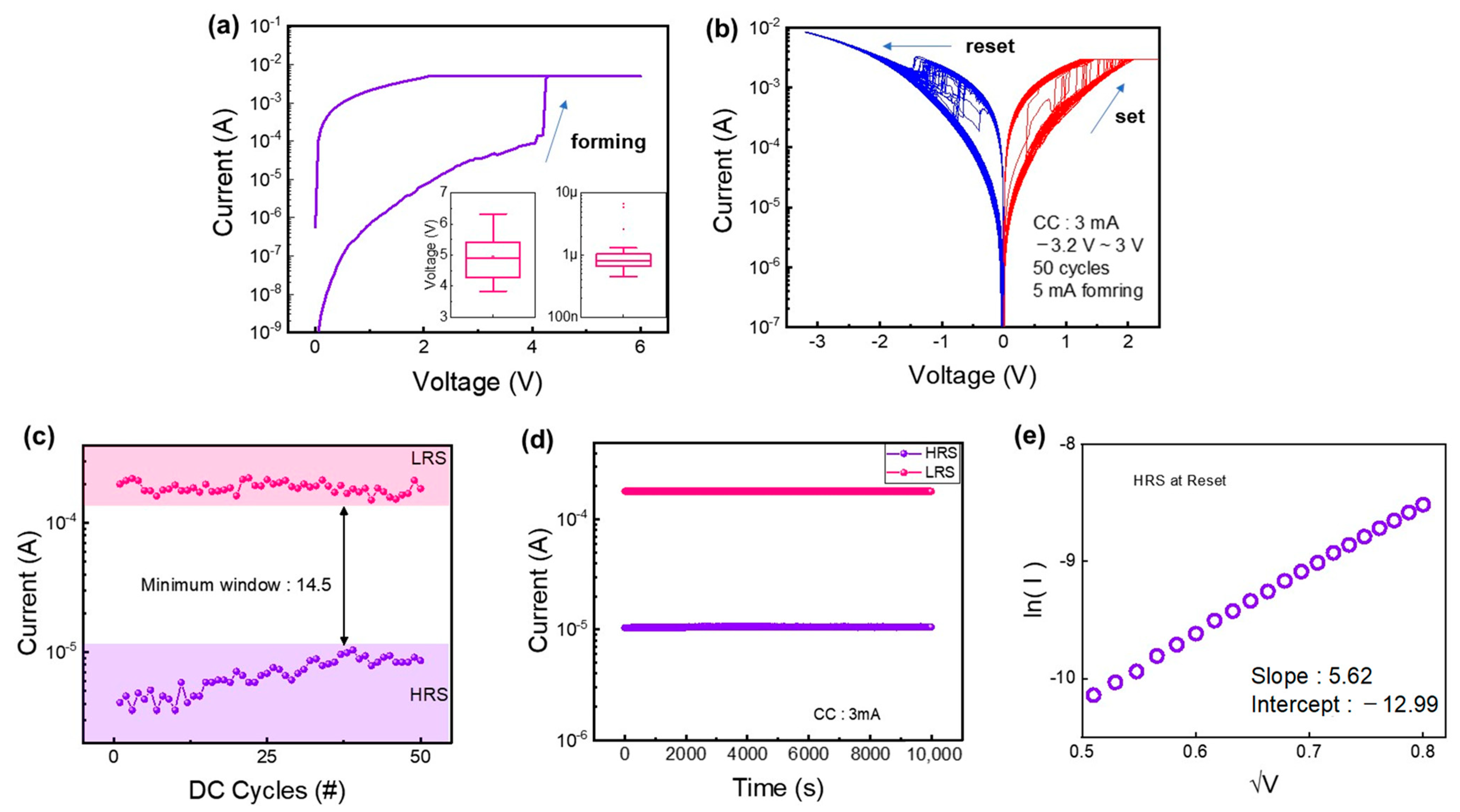
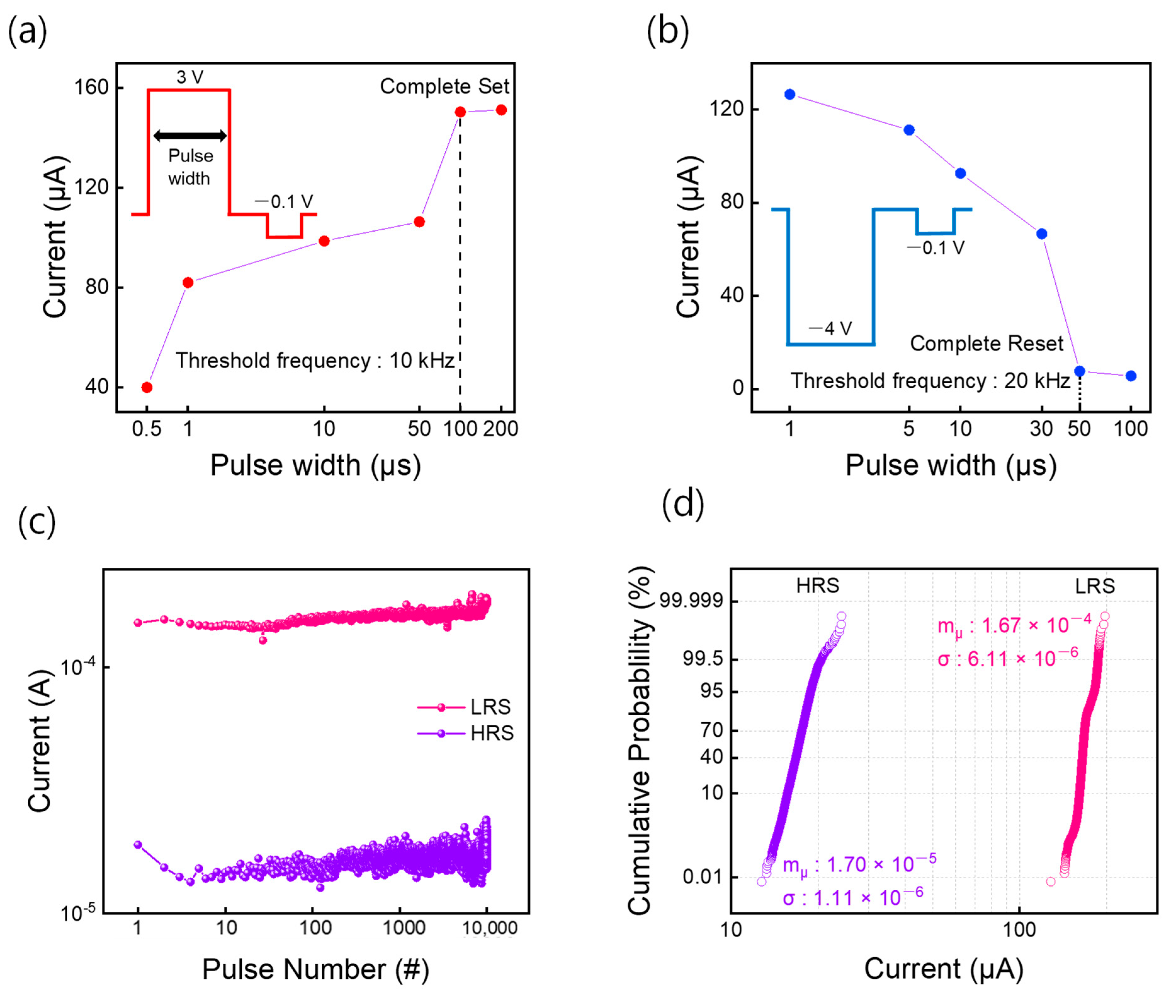
3. Results and Discussion

Figure 1a shows the schematic of the structure of the ITO/WOX/TaN device. A probe tip used to apply the external voltage was placed in contact with the ITO TE, and another probe tip for grounding was placed in contact with the TaN BE. We confirmed the presence of the main layers of the device from the cross-sectional TEM image and SEM image. Figure 1b shows the top-view SEM image of the device. Figure 1c is a cross-sectional SEM image of an area without ITO TE. As shown in Figure 1d, a WOX layer of about 25 nm thickness was deposited between the upper ITO and lower TaN layers; the layers are separated by the yellow dotted lines.
The chemical state of the WOX bulk layer was investigated by X-ray photoelectron spectroscopy (XPS). Figure 2a,b shows the XPS spectrum of W 4f and O 1s, respectively. The binding energy of the pink dotted line at 38.21 eV (W 4f5/2) and 36.29 eV (W 4f7/2) corresponds to the W6+ oxidation state. Likewise, the green and pink doublets correspond to the W5+ oxidation state and the W4+ oxidation state, respectively. The spectrum of O 1s has doublet peaks, of which one is oxygen deficiency (532.08 eV) and the other is W-O bonding (531.21 eV) [35].
The electrical properties of the device are described below. First, the forming curve is shown in Figure 3a. The forming voltage was 4.91 V from the measurement of 45 cells and the initial current at the reading of 1 V was 779 nA from 30 cells. It is noted that the initial current was quite high because the sputtering deposited WOX film had a lot of oxygen vacancies. Figure 3b shows the I–V characteristics of the device after the forming process. The DC sweep of 50 cycles was conducted under the same CC (3 mA) and voltage range (−3.2 V to 2.5 V) to achieve repetitive counterclockwise bipolar resistive switching. The current of the device increased when the positive bias was applied for a set process. Conversely, the current decreased with negative bias for a reset process. The possible switching mechanism of the device was the change of the TaON layer [38]. TaN was initially easily oxidized with the WOX layer. The TaON layer was reduced as the oxygen vacancies in WOX migrated to the TaON layer with a positive bias. In other words, as the thickness of TaON decreased, the conductance of the entire memristor system increased. Conversely, the conductance decreased with a negative bias as the TaON layer became thicker.
To investigate the conduction mechanism based on the barrier height modulation of the TaON layer, the I–V curve of the device in the HRS was fitted and interpreted based on the Schottky emission conduction mechanism. Figure 3e shows the fitting plots and Schottky slope values. The result of Schottky current fitting was linear. This indicates that carrier transport was dominated by Schottky emission [39]. Equation (1) is used for the Schottky emission conduction:
J = A * T 2 e x p [ q ( B q E 4 π ε i d ) k T ]
where  A *  is the effective Richardson constant,  T  is the Kelvin temperature,  B  is the Schottky barrier height,  ε i  is the dielectric constant,  k  is the Boltzmann constant, and  d  is the Schottky barrier distance which is the switching gap of the RRAM.  J  is the current density and it can be expressed as  I A A  is the effective RRAM area, which is the cross-sectional area perpendicular to the direction in which the current flows. To evaluate the  l n ( I T 2 )  vs.  V  fitting curve, the Schottky emission conduction formula was transformed into the following equation:
l n ( I T 2 ) = q q E 4 π ε i d k T V q B k T + l n A A *
This equation can be considered a linear function of  V  and  l n ( I T 2 ) . Therefore, we plotted the I–V curves with the x-axis as  V  and Y axis as  l n ( I T 2 ) ; here,  q q E 4 π ε i d k T  is the slope of the linear function, and  q B k T + l n A *  is the intercept. Since the other parameters except  B  in the intercept are constants, the intercept can be said to be proportional to  B . Hence, an increase in the intercept indicates a decrease in the Schottky barrier height, which indicates a decrease in the dielectric. Meanwhile, since the other parameters except for  1 ε i d  in the slope are constants, the slope is considered proportional to  1 ε i d . Thus, if the dielectric decreases, the slope should increase.
Figure 3c shows the DC endurances of the devices at a read voltage of −0.1 V. In addition, it is possible to obtain the on/off ratios related to the read margin, which is one of the important characteristics of a memory device [40]. The minimum on/off ratio is calculated by dividing the minimum value among the currents in the LRS by the maximum value among the currents in the HRS. The devices showed no significant decay during 50 repetitions of the DC sweep but had different minimum on/off ratios. The results of the retention test are shown in Figure 3d. The retention test was conducted for 104 s at a reading voltage of −0.1 V at room temperature after experiencing 100 switching cycles. The device did not experience serious degradations under the time conditions.
Additional pulse measurements were performed on the devices to demonstrate the practical operation of the device. For the pulse-switching endurance test, the optimal pulse condition to switch the device was used, as shown in Figure 4a,b. For the same voltage amplitudes (set: 3 V, reset: −4 V), we observed the points at which a complete set or reset occurred. Further, the shortest pulse width that can achieve complete switching (set: 100 μs, reset: 50 μs) was chosen to improve the speed of operation. Pulse endurance tests of 104 cycles were conducted under the pulse conditions in Figure 4c. The device suffered no severe read/write disturbances after more than 104 cycles. For further analysis, the pulse-switching data were compiled into a cumulative probability plot, as shown in Figure 4d. The mean and standard deviation of the current distributions for the HRS and LRS are given in Figure 4d.
Finally, we demonstrated 10 cycles of potentiation and depression, as illustrated in Figure 5. The positive pulse amplitude was tuned to 1.25 V and the negative one was tuned to −1.40 V, while the pulse width was set to 1 ms. The read voltage was −0.1 V, which was small enough to not disturb operation. One cycle consisted of 50 identical set pulses followed by a sequence of 50 identical reset pulses. The device showed good reproducibility for 10 cycles. The confirmation of the potentiation and depression characteristics proves that the device can be applied to neuromorphic and artificial synaptic devices. Table 1 illustrates the comparison of electrical parameters and synaptic properties of existing WOX-based memristors.

4. Conclusions

In conclusion, the WOX-based RRAM device successfully mimicked biological synaptic functions for use in neuromorphic computing. Through some important electrical tests, it was determined that all the devices showed stable switching endurances for 50 cycles and lengthy retention above 104 s. Additionally, the device endured 104 switching cycles well with pulsed signals. The potentiation/depression characteristics of the device, which suggests its similarity to the neurotransmitters in biological synapses, were also evaluated. Taking the exploratory results into consideration, we believe that the RRAM device structure proposed in this study is a promising avenue for future research on NVM and neuromorphic devices.

Author Contributions

Conceptualization, Y.C. and S.K.; writing—original draft preparation, Y.C.; writing—review and editing, J.K., M.K. and S.K.; supervision, S.K.; Funding acquisition, M.K. All authors have read and agreed to the published version of the manuscript.

Funding

This research was supported by National R&D Program through the National Research Foundation of Korea (NRF) funded by the Ministry of Science and ICT (2021M3F3A2A03017693) and was supported by Basic Science Research Program through the National Research Foundation of Korea (NRF) funded by the Ministry of Education (2018R1A6A1A03023788).

Institutional Review Board Statement

Not applicable.

Informed Consent Statement

Not applicable.

Data Availability Statement

Not applicable.

Conflicts of Interest

The authors declare no conflict of interest.

References

  1. Hung, J.M.; Li, X.; Wu, J.; Chang, M.F. Challenges and trends in developing nonvolatile memory-enabled computing chips for intelligent edge devices. IEEE Trans. Electron Devices 2020, 67, 1444–1453. [Google Scholar] [CrossRef]
  2. Kim, S.; Yong, S.; Kim, W.; Kang, S.; Park, H.; Yoon, K.; Sheen, D.; Lee, S.; Hwang, C. Review of semiconductor flash memory devices for material and process issues. Adv. Mater. 2022, 2022, 2200659. [Google Scholar] [CrossRef] [PubMed]
  3. Lee, G.; Hwang, S.; Yu, J.; Kim, H. Architecture and process integration overview of 3D NAND flash technologies. Appl. Sci. 2021, 11, 6703. [Google Scholar] [CrossRef]
  4. Luo, Z.-D.; Zhang, S.; Liu, Y.; Zhang, D.; Gan, X.; Seidel, J.; Liu, Y.; Han, G.; Alexe, M.; Hao, Y. Dual-Ferroelectric-Coupling-Engineered Two-Dimensional Transistors for Multifunctional In-Memory Computing. ACS Nano 2022, 16, 3362–3372. [Google Scholar] [CrossRef]
  5. Khan, A.I.; Keshavarzi, A.; Datta, S. The future of ferroelectric field-effect transistor technology. Nat. Electron. 2020, 3, 588–597. [Google Scholar] [CrossRef]
  6. Burr, G.W. Phase change memory technology. J. Vac. Sci. Technol. B 2010, 25, 223. [Google Scholar] [CrossRef] [Green Version]
  7. Ishdorj, B.; Kim, J.; Kim, J.H.; Na, T. A Timing-Based Split-Path Sensing Circuit for STT-MRAM. Micromachines 2022, 13, 1004. [Google Scholar] [CrossRef]
  8. Kwon, O.; Lee, Y.; Kang, M.; Kim, S. Synaptic plasticity features and neuromorphic system simulation in AlN-based memristor devices. J. Alloy. Compd. 2022, 911, 164870. [Google Scholar] [CrossRef]
  9. Dastgeer, G.; Afzal, A.M.; Aziz, J.; Hussain, S.; Jaffery, S.H.A.; Kim, D.; Imran, M.; Assiri, M.A. Flexible Memory Device Composed of Metal-Oxide and Two-Dimensional material (SnO2/WTe2) Exhibiting Stable Resistive Switching. Materials 2021, 14, 7535. [Google Scholar] [CrossRef]
  10. Huang, C.H.; Huang, J.S.; Lai, C.C.; Huang, H.W.; Lin, S.J.; Chueh, Y.L. Manipulated Transformation of Filamentary and Homogeneous Resistive Switching on ZnO Thin Film Memristor with Controllable Multistate. ACS Appl. Mater. Interfaces 2013, 5, 6017–6023. [Google Scholar] [CrossRef]
  11. Lee, S.H.; Zhu, X.; Lu, W.D. Nanoscale resistive switching devices for memory and computing applications. Nano Res. 2020, 13, 1228–1243. [Google Scholar] [CrossRef]
  12. Pan, C.H.; Chang, T.C.; Tsai, T.M.; Chang, K.C.; Chu, T.J.; Lin, W.Y.; Chen, M.C.; Sze, S.M. Confirmation of filament dissolution behavior by analyzing electrical field effect during reset process in oxide-based RRAM. Appl. Phys. Lett. 2016, 109, 133503. [Google Scholar] [CrossRef]
  13. Lee, S.R.; Kim, Y.B.; Chang, M.; Kim, K.M.; Lee, C.B.; Hur, J.H.; Park, G.S.; Lee, D.; Lee, M.J.; Kim, C.J.; et al. Multi-level switching of triple-layered TaOx RRAM with excellent reliability for storage class memory. In Proceedings of the 2012 Symposium on VLSI Technology (VLSIT), Honolulu, HI, USA, 12–14 June 2012; IEEE: Piscataway, NJ, USA, 2012; pp. 71–72. [Google Scholar] [CrossRef]
  14. Ielmini, D. Brain-inspired computing with resistive switching memory (RRAM): Devices, synapses and neural networks. Microelectron. Eng. 2018, 190, 44–53. [Google Scholar] [CrossRef]
  15. Prakash, A.; Jana, D.; Maikap, S. TaOx -based resistive switching memories: Prospective and challenges. Nanoscale Res. Lett. 2013, 8, 1–17. [Google Scholar] [CrossRef] [Green Version]
  16. Xia, L.; Gu, P.; Li, B.; Tang, T.; Yin, X.; Huangfu, W.; Yu, S.; Cao, Y.; Wang, Y.; Yang, H. Technological Exploration of RRAM Crossbar Array for Matrix-Vector Multiplication. J. Comput. Sci. Technol. 2016, 31, 3–19. [Google Scholar] [CrossRef]
  17. Zhang, L.; Cosemans, S.; Wouters, D.J.; Govereanu, B.; Groeseneken, G.; Jurczak, M. Analysis of vertical cross-point resistive memory (VRRAM) for 3D RRAM design. In Proceedings of the 2013 5th IEEE International Memory Workshop, Monterey, CA, USA, 26–29 May 2013; IEEE: Piscataway, NJ, USA, 2013; pp. 155–158. [Google Scholar] [CrossRef]
  18. Hong, X.L.; Loy, D.J.J.; Dananjaya, P.A.; Tan, F.; Ng, C.M.; Lew, W.S. Oxide-based RRAM materials for neuromorphic computing. J. Mater. Sci. 2018, 53, 8720–8746. [Google Scholar] [CrossRef]
  19. Sun, J.; Han, G.; Zeng, Z.; Wang, Y. Memristor-Based Neural Network Circuit of Full-Function Pavlov Associative Memory With Time Delay and Variable Learning Rate. IEEE Trans. Cybern. 2019, 50, 2935–2945. [Google Scholar] [CrossRef]
  20. Sun, J.; Wang, Y.; Liu, P.; Wen, S.; Wang, Y. Memristor-Based Neural Network Circuit With Multimode Generalization and Differentiation on Pavlov Associative Memory. IEEE Trans. Cybern. 2022, 1–12. [Google Scholar] [CrossRef]
  21. Ding, S.; Wang, N.; Bao, H.; Chen, B.; Wu, H.; Xu, Q. Memristor synapse-coupled piecewise-linear simplified Hopfield neural network: Dynamics analysis and circuit implementation. Chaos Solition Fract. 2023, 166, 112899. [Google Scholar] [CrossRef]
  22. Zokaee, F.; Zarandi, H.R.; Jiang, L.; Aligne, R. A Process-in-Memory Architecture for Short Read Alignment in ReRAMs. IEEE Comput. Archit. Lett. 2018, 17, 237–240. [Google Scholar] [CrossRef]
  23. Upadhyay, N.K.; Jiang, H.; Asapu, S.; Xia, Q.; Joshua, Y.J. Emerging Memory Devices for Neuromorphic Computing. Adv. Mater. Technol. 2019, 4, 1800589. [Google Scholar] [CrossRef] [Green Version]
  24. Giacomin, E.; Greenberg-Toledo, T.; Kvatinsky, S.; Gaillardon, P.E. A Robust Digital RRAM-Based Convolutional Block for Low-Power Image Processing and Learning Applications. IEEE Trans. Circuits Syst. I Regul. Pap. 2018, 66, 643–654. [Google Scholar] [CrossRef]
  25. Sawa, A. Resistive switching in transition metal oxides. Mater. Today 2008, 11, 28–36. [Google Scholar] [CrossRef]
  26. Sun, C.; Lu, S.M.; Jin, F.; Mo, W.Q.; Song, J.L.; Dong, K.F. The Resistive Switching Characteristics of TiN/HfO2/Ag RRAM Devices with Bidirectional Current Compliance. J. Electron. Mater. 2019, 48, 2992–2999. [Google Scholar] [CrossRef]
  27. Cheng, C.H.; Chin, A.; Yeh, F.S. Novel Ultra-low power RRAM with good endurance and retention. In Proceedings of the 2010 Symposium on VLSI Technology, Honolulu, Hawaii, 14–17 June 2010; IEEE: Piscataway, NJ, USA, 2010; pp. 85–86. [Google Scholar]
  28. Simanjunak, F.M.; Panda, D.; Wei, K.H.; Tseng, T.Y. Status and Prospects of ZnO-Based Resistive Switching Memory Devices. Nanoscale Res. Lett. 2016, 11, 368. [Google Scholar] [CrossRef] [Green Version]
  29. Wu, W.T.; Wu, J.J.; Chen, J.S. Resistive Switching Behavior and Multiple Transmittance States in Solution-Processed Tungsten Oxide. ACS Appl. Mater. Interfaces 2011, 3, 2616–2621. [Google Scholar] [CrossRef]
  30. Chein, W.C.; Chen, Y.C.; Chang, K.P.; Lai, E.K.; Yao, Y.D.; Lin, P.; Gong, J.; Tsai, S.C.; Hsieh, S.H.; Chen, C.F.; et al. Multi-Level Operation of Fully CMOS Compatible WOX Resistive Random Access Memory (RRAM). In Proceedings of the 2009 IEEE International Memory Workshop, Monterey, CA, USA, 10–14 May 2009; IEEE: Piscataway, NJ, USA, 2009; pp. 1–2. [Google Scholar] [CrossRef]
  31. Tsai, T.M.; Tan, Y.F.; Wu, C.H.; Yang, C.C.; Chen, W.C.; Lin, C.C.; Wu, P.Y.; Zhang, Y.C.; Chou, S.Y.; Chen, Z.Y.; et al. Impact of oxygen flow rate on performance of indium-tin-oxide-based RRAMs. J. Phys. Appl. Phys. 2021, 54, 295103. [Google Scholar] [CrossRef]
  32. Wang, H.; Yan, X. Overview of Resistive Random Access Memory (RRAM): Materials, Filament Mechanisms, Performance Optimization, and Prospects. Phys. Status Solidi RRL 2019, 13, 1900073. [Google Scholar] [CrossRef]
  33. Petzold, S.; Piros, E.; Eihardt, R.; Zintler, A.; Vogel, T.; Kaiser, N.; Radetinac, A.; Komissinskiy, P.; Jalaguier, E.; Nolot, E.; et al. Tailoring the Switching Dynamics in Yttrium Oxide-Based RRAM Devices by Oxygen Engineering: From Digital to Multi-Level Quantization toward Analog Switching. Adv. Electron. Mater. 2020, 6, 2000439. [Google Scholar] [CrossRef]
  34. Lien, S.Y. Characterization and optimization of ITO thin films for application in heterojunction silicon solar cells. Thin Solid Films 2010, 518, S10–S13. [Google Scholar] [CrossRef]
  35. Kim, J.; Park, J.; Kim, S. Bipolar Switching Characteristics of Transparent WOX-Based RRAM for Synaptic Application and Neuromorphic Engineering. Materials 2022, 15, 7185. [Google Scholar] [CrossRef]
  36. Kim, S.I.; Cho, S.H.; Choi, S.R.; Oh, M.C.; Jang, J.H.; Song, P.K. Crystallization and electrical properties of ITO:Ce thin films for flat panel display applications. Thin Solid Films 2009, 517, 4061–4064. [Google Scholar] [CrossRef]
  37. Luo, Q.; Xu, X.; Liu, H.; Lv, H.; Gong, T.; Long, S.; Liu, Q.; Sun, H.; Banerjee, W.; Li, L.; et al. Demonstration of 3D vertical RRAM with ultra low-leakage, high-selectivity and self-compliance memory cells. In Proceedings of the 2015 IEEE International Electron Devices Meeting (IEDM), Washington, DC, USA, 7–9 December 2015; IEEE: Piscataway, NJ, USA, 2015; pp. 10.2.1–10.2.4. [Google Scholar] [CrossRef]
  38. Ismail, M.; Mahata, C.; Kim, S. Electronic synaptic plasticity and analog switching characteristics in Pt/TiOx/AlOx/AlTaON/TaN multilayer RRAM for artificial synapses. Appl. Sur. Sci. 2022, 599, 153906. [Google Scholar] [CrossRef]
  39. Hsieh, W.K.; Lam, K.T.; Chang, S.J. Bipolar Ni/ZnO/HfO2/Ni RRAM with multilevel characteristic by different reset bias. Mater. Sci. Semicond. Process. 2015, 35, 30–33. [Google Scholar] [CrossRef]
  40. Shang, D.S.; Shi, L.; Sun, J.R.; Shen, B.G.; Zhunge, F.; Li, R.W.; Zhao, Y.G. Improvement of reproducible resistance switching in polycrystalline tungsten oxide films by in situ oxygen annealing. Appl. Phys. Lett. 2010, 96, 072103. [Google Scholar] [CrossRef] [Green Version]
  41. Hsu, C.C.; Chuang, H.; Jhang, W.C. Annealing effect on forming-free bipolar resistive switching characteristics of sol-gel WOx resistive memories with Al conductive bridges. J. Alloys Compd. 2021, 882, 160758. [Google Scholar] [CrossRef]
  42. Lai, E.K.; Chien, W.C.; Chen, Y.C.; Hong, T.J.; Lin, Y.Y.; Chang, K.P.; Yao, Y.D.; Lin, P.; Horng, S.F.; Gong, J. Tungsten Oxide Resistive Memory Using Rapid Thermal Oxidation of Tungsten Plugs. J. Appl. Phys. 2010, 49, 04DD17. [Google Scholar] [CrossRef] [Green Version]
Figure 1. (a) Schematic illustration of the ITO/WOX/TaN device structure. (b) SEM image of the top electrode patterns. (c) SEM image of the WOX/TaN layers. (d) TEM image of ITO/WOx/TaN layers.
Materials 16 01687 g001
Figure 2. XPS spectra of the WOX switching layer. (a) Three different doublets of W 4f core level spectra. (b) O 1s core level spectra.
Materials 16 01687 g002
Figure 3. (a) Forming voltage statistics based on 45 cells of each of the devices and initial current statistics based on 30 cells before the forming process. (b) I–V curves in 50 cycles by DC sweep. (c) Endurance and (d) retention of the device. (e) In(I) versus V1/2 for typical I–V curve in HRS.
Materials 16 01687 g003
Figure 4. Pulse characteristics of Device #3. (a) Current values after applying a single set pulse for different pulse widths. (b) Current values after applying a single reset pulse for different pulse widths. (c) The pulse endurance test conducted with the optimal set pulse (3 V, 100 μs) and reset pulse (–4 V, 50 μs). (d) Cumulative probability obtained from the pulse endurance test.
Materials 16 01687 g004
Figure 5. Ten cycles of potentiation (pink) and depression (violet) of the device for 50 identical set pulses (1.25 V, 1 ms) followed by 50 identical reset pulses (−1.40 V, 1 ms) in each cycle.
Materials 16 01687 g005
Table 1. Comparison of WOX-based memristors from previous studies.
Device
Structure
ProcessForming Voltage
(V)
on/off
Ratio
Endurance
(#)
Retention
(s)
Synaptic
Properties
Ref.
Au/WO3/FTOPLD2.6102>104>104N/A[40]
Al/WOX/ITOSol-gelForming-free~103>102N/AN/A[41]
TiN/WOX/WRTO3.5>102>108N/AN/A[42]
Al/WOX/WPlasma oxidation410>40>106N/A[30]
ITO/WOX/ITOSputteringForming-free~5300>104Potentiation/
Depression
[35]
ITO/WOX/TaNSputtering4.91>10>104>104Potentiation/
Depression
(This work)
Disclaimer/Publisher’s Note: The statements, opinions and data contained in all publications are solely those of the individual author(s) and contributor(s) and not of MDPI and/or the editor(s). MDPI and/or the editor(s) disclaim responsibility for any injury to people or property resulting from any ideas, methods, instructions or products referred to in the content.

