
Application of Proton Irradiation in the Study of Accelerated Radiation Ageing in a GaAs Semiconductor
 , , , and
Abstract
1. Introduction
2. Experimental
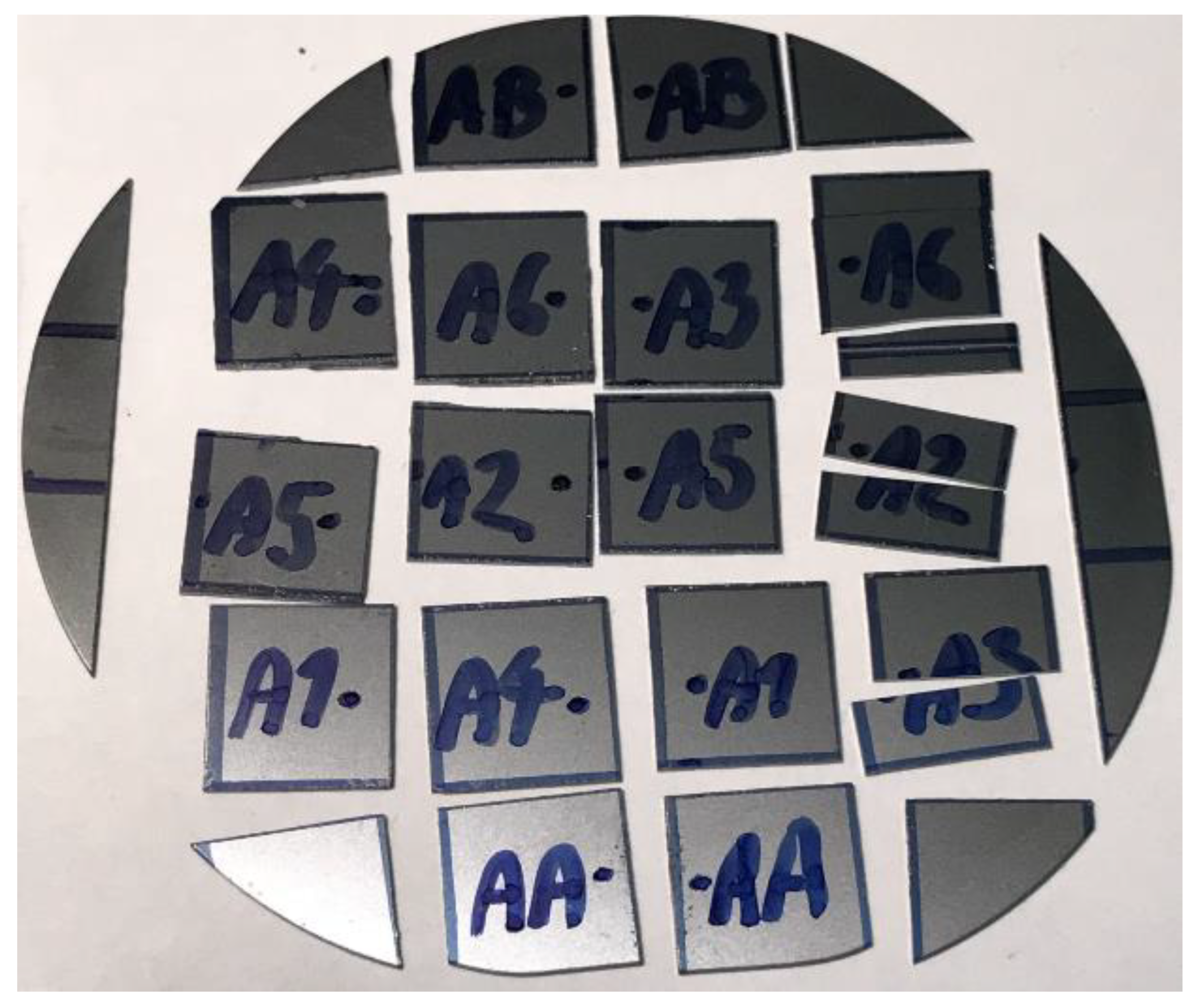
2.1. Material and Sample Preparation
2.2. Proton Irradiation Experiment
2.3. Positron Annihilation Spectroscopy Characterisation
3. Results and Discussion
4. Conclusions
- Positron annihilation spectroscopy can be effectively used as a tool for the quantitative characterisation of vacancy-type defects in semiconductors exposed to harsh radiation environments. While the present experiments led to a vacancy concentration near the saturation limit of PAS, the optimal proton fluence for future irradiation experiments can be selected from the range of 1015–1016 cm−2.
- The results indicate that mild radiation environments involving high-energy protons can be effectively simulated and accelerated by employing relatively high proton fluxes. Moreover, the proton irradiation seems to induce a concentration of vacancy-type defects (mono-vacancies) that is reasonably similar to high-energy electron irradiation experiments with a similar fluence.
- While SRIM code simulations provide data about the production rates of radiation-induced defects, the presented PAS characterisation enables reliable quantification of the survival rate of the defects. Similar to numerous studies in the past and referenced in this work, the presented experiment can be expanded to include the study of the recovery of the microstructure after thermal annealing of the samples.
- There is a threshold flux above which the proton irradiation experiment becomes unreasonable and inefficient. This threshold is relatively high and lies above 1012 s−1 cm−2. At a higher proton flux, the new displacement damage cascades are initiated while the previous cascades are still occurring. This results in a sharp reduction in the concertation of the surviving vacancies.
Author Contributions
Funding
Institutional Review Board Statement
Informed Consent Statement
Data Availability Statement
Conflicts of Interest
References
- Van Tuyl, R.L. The Early Days of GaAs Ics. In Proceedings of the 2010 IEEE Compound Semiconductor Integrated Circuit Symposium (CSICS), Monterey, CA, USA, 3–6 October 2010; pp. 1–4. [Google Scholar] [CrossRef]
- Pearton, S.J.; Aitkaliyeva, A.; Xian, M.; Ren, F.; Khachatrian, A.; Ildefonso, A.; Kim, J. Review—Radiation Damage in Wide and Ultra-Wide Bandgap Semiconductors. ECS J. Solid State Sci. Technol. 2021, 10, 055008. [Google Scholar] [CrossRef]
- Reed, K.; Goetz, C.; Ericson, N.; Sweeney, D.; Ezell, N.D. Wide Bandgap Semiconductors for Extreme Temperature and Radiation Environments; Oak Ridge National Lab: Oak Ridge, TN, USA, 2022. [Google Scholar] [CrossRef]
- Kizilyalli, I.C.; Xu, Y.A.; Carlson, E.; Manser, J.; Cunningham, D.W. Current and Future Directions in Power Electronic Devices and Circuits Based on Wide Band-Gap Semiconductors. In Proceedings of the 2017 IEEE 5th Workshop on Wide Bandgap Power Devices and Applications (WiPDA), Albuquerque, NM, USA, 30 October–1 November 2017; p. 417. [Google Scholar] [CrossRef]
- Huang, A.Q. Wide bandgap (WBG) Power Devices and their Impacts on Power Delivery Systems. In Proceedings of the 2016 IEEE International Electron Devices Meeting (IEDM), San Francisco, CA, USA, 3–7 December 2016; pp. 20.1.1–20.1.4. [Google Scholar] [CrossRef]
- Shenai, K. Future Prospects of Widebandgap (WBG) Semiconductor Power Switching Devices. IEEE Trans. Electron. Devices 2015, 62, 248–257. [Google Scholar] [CrossRef]
- Wide-Bandgap Semiconductors for Space Applications; Last Update: 15 February 2022. Record Number: 96633; European Union. 2022. Available online: https://cordis.europa.eu/project/id/242394 (accessed on 1 December 2022).
- Millán, J.; Godignon, P.; Perpiñà, X.; Pérez-Tomás, A.; Rebollo, J.A. Survey of Wide Bandgap Power Semiconductor Devices. IEEE Trans. Power Electron. 2014, 29, 2155–2163. [Google Scholar] [CrossRef]
- Maurer, R.H.; Fraeman, M.E.; Martin, M.N.; Roth, D.R. Harsh Environments: Space Radiation Environment, Effects, and Mitigation. John Hopkins APL Tech. Dig. 2008, 28, 17. [Google Scholar]
- Bourban, G. Radiation Environment and its Effects in EEE Components and Hardness Assurance for Space Applications. In Proceedings of the CERN-ESA-SSC workshop European Space Agency ESA, Zurich, Switzerland, 9–10 May 2017. [Google Scholar]
- Krstic, M. A Methodology for Characterization, Modeling and Mitigation of Single Event Transient Effects in CMOS Standard Combinational Cells. Doctoral Thesis, Postdam University, Postdam, Germany, April 2022. [Google Scholar] [CrossRef]
- Rafí, J.M.; Pellegrini, G.; Godignon, P.; Ugobono, S.O.; Rius, G.; Tsunoda, I.; Moll, M. Electron, Neutron, and Proton Irradiation Effects on SiC Radiation Detectors. IEEE Trans. Nucl. Sci. 2020, 67, 2481–2489. [Google Scholar] [CrossRef]
- Summers, G.P.; Burke, E.A.; Shapiro, S.R.; Walters, R.J. Damage correlations in semiconductors exposed to gamma, electron and proton radiations. IEEE Trans. Nucl. Sci. 1993, 40, 1372–1379. [Google Scholar] [CrossRef]
- Marshall, P.W.; Dale, C.J.; Summers, G.P.; Wolicki, E.A.; Burke, E.A. Proton, neutron, and electron-induced displacement damage in germanium. IEEE Trans. Nucl. Sci. 1989, 36, 1882–1888. Available online: https://www.osti.gov/biblio/7202239 (accessed on 13 December 2022). [CrossRef]
- Väyrynen, S. Irradiation of Silicon Particle Detectors with Mev-Protons; University of Helsinki Report Series in Physics: Helsinky, Finland, 2010; ISBN 978-952-10-5975-9. [Google Scholar]
- Advanced Technologies Research Institute. B8405—Specifications and Machine Logs for 6 MV Tandetron System; Internal document of the ATRI MTF STU; Advanced Technologies Research Institute: Tokyo, Japan, 2022. [Google Scholar]
- Noga, P.; Száraz, Z.; Kubiš, M.; Dobrovodský, J.; Ferenčík, F.; Riedlmajer, R.; Krsjak, V. High-Fluence Multi-Energy Ion Irradiation for Testing of Materials. Materials 2022, 15, 6443. [Google Scholar] [CrossRef] [PubMed]
- Norgett, M.J.; Robinson, M.T.; Torrens, I.M. A proposed method of calculating displacement dose rates. Nucl. Eng. Des. 1975, 33, 50. [Google Scholar] [CrossRef]
- Stoller, R.E. On the use of SRIM for computing radiation damage exposure. Nucl. Instrum. Methods Phys. Res. Sect. B: Beam Interact. Mater. At. Vol. 2013, 310, 75–80. [Google Scholar] [CrossRef]
- Allison, J.; Amako, K.; Apostolakis, J. Geant4 developments and applications. IEEE Trans. Nucl. Sci. 2006, 53, 270–278. [Google Scholar] [CrossRef]
- Giebel, G.; Kansy, J. LT10 Program for Solving Basic Problems Connected with Defect Detection. Phys. Procedia. 2012, 35, 122–127. [Google Scholar] [CrossRef]
- Rehberg, R.K.; Leipner, H.S. Positron Annihilation in Semiconductors; Springer Verlag: Berlin/Heidelberg, Germany, 1999; p. 378. [Google Scholar] [CrossRef]
- Krsjak, V.; Degmova, J.; Noga, P.; Petriska, M.; Sojak, S.; Saro, M.; Slugen, V. Application of Positron Annihilation Spectroscopy in Accelerator-Based Irradiation Experiments. Materials 2021, 14, 6238. [Google Scholar] [CrossRef] [PubMed]
- Sagatova, A.; Krsjak, V.; Sojak, S.; Riabukhin, O.; Kovacova, E.; Zatko, B. Semi-insulating GaAs detectors degraded by 8 MeV electrons up to 1500 kGy. J. Instrum. 2021, 16, C12032. [Google Scholar] [CrossRef]
- Ulbricht, A.; Hernández-Mayoral, M.; Oñorbe, E.; Etienne, A.; Radiguet, B.; Hirschmann, E.; Bergner, F. Effect of Neutron Flux on an Irradiation-Induced Microstructure and Hardening of Reactor Pressure Vessel Steels. Metals 2022, 12, 369. [Google Scholar] [CrossRef]


| Parameter | Properties |
|---|---|
| Product No. | 82045 |
| Method | GaAs LEC |
| Description | Monocrystalline wafers |
| Type | Semi-insulating, undoped |
| Dopant | N/A |
| Resistivity | 4.38 × 10⁸ Ohm cm |
| Hall Mobility | 5398 Cm2 V−1 s |
| Orientation | (100) ± 0.5° |
| Off Orientation | Off 2° towards (110)° |
| Diameter | 50.8 ± 0.1 mm |
| Thickness | 500 ± 25 μm |
| Surface | SSP |
| Front side | Polished |
| Back side | Lapped/etched |
| Sample Set No. | Irradiation Time [min]/[h] | Flux [cm−2.s−1] |
|---|---|---|
| Set 0 (reference) | 0/0 | 0 |
| Set 1 | 16/0.27 | 1.04 × 10¹³ |
| Set 2 | 36/0.59 | 4.63 × 10¹² |
| Set 3 | 222/3.70 | 7.51 × 10¹¹ |
| Set 4 | 505/8.42 | 3.30 × 10¹¹ |
| Set 5 | 1599/26.65 | 1.04 × 10¹¹ |
| GaAs Samples | p+ Flux [cm−2] | t1 [ps] | I1 [%] | t2 [ps] | I2 [%] | tAVG [ps] | FV | kV [s−1] | NV [cm−3] |
|---|---|---|---|---|---|---|---|---|---|
| Set 1 | 1.04 × 10¹³ | 223 | 98.98% | 295 | 1.02% | 223.7 | 0.97 | 9.27 × 10⁶ | 4.64 × 10¹⁴ |
| Set 2 | 4.63 × 10¹² | 221 | 85.00% | 295 | 15.00% | 231.8 | 0.93 | 1.58 × 10⁸ | 7.92 × 10¹⁵ |
| Set 3 | 7.51 × 10¹¹ | 215 | 50.00% | 295 | 50.00% | 254.0 | 1.05 | 8.97 × 10⁸ | 4.49 × 10¹⁶ |
| Set 4 | 3.30 × 10¹¹ | 210 | 50.00% | 295 | 50.00% | 251.5 | 0.99 | 8.97 × 10⁸ | 4.49 × 10¹⁶ |
| Set 5 | 1.04 × 10¹¹ | 203 | 46.00% | 295 | 54.00% | 251.6 | 1.07 | 1.05 × 10⁹ | 5.27 × 10¹⁶ |
Disclaimer/Publisher’s Note: The statements, opinions and data contained in all publications are solely those of the individual author(s) and contributor(s) and not of MDPI and/or the editor(s). MDPI and/or the editor(s) disclaim responsibility for any injury to people or property resulting from any ideas, methods, instructions or products referred to in the content. |
© 2023 by the authors. Licensee MDPI, Basel, Switzerland. This article is an open access article distributed under the terms and conditions of the Creative Commons Attribution (CC BY) license (https://creativecommons.org/licenses/by/4.0/).
Share and Cite
Neuhold, I.; Noga, P.; Sojak, S.; Petriska, M.; Degmova, J.; Slugen, V.; Krsjak, V. Application of Proton Irradiation in the Study of Accelerated Radiation Ageing in a GaAs Semiconductor. Materials 2023, 16, 1089. https://doi.org/10.3390/ma16031089
Neuhold I, Noga P, Sojak S, Petriska M, Degmova J, Slugen V, Krsjak V. Application of Proton Irradiation in the Study of Accelerated Radiation Ageing in a GaAs Semiconductor. Materials. 2023; 16(3):1089. https://doi.org/10.3390/ma16031089
Chicago/Turabian StyleNeuhold, Igor, Pavol Noga, Stanislav Sojak, Martin Petriska, Jarmila Degmova, Vladimir Slugen, and Vladimir Krsjak. 2023. "Application of Proton Irradiation in the Study of Accelerated Radiation Ageing in a GaAs Semiconductor" Materials 16, no. 3: 1089. https://doi.org/10.3390/ma16031089
APA StyleNeuhold, I., Noga, P., Sojak, S., Petriska, M., Degmova, J., Slugen, V., & Krsjak, V. (2023). Application of Proton Irradiation in the Study of Accelerated Radiation Ageing in a GaAs Semiconductor. Materials, 16(3), 1089. https://doi.org/10.3390/ma16031089