
Lead-Free Halide Perovskite Nanocrystals for Light-Emitting Diodes


Abstract
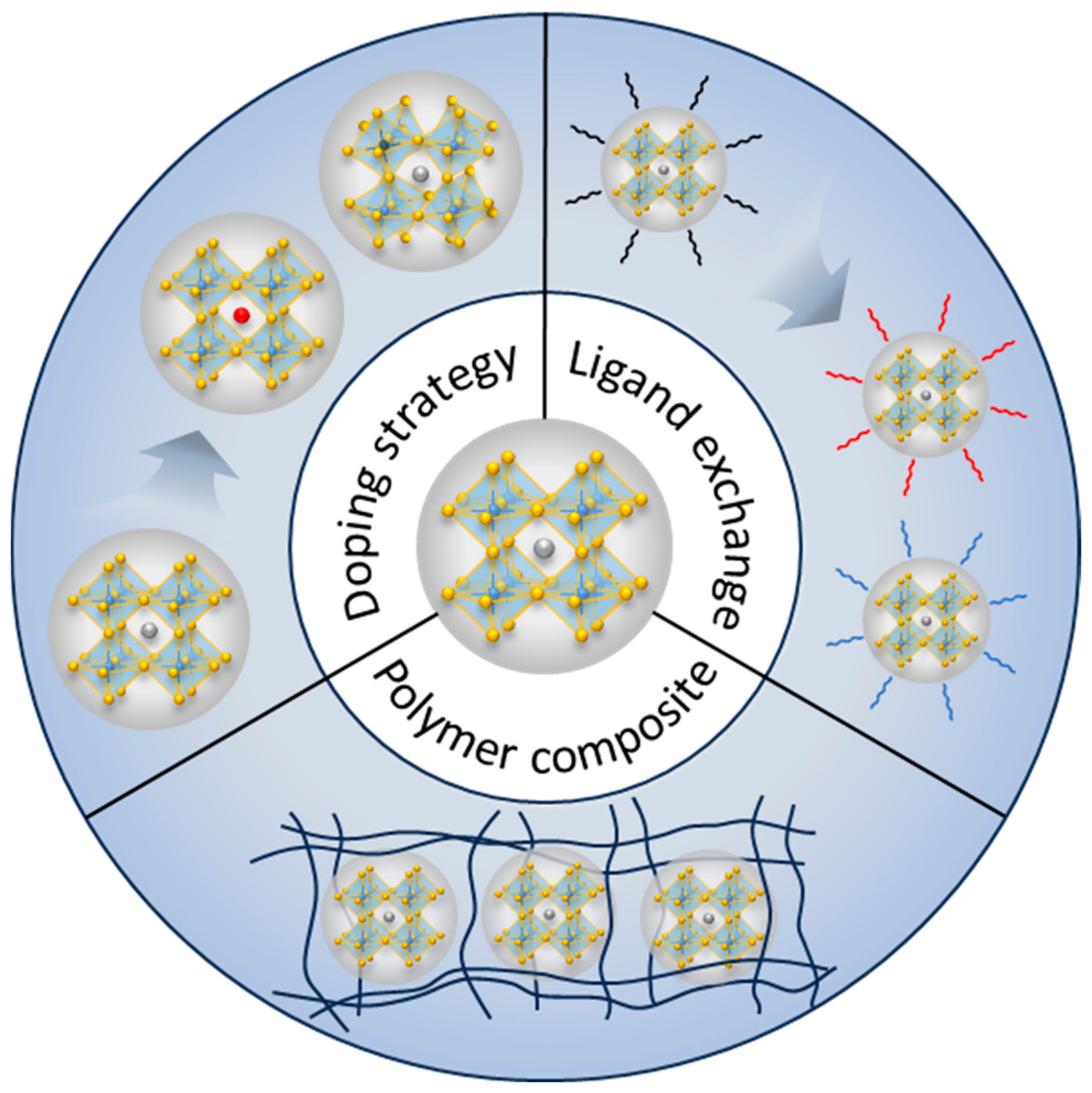
:1. Introduction
2. B-Site Metal Candidates for Pb-Free Perovskite Nanocrystals
2.1. Sn-Based Perovskite Nanocrystals

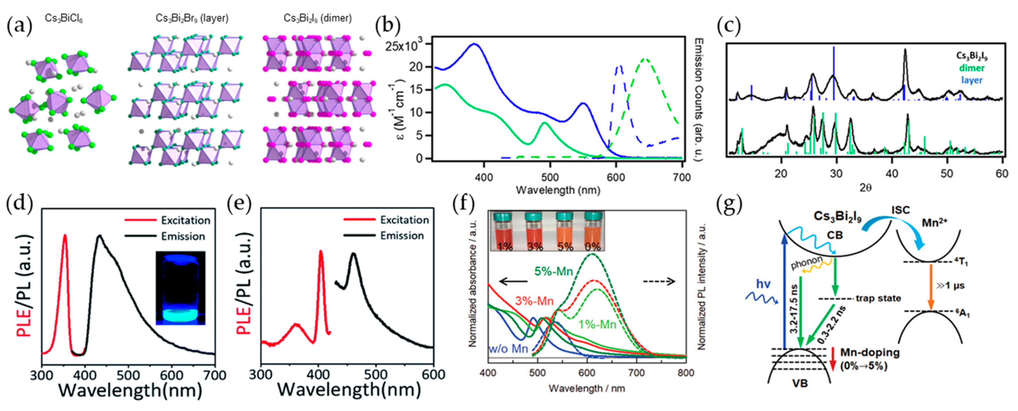
2.2. Bi-Based Perovskite Nanocrystals
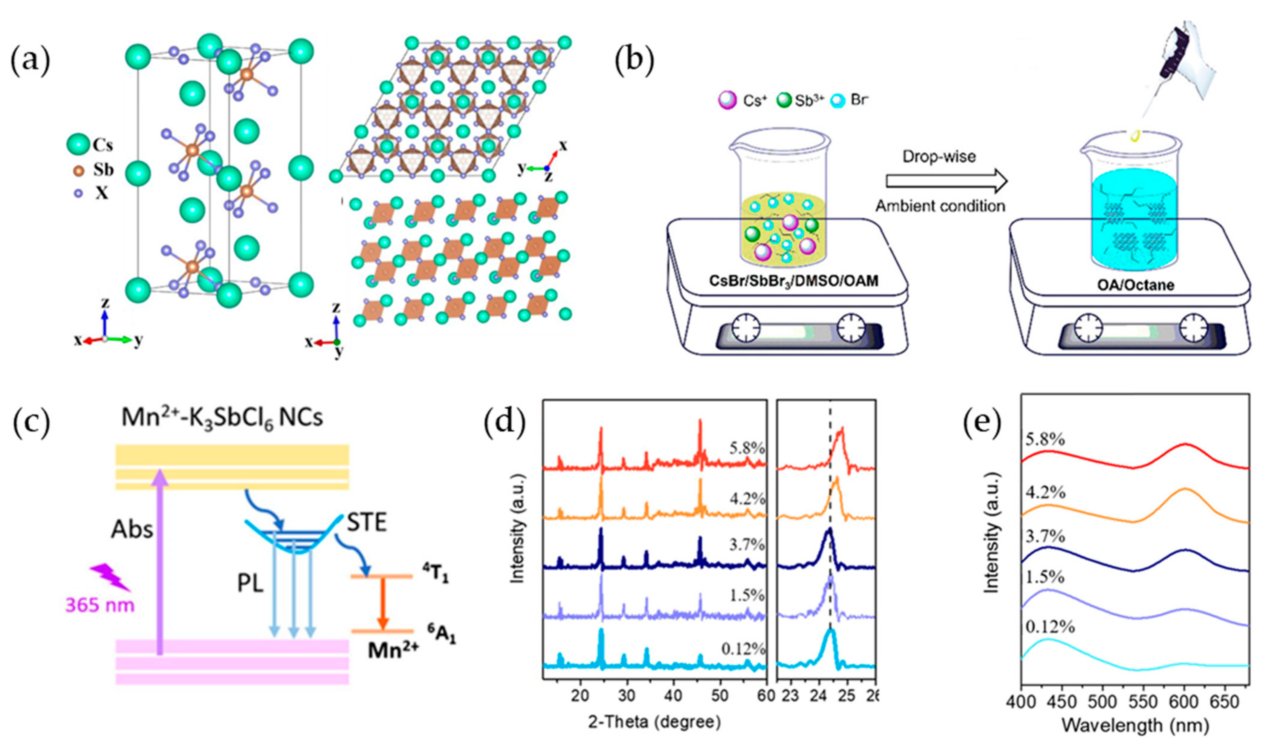
2.3. Sb-Based Perovskite Nanocrystals
2.4. Cu-Based Perovskite Nanocrystals

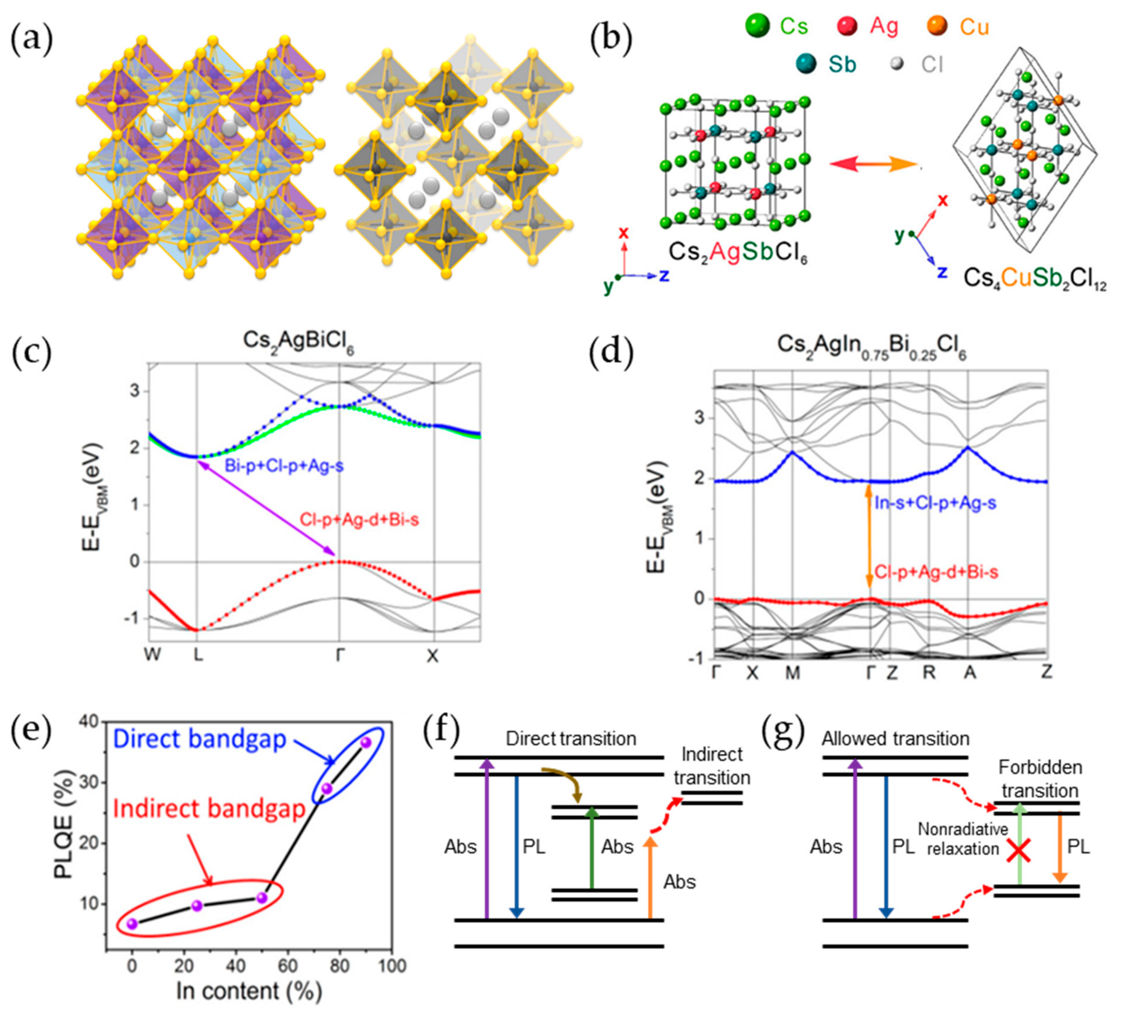
2.5. Double Perovskite Nanocrystals

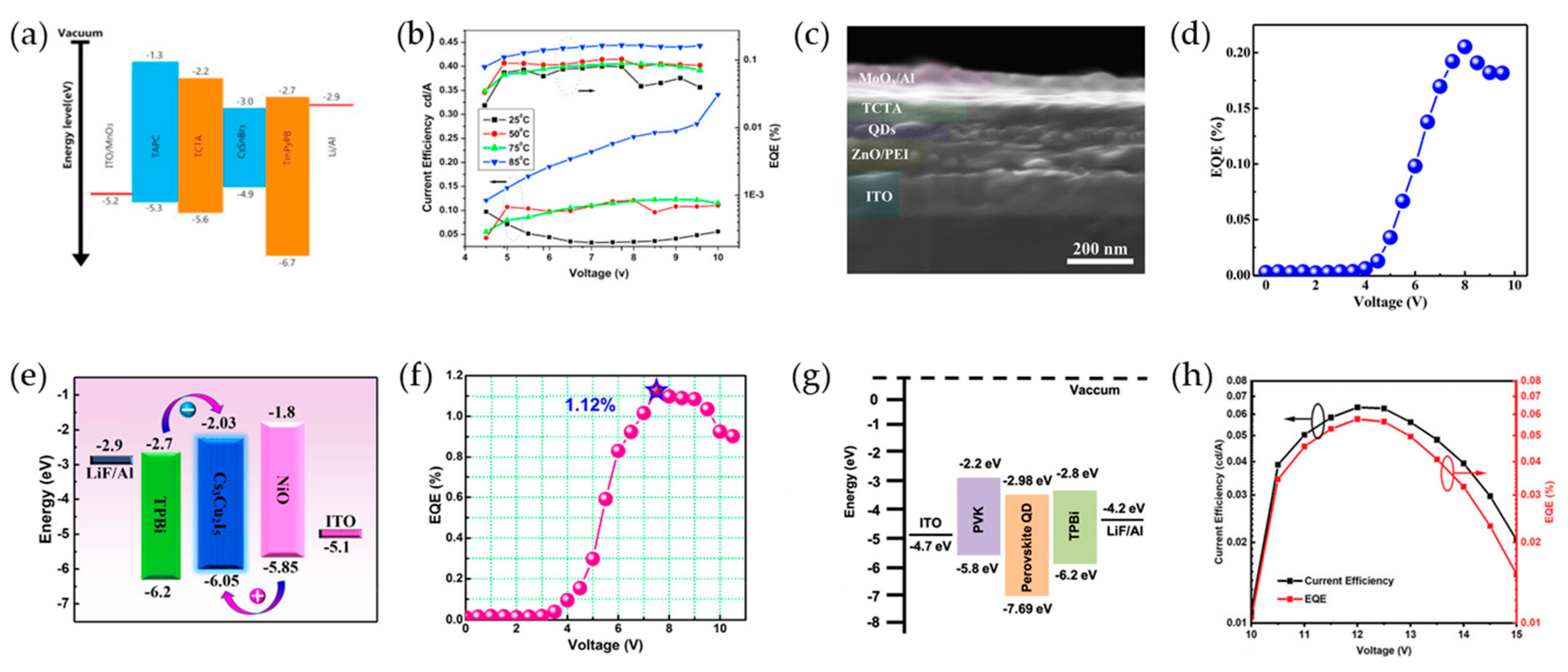
3. Pb-Free Perovskite Nanocrystal-Based LEDs
4. Conclusions
Author Contributions
Funding
Institutional Review Board Statement
Informed Consent Statement
Data Availability Statement
Conflicts of Interest
References
- Stranks, S.D.; Snaith, H.J. Metal-Halide Perovskites for Photovoltaic and Light-Emitting Devices. Nat. Nanotechnol. 2015, 10, 391–402. [Google Scholar] [CrossRef] [PubMed]
- Xiao, Z.; Kerner, R.A.; Zhao, L.; Tran, N.L.; Lee, K.M.; Koh, T.-W.; Scholes, G.D.; Rand, B.P. Efficient Perovskite Light-Emitting Diodes Featuring Nanometre-Sized Crystallites. Nat. Photonics 2017, 11, 108–115. [Google Scholar] [CrossRef]
- Liu, X.K.; Xu, W.; Bai, S.; Jin, Y.; Wang, J.; Friend, R.H.; Gao, F. Metal Halide Perovskites for Light-Emitting Diodes. Nat. Mater. 2021, 20, 10–21. [Google Scholar] [CrossRef]
- Park, M.H. 3D and 2D Metal Halide Perovskites for Blue Light-Emitting Diodes. Materials 2022, 15, 4571. [Google Scholar] [CrossRef] [PubMed]
- Lee, M.M.; Teuscher, J.; Miyasaka, T.; Murakami, T.N.; Snaith, H.J. Efficient Hybrid Solar Cells Based on Meso-Superstructured Organometal Halide Perovskites. Science 2012, 338, 643–647. [Google Scholar] [CrossRef]
- Burschka, J.; Pellet, N.; Moon, S.-J.; Humphry-Baker, R.; Gao, P.; Nazeeruddin, M.K.; Grätzel, M. Sequential Deposition as a Route to High-Performance Perovskite-Sensitized Solar Cells. Nature 2013, 499, 316–319. [Google Scholar] [CrossRef] [PubMed]
- Ono, L.K.; Qi, Y.; Liu, S.F. Progress toward Stable Lead Halide Perovskite Solar Cells. Joule 2018, 2, 1961–1990. [Google Scholar] [CrossRef]
- Yakunin, S.; Sytnyk, M.; Kriegner, D.; Shrestha, S.; Richter, M.; Matt, G.J.; Azimi, H.; Brabec, C.J.; Stangl, J.; Kovalenko, M.V.; et al. Detection of X-ray Photons by Solution-Processed Lead Halide Perovskites. Nat. Photonics 2015, 9, 444–449. [Google Scholar] [CrossRef]
- Tian, W.; Zhou, H.; Li, L. Hybrid Organic–Inorganic Perovskite Photodetectors. Small 2017, 13, 1702107. [Google Scholar] [CrossRef]
- Wang, Y.; Li, X.; Nalla, V.; Zeng, H.; Sun, H. Solution-Processed Low Threshold Vertical Cavity Surface Emitting Lasers from All-Inorganic Perovskite Nanocrystals. Adv. Funct. Mater. 2017, 27, 1605088. [Google Scholar] [CrossRef]
- Kanhere, P.; Chen, Z. A Review on Visible Light Active Perovskite-Based Photocatalysts. Molecules 2014, 19, 19995–20022. [Google Scholar] [CrossRef] [PubMed]
- Kim, T.H.; Park, I.; Lee, K.H.; Sim, J.H.; Park, M.H.; Han, T.H.; Paik, U.; Jang, J.; Park, H.B.; Kim, Y.H. Investigating the Interfacial Properties of Halide Perovskite/TiOx Heterostructures for Versatile Photocatalytic Reactions under Sunlight. Nanoscale 2023, 15, 7710–7714. [Google Scholar] [CrossRef] [PubMed]
- Liu, H.; Liu, Z.; Xu, W.; Yang, L.; Liu, Y.; Yao, D.; Zhang, D.; Zhang, H.; Yang, B. Engineering the Photoluminescence of CsPbX3 (X = Cl, Br, and I) Perovskite Nanocrystals Across the Full Visible Spectra with the Interval of 1 Nm. ACS Appl. Mater. Interfaces 2019, 11, 14256–14265. [Google Scholar] [CrossRef] [PubMed]
- Nedelcu, G.; Protesescu, L.; Yakunin, S.; Bodnarchuk, M.I.; Grotevent, M.J.; Kovalenko, M.V. Fast Anion-Exchange in Highly Luminescent Nanocrystals of Cesium Lead Halide Perovskites (CsPbX3, X = Cl, Br, I). Nano Lett. 2015, 15, 5635–5640. [Google Scholar] [CrossRef] [PubMed]
- Akkerman, Q.A.; Rainò, G.; Kovalenko, M.V.; Manna, L. Genesis, Challenges and Opportunities for Colloidal Lead Halide Perovskite Nanocrystals. Nat. Mater. 2018, 17, 394–405. [Google Scholar] [CrossRef] [PubMed]
- Huang, H.; Susha, A.S.; Kershaw, S.V.; Hung, T.F.; Rogach, A.L. Control of Emission Color of High Quantum Yield CH3NH3PbBr3 Perovskite Quantum Dots by Precipitation Temperature. Adv. Sci. 2015, 2, 1500194. [Google Scholar] [CrossRef]
- Mir, W.J.; Warankar, A.; Acharya, A.; Das, S.; Mandal, P.; Nag, A. Colloidal Thallium Halide Nanocrystals with Reasonable Luminescence, Carrier Mobility and Diffusion Length. Chem. Sci. 2017, 8, 4602–4611. [Google Scholar] [CrossRef]
- Huang, H.; Bodnarchuk, M.I.; Kershaw, S.V.; Kovalenko, M.V.; Rogach, A.L. Lead Halide Perovskite Nanocrystals in the Research Spotlight: Stability and Defect Tolerance. ACS Energy Lett. 2017, 2, 2071–2083. [Google Scholar] [CrossRef]
- Protesescu, L.; Yakunin, S.; Bodnarchuk, M.I.; Krieg, F.; Caputo, R.; Hendon, C.H.; Yang, R.X.; Walsh, A.; Kovalenko, M.V. Nanocrystals of Cesium Lead Halide Perovskites (CsPbX3, X = Cl, Br, and I): Novel Optoelectronic Materials Showing Bright Emission with Wide Color Gamut. Nano Lett. 2015, 15, 3692–3696. [Google Scholar] [CrossRef]
- Kovalenko, M.V.; Protesescu, L.; Bodnarchuk, M.I. Properties and Potential Optoelectronic Applications of Lead Halide Perovskite Nanocrystals. Science 2017, 358, 745–750. [Google Scholar] [CrossRef]
- Talapin, D.V.; Lee, J.S.; Kovalenko, M.V.; Shevchenko, E.V. Prospects of Colloidal Nanocrystals for Electronic and Optoelectronic Applications. Chem. Rev. 2010, 110, 389–458. [Google Scholar] [CrossRef] [PubMed]
- Kambhampati, P. Multiexcitons in Semiconductor Nanocrystals: A Platform for Optoelectronics at High Carrier Concentration. J. Phys. Chem. Lett. 2012, 3, 1182–1190. [Google Scholar] [CrossRef]
- Polavarapu, L.; Nickel, B.; Feldmann, J.; Urban, A.S. Advances in Quantum-Confined Perovskite Nanocrystals for Optoelectronics. Adv. Energy Mater. 2017, 7, 1700267. [Google Scholar] [CrossRef]
- Imran, M.; Caligiuri, V.; Wang, M.; Goldoni, L.; Prato, M.; Krahne, R.; De Trizio, L.; Manna, L. Benzoyl Halides as Alternative Precursors for the Colloidal Synthesis of Lead-Based Halide Perovskite Nanocrystals. J. Am. Chem. Soc. 2018, 140, 2656–2664. [Google Scholar] [CrossRef] [PubMed]
- Maddalena, F.; Xie, A.; Chin, X.Y.; Begum, R.; Witkowski, M.E.; Makowski, M.; Mahler, B.; Drozdowski, W.; Springham, S.V.; Rawat, R.S.; et al. Deterministic Light Yield, Fast Scintillation, and Microcolumn Structures in Lead Halide Perovskite Nanocrystals. J. Phys. Chem. C 2021, 125, 14082–14088. [Google Scholar] [CrossRef]
- Wang, Y.; Singh, K.; Li, J.; Dong, Y.; Wang, X.; Pina, J.M.; Yu, Y.; Sabatini, R.; Liu, Y.; Ma, D.; et al. In Situ Inorganic Ligand Replenishment Enables Bandgap Stability in Mixed-Halide Perovskite Quantum Dot Solids. Adv. Mater. 2022, 34, 2200854. [Google Scholar] [CrossRef]
- Kim, J.S.; Heo, J.-M.; Park, G.-S.; Woo, S.-J.; Cho, C.; Yun, H.J.; Kim, D.-H.; Park, J.; Lee, S.-C.; Park, S.-H.; et al. Ultra-Bright, Efficient and Stable Perovskite Light-Emitting Diodes. Nature 2022, 611, 688–694. [Google Scholar] [CrossRef]
- Hao, M.; Bai, Y.; Zeiske, S.; Ren, L.; Liu, J.; Yuan, Y.; Zarrabi, N.; Cheng, N.; Ghasemi, M.; Chen, P.; et al. Ligand-Assisted Cation-Exchange Engineering for High-Efficiency Colloidal Cs1−xFAxPbI3 Quantum Dot Solar Cells with Reduced Phase Segregation. Nat. Energy 2020, 5, 79–88. [Google Scholar] [CrossRef]
- Xie, Z.; Park, H.Y.; Kim, H.; Park, J.; Song, D.; Lee, J.; Chetan, L.; Jin, S.H. Stable Dual Cations Perovskite Nanocrystals as Absorbers for Perovskite Solar Cells with Efficiencies Exceeding 24%. Bull. Korean Chem. Soc. 2023, 44, 658–664. [Google Scholar] [CrossRef]
- Kang, C.H.; Dursun, I.; Liu, G.; Sinatra, L.; Sun, X.; Kong, M.; Pan, J.; Maity, P.; Ooi, E.N.; Ng, T.K.; et al. High-Speed Colour-Converting Photodetector with All-Inorganic CsPbBr3 Perovskite Nanocrystals for Ultraviolet Light Communication. Light. Sci. Appl. 2019, 8, 94. [Google Scholar] [CrossRef]
- Shyamal, S.; Dutta, S.K.; Pradhan, N. Doping Iron in CsPbBr3 Perovskite Nanocrystals for Efficient and Product Selective CO2 Reduction. J. Phys. Chem. Lett. 2019, 10, 7965–7969. [Google Scholar] [CrossRef] [PubMed]
- Zhang, X.; Sun, C.; Zhang, Y.; Wu, H.; Ji, C.; Chuai, Y.; Wang, P.; Wen, S.; Zhang, C.; Yu, W.W. Bright Perovskite Nanocrystal Films for Efficient Light-Emitting Devices. J. Phys. Chem. Lett. 2016, 7, 4602–4610. [Google Scholar] [CrossRef] [PubMed]
- Jia, C.; Das, P.; Zeng, Q.; Gabriel, J.C.P.; Tay, C.Y.; Lee, J.M. Activated Recovery of PVC from Contaminated Waste Extension Cord-Cable Using a Weak Acid. Chemosphere 2022, 303, 134878. [Google Scholar] [CrossRef]
- Li, J.; Cao, H.-L.; Jiao, W.-B.; Wang, Q.; Wei, M.; Cantone, I.; Lü, J.; Abate, A. Biological Impact of Lead from Halide Perovskites Reveals the Risk of Introducing a Safe Threshold. Nat. Commun. 2020, 11, 310. [Google Scholar] [CrossRef] [PubMed]
- Wani, A.L.; Ara, A.; Usmani, J.A. Lead Toxicity: A Review. Interdiscip. Toxicol. 2015, 8, 55–64. [Google Scholar] [CrossRef] [PubMed]
- Sun, J.; Yang, J.; Lee, J.I.; Cho, J.H.; Kang, M.S. Lead-Free Perovskite Nanocrystals for Light-Emitting Devices. J. Phys. Chem. Lett. 2018, 9, 1573–1583. [Google Scholar] [CrossRef] [PubMed]
- Zhang, F.; Ma, Z.; Shi, Z.; Chen, X.; Wu, D.; Li, X.; Shan, C. Recent Advances and Opportunities of Lead-Free Perovskite Nanocrystal for Optoelectronic Application. Energy Mater. Adv. 2021, 2021, 5198145. [Google Scholar] [CrossRef]
- Tang, H.; Xu, Y.; Hu, X.; Hu, Q.; Chen, T.; Jiang, W.; Wang, L.; Jiang, W. Lead-Free Halide Double Perovskite Nanocrystals for Light-Emitting Applications: Strategies for Boosting Efficiency and Stability. Adv. Sci. 2021, 8, 2004118. [Google Scholar] [CrossRef]
- Li, X.; Gao, X.; Zhang, X.; Shen, X.; Lu, M.; Wu, J.; Shi, Z.; Colvin, V.L.; Hu, J.; Bai, X.; et al. Lead-Free Halide Perovskites for Light Emission: Recent Advances and Perspectives. Adv. Sci. 2021, 8, 2003334. [Google Scholar] [CrossRef]
- De Souza Carvalho, T.A.; Magalhaes, L.F.; do Livramento Santos, C.I.; de Freitas, T.A.Z.; Carvalho Vale, B.R.; Vale da Fonseca, A.F.; Schiavon, M.A. Lead-Free Metal Halide Perovskite Nanocrystals: From Fundamentals to Applications. Chem. Eur. J. 2023, 29, e202202518. [Google Scholar] [CrossRef]
- Li, C.; Lu, X.; Ding, W.; Feng, L.; Gao, Y.; Guo, Z. Formability of ABX3 (X = F, Cl, Br, I) Halide Perovskites. Acta Crystallogr. Sect. B Struct. Sci. 2008, 64, 702–707. [Google Scholar] [CrossRef] [PubMed]
- Mao, X.; Sun, L.; Wu, T.; Chu, T.; Deng, W.; Han, K. First-Principles Screening of All-Inorganic Lead-Free ABX3 Perovskites. J. Phys. Chem. C 2018, 122, 7670–7675. [Google Scholar] [CrossRef]
- Li, C.; Soh, K.C.K.; Wu, P. Formability of ABO3 Perovskites. J. Alloys Compd. 2004, 372, 40–48. [Google Scholar] [CrossRef]
- Li, W.; Ionescu, E.; Riedel, R.; Gurlo, A. Can We Predict the Formability of Perovskite Oxynitrides from Tolerance and Octahedral Factors? J. Mater. Chem. A 2013, 1, 12239–12245. [Google Scholar] [CrossRef]
- Sun, Q.; Yin, W.J. Thermodynamic Stability Trend of Cubic Perovskites. J. Am. Chem. Soc. 2017, 139, 14905–14908. [Google Scholar] [CrossRef]
- Lin, H.; Zhou, C.; Tian, Y.; Siegrist, T.; Ma, B. Low-Dimensional Organometal Halide Perovskites. ACS Energy Lett. 2018, 3, 54–62. [Google Scholar] [CrossRef]
- Zhou, C.; Lin, H.; He, Q.; Xu, L.; Worku, M.; Chaaban, M.; Lee, S.; Shi, X.; Du, M.H.; Ma, B. Low Dimensional Metal Halide Perovskites and Hybrids. Mater. Sci. Eng. R Rep. 2019, 137, 38–65. [Google Scholar] [CrossRef]
- Luo, S.-Q.; Wang, J.-F.; Yang, B.; Yuan, Y.-B. Recent Advances in Controlling the Crystallization of Two-Dimensional Perovskites for Optoelectronic Device. Front. Phys. 2019, 14, 53401. [Google Scholar] [CrossRef]
- Morss, L.R.; Siegal, M.; Stenger, L.; Edelstein, N. Preparation of Cubic Chloro Complex Compounds of Trivalent Metals: Cs2NaMCl6. Inorg. Chem. 1970, 9, 1771–1775. [Google Scholar] [CrossRef]
- Kieslich, G.; Sun, S.; Cheetham, A.K. An Extended Tolerance Factor Approach for Organic-Inorganic Perovskites. Chem. Sci. 2015, 6, 3430–3433. [Google Scholar] [CrossRef]
- Filip, M.R.; Giustino, F. Computational Screening of Homovalent Lead Substitution in Organic-Inorganic Halide Perovskites. J. Phys. Chem. C 2016, 120, 166–173. [Google Scholar] [CrossRef]
- Hoefler, S.F.; Trimmel, G.; Rath, T. Progress on Lead-Free Metal Halide Perovskites for Photovoltaic Applications: A Review. Monatshefte Chem. 2017, 148, 795–826. [Google Scholar] [CrossRef] [PubMed]
- Xiao, Z.; Song, Z.; Yan, Y. From Lead Halide Perovskites to Lead-Free Metal Halide Perovskites and Perovskite Derivatives. Adv. Mater. 2019, 31, e1803792. [Google Scholar] [CrossRef] [PubMed]
- Yadav, R.; Srivastava, A.; Abraham, J.A.; Sharma, R.; Dar, S.A. First-Principles Calculations to Investigate Structural, Electronic, Thermoelectric, and Optical Properties of Heavy Thallium Perovskite TlPbX3 (X = Cl, Br, I). Mater. Sci. Eng. B Solid-State Mater. Adv. Technol. 2022, 283, 115781. [Google Scholar] [CrossRef]
- Ning, W.; Gao, F. Structural and Functional Diversity in Lead-Free Halide Perovskite Materials. Adv. Mater. 2019, 31, e1900326. [Google Scholar] [CrossRef] [PubMed]
- Cheng, Y.-H.; Moriyama, R.; Ebe, H.; Mizuguchi, K.; Yamakado, R.; Nishitsuji, S.; Chiba, T.; Kido, J. Two-Step Crystallization for Low-Oxidation Tin-Based Perovskite Light-Emitting Diodes. ACS Appl. Mater. Interfaces 2022, 14, 22941–22949. [Google Scholar] [CrossRef] [PubMed]
- Chen, M.Y.; Lin, J.T.; Hsu, C.S.; Chang, C.K.; Chiu, C.W.; Chen, H.M.; Chou, P.T. Strongly Coupled Tin-Halide Perovskites to Modulate Light Emission: Tunable 550–640 nm Light Emission (FWHM 36–80 nm) with a Quantum Yield of up to 6.4%. Adv. Mater. 2018, 30, e1706592. [Google Scholar] [CrossRef]
- Liu, Q.; Yin, J.; Zhang, B.B.; Chen, J.K.; Zhou, Y.; Zhang, L.M.; Wang, L.M.; Zhao, Q.; Hou, J.; Shu, J.; et al. Theory-Guided Synthesis of Highly Luminescent Colloidal Cesium Tin Halide Perovskite Nanocrystals. J. Am. Chem. Soc. 2021, 143, 5470–5480. [Google Scholar] [CrossRef]
- Wang, A.; Guo, Y.; Muhammad, F.; Deng, Z. Controlled Synthesis of Lead-Free Cesium Tin Halide Perovskite Cubic Nanocages with High Stability. Chem. Mater. 2017, 29, 6493–6501. [Google Scholar] [CrossRef]
- Giuri, A.; Masi, S.; Listorti, A.; Gigli, G.; Colella, S.; Esposito Corcione, C.; Rizzo, A. Polymeric Rheology Modifier Allows Single-Step Coating of Perovskite Ink for Highly Efficient and Stable Solar Cells. Nano Energy 2018, 54, 400–408. [Google Scholar] [CrossRef]
- Lyu, B.; Guo, X.; Gao, D.; Kou, M.; Yu, Y.; Ma, J.; Chen, S.; Wang, H.; Zhang, Y.; Bao, X. Highly-Stable Tin-Based Perovskite Nanocrystals Produced by Passivation and Coating of Gelatin. J. Hazard. Mater. 2021, 403, 123967. [Google Scholar] [CrossRef] [PubMed]
- Sulaman, M.; Yang, S.Y.; Zhang, Z.H.; Imran, A.; Bukhtiar, A.; Ge, Z.H.; Tang, Y.; Jiang, Y.R.; Tang, L.B.; Zou, B.S. Lead-Free Tin-Based Perovskites Nanocrystals for High-Performance Self-Driven Bulk-Heterojunction Photodetectors. Mater. Today Phys. 2022, 27, 100829. [Google Scholar] [CrossRef]
- Lv, L.; Xu, Y.; Fang, H.; Luo, W.; Xu, F.; Liu, L.; Wang, B.; Zhang, X.; Yang, D.; Hu, W.; et al. Generalized Colloidal Synthesis of High-Quality, Two-Dimensional Cesium Lead Halide Perovskite Nanosheets and Their Applications in Photodetectors. Nanoscale 2016, 8, 13589–13596. [Google Scholar] [CrossRef] [PubMed]
- Zakutayev, A.; Caskey, C.M.; Fioretti, A.N.; Ginley, D.S.; Vidal, J.; Stevanovic, V.; Tea, E.; Lany, S. Defect Tolerant Semiconductors for Solar Energy Conversion. J. Phys. Chem. Lett. 2014, 5, 1117–1125. [Google Scholar] [CrossRef] [PubMed]
- Wu, C.; Zhang, Q.; Liu, G.; Zhang, Z.; Wang, D.; Qu, B.; Chen, Z.; Xiao, L. From Pb to Bi: A Promising Family of Pb-Free Optoelectronic Materials and Devices. Adv. Energy Mater. 2020, 10, 1902496. [Google Scholar] [CrossRef]
- Brandt, R.E.; Stevanović, V.; Ginley, D.S.; Buonassisi, T. Identifying Defect-Tolerant Semiconductors with High Minority-Carrier Lifetimes: Beyond Hybrid Lead Halide Perovskites. MRS Commun. 2015, 5, 265–275. [Google Scholar] [CrossRef]
- Lyu, M.; Yun, J.-H.; Cai, M.; Jiao, Y.; Bernhardt, P.V.; Zhang, M.; Wang, Q.; Du, A.; Wang, H.; Liu, G.; et al. Organic–Inorganic Bismuth (III)-Based Material: A Lead-Free, Air-Stable and Solution-Processable Light-Absorber beyond Organolead Perovskites. Nano Res. 2016, 9, 692–702. [Google Scholar] [CrossRef]
- Hoye, R.L.Z.; Brandt, R.E.; Osherov, A.; Stevanović, V.; Stranks, S.D.; Wilson, M.W.B.; Kim, H.; Akey, A.J.; Perkins, J.D.; Kurchin, R.C.; et al. Methylammonium Bismuth Iodide as a Lead-Free, Stable Hybrid Organic–Inorganic Solar Absorber. Chem. Eur. J. 2016, 22, 2605–2610. [Google Scholar] [CrossRef]
- Zhang, Y.; Yin, J.; Parida, M.R.; Ahmed, G.H.; Pan, J.; Bakr, O.M.; Brédas, J.-L.; Mohammed, O.F. Direct-Indirect Nature of the Bandgap in Lead-Free Perovskite Nanocrystals. J. Phys. Chem. Lett. 2017, 8, 3173–3177. [Google Scholar] [CrossRef]
- Yang, B.; Chen, J.; Hong, F.; Mao, X.; Zheng, K.; Yang, S.; Li, Y.; Pullerits, T.; Deng, W.; Han, K. Lead-Free, Air-Stable All-Inorganic Cesium Bismuth Halide Perovskite Nanocrystals. Angew. Chem. Int. Ed. 2017, 56, 12471–12475. [Google Scholar] [CrossRef]
- Leng, M.; Chen, Z.; Yang, Y.; Li, Z.; Zeng, K.; Li, K.; Niu, G.; He, Y.; Zhou, Q.; Tang, J. Lead-Free, Blue Emitting Bismuth Halide Perovskite Quantum Dots. Angew. Chem. Int. Ed. 2016, 55, 15012–15016. [Google Scholar] [CrossRef] [PubMed]
- Pal, J.; Bhunia, A.; Chakraborty, S.; Manna, S.; Das, S.; Dewan, A.; Datta, S.; Nag, A. Synthesis and Optical Properties of Colloidal M3Bi2I9 (M = Cs, Rb) Perovskite Nanocrystals. J. Phys. Chem. C 2018, 122, 10643–10649. [Google Scholar] [CrossRef]
- Lou, Y.; Fang, M.; Chen, J.; Zhao, Y. Formation of Highly Luminescent Cesium Bismuth Halide Perovskite Quantum Dots Tuned by Anion Exchange. Chem. Commun. 2018, 54, 3779–3782. [Google Scholar] [CrossRef] [PubMed]
- Leng, M.; Yang, Y.; Zeng, K.; Chen, Z.; Tan, Z.; Li, S.; Li, J.; Xu, B.; Li, D.; Hautzinger, M.P.; et al. All-Inorganic Bismuth-Based Perovskite Quantum Dots with Bright Blue Photoluminescence and Excellent Stability. Adv. Funct. Mater. 2018, 28, 1704446. [Google Scholar] [CrossRef]
- Creutz, S.E.; Liu, H.; Kaiser, M.E.; Li, X.; Gamelin, D.R. Structural Diversity in Cesium Bismuth Halide Nanocrystals. Chem. Mater. 2019, 31, 4685–4697. [Google Scholar] [CrossRef]
- Hong, K.-H.; Kim, J.; Debbichi, L.; Kim, H.; Im, S.H. Band Gap Engineering of Cs3Bi2I9 Perovskites with Trivalent Atoms Using a Dual Metal Cation. J. Phys. Chem. C 2017, 121, 969–974. [Google Scholar] [CrossRef]
- Kim, J.; Lee, S.C.; Lee, S.H.; Hong, K.H. Importance of Orbital Interactions in Determining Electronic Band Structures of Organo-Lead Iodide. J. Phys. Chem. C 2015, 119, 4627–4634. [Google Scholar] [CrossRef]
- Lehner, A.J.; Fabini, D.H.; Evans, H.A.; Hébert, C.A.; Smock, S.R.; Hu, J.; Wang, H.; Zwanziger, J.W.; Chabinyc, M.L.; Seshadri, R. Crystal and Electronic Structures of Complex Bismuth Iodides A3Bi2I9 (A = K, Rb, Cs) Related to Perovskite: Aiding the Rational Design of Photovoltaics. Chem. Mater. 2015, 27, 7137–7148. [Google Scholar] [CrossRef]
- McCall, K.M.; Stoumpos, C.C.; Kontsevoi, O.Y.; Alexander, G.C.B.; Wessels, B.W.; Kanatzidis, M.G. From 0D Cs3Bi2I9 to 2D Cs3Bi2I6Cl3: Dimensional Expansion Induces a Direct Band Gap but Enhances Electron-Phonon Coupling. Chem. Mater. 2019, 31, 2644–2650. [Google Scholar] [CrossRef]
- Yu, B.B.; Liao, M.; Yang, J.; Chen, W.; Zhu, Y.; Zhang, X.; Duan, T.; Yao, W.; Wei, S.H.; He, Z. Alloy-Induced Phase Transition and Enhanced Photovoltaic Performance: The Case of Cs3Bi2I9-xBrx Perovskite Solar Cells. J. Mater. Chem. A 2019, 7, 8818–8825. [Google Scholar] [CrossRef]
- Hodgkins, T.L.; Savory, C.N.; Bass, K.K.; Seckman, B.L.; Scanlon, D.O.; Djurovich, P.I.; Thompson, M.E.; Melot, B.C. Anionic Order and Band Gap Engineering in Vacancy Ordered Triple Perovskites. Chem. Commun. 2019, 55, 3164–3167. [Google Scholar] [CrossRef] [PubMed]
- Murray, C.B.; Sun, S.; Gaschler, W.; Doyle, H.; Betley, T.A.; Kagan, C.R. Colloidal Synthesis of Nanocrystals and Nanocrystal Superlattices. IBM J. Res. Dev. 2001, 45, 47–56. [Google Scholar] [CrossRef]
- Park, J.; An, K.; Hwang, Y.; Park, J.E.G.; Noh, H.J.; Kim, J.Y.; Park, J.H.; Hwang, N.M.; Hyeon, T. Ultra-Large-Scale Syntheses of Monodisperse Nanocrystals. Nat. Mater. 2004, 3, 891–895. [Google Scholar] [CrossRef] [PubMed]
- Jun, Y.W.; Choi, J.S.; Cheon, J. Shape Control of Semiconductor and Metal Oxide Nanocrystals through Nonhydrolytic Colloidal Routes. Angew. Chem. Int. Ed. 2006, 45, 3414–3439. [Google Scholar] [CrossRef]
- Wang, F.; Han, Y.; Lim, C.S.; Lu, Y.; Wang, J.; Xu, J.; Chen, H.; Zhang, C.; Hong, M.; Liu, X. Simultaneous Phase and Size Control of Upconversion Nanocrystals through Lanthanide Doping. Nature 2010, 463, 1061–1065. [Google Scholar] [CrossRef] [PubMed]
- Wu, L.; Chen, S.Y.; Fan, F.J.; Zhuang, T.T.; Dai, C.M.; Yu, S.H. Polytypic Nanocrystals of Cu-Based Ternary Chalcogenides: Colloidal Synthesis and Photoelectrochemical Properties. J. Am. Chem. Soc. 2016, 138, 5576–5584. [Google Scholar] [CrossRef] [PubMed]
- Lee, D.; Kim, M.H.; Woo, H.Y.; Chae, J.; Lee, D.; Jeon, S.; Oh, S.J.; Paik, T. Heating-up Synthesis of Cesium Bismuth Bromide Perovskite Nanocrystals with Tailored Composition, Morphology, and Optical Properties. RSC Adv. 2020, 10, 7126–7133. [Google Scholar] [CrossRef] [PubMed]
- Liu, M.; Ali-Löytty, H.; Hiltunen, A.; Sarlin, E.; Qudsia, S.; Smått, J.H.; Valden, M.; Vivo, P. Manganese Doping Promotes the Synthesis of Bismuth-Based Perovskite Nanocrystals While Tuning Their Band Structures. Small 2021, 17, e2100101. [Google Scholar] [CrossRef]
- Meinardi, F.; Akkerman, Q.A.; Bruni, F.; Park, S.; Mauri, M.; Dang, Z.; Manna, L.; Brovelli, S. Doped Halide Perovskite Nanocrystals for Reabsorption-Free Luminescent Solar Concentrators. ACS Energy Lett. 2017, 2, 2368–2377. [Google Scholar] [CrossRef]
- Qiao, T.; Parobek, D.; Dong, Y.; Ha, E.; Son, D.H. Photoinduced Mn Doping in Cesium Lead Halide Perovskite Nanocrystals. Nanoscale 2019, 11, 5247–5253. [Google Scholar] [CrossRef]
- Zou, S.; Liu, Y.; Li, J.; Liu, C.; Feng, R.; Jiang, F.; Li, Y.; Song, J.; Zeng, H.; Hong, M.; et al. Stabilizing Cesium Lead Halide Perovskite Lattice through Mn(II) Substitution for Air-Stable Light-Emitting Diodes. J. Am. Chem. Soc. 2017, 139, 11443–11450. [Google Scholar] [CrossRef] [PubMed]
- Ali, R.F.; Andreu, I.; Gates, B.D. Green Solvent Assisted Synthesis of Cesium Bismuth Halide Perovskite Nanocrystals and the Influences of Slow and Fast Anion Exchange Rates. Nanoscale Adv. 2019, 1, 4442–4449. [Google Scholar] [CrossRef]
- McCall, K.M.; Stoumpos, C.C.; Kostina, S.S.; Kanatzidis, M.G.; Wessels, B.W. Strong Electron–Phonon Coupling and Self-Trapped Excitons in the Defect Halide Perovskites A3M2I9 (A = Cs, Rb; M = Bi, Sb). Chem. Mater. 2017, 29, 4129–4145. [Google Scholar] [CrossRef]
- Koscher, B.A.; Swabeck, J.K.; Bronstein, N.D.; Alivisatos, A.P. Essentially Trap-Free CsPbBr3 Colloidal Nanocrystals by Postsynthetic Thiocyanate Surface Treatment. J. Am. Chem. Soc. 2017, 139, 6566–6569. [Google Scholar] [CrossRef] [PubMed]
- Leng, M.; Yang, Y.; Chen, Z.; Gao, W.; Zhang, J.; Niu, G.; Li, D.; Song, H.; Zhang, J.; Jin, S.; et al. Surface Passivation of Bismuth-Based Perovskite Variant Quantum Dots To Achieve Efficient Blue Emission. Nano Lett. 2018, 18, 6076–6083. [Google Scholar] [CrossRef] [PubMed]
- Wu, Y.; Xiang, G.; Zhang, M.; Wei, D.; Cheng, C.; Leng, J.; Ma, H. Electronic Structures and Photoelectric Properties in Cs3Sb2X9 (X = Cl, Br, or I) under High Pressure: A First Principles Study. Nanomaterials 2022, 12, 2982. [Google Scholar] [CrossRef] [PubMed]
- Zhang, F.; Zhong, H.; Chen, C.; Wu, X.G.; Hu, X.; Huang, H.; Han, J.; Zou, B.; Dong, Y. Brightly Luminescent and Color-Tunable Colloidal CH3NH3PbX3 (X = Br, I, Cl) Quantum Dots: Potential Alternatives for Display Technology. ACS Nano 2015, 9, 4533–4542. [Google Scholar] [CrossRef] [PubMed]
- Zhang, J.; Yang, Y.; Deng, H.; Farooq, U.; Yang, X.; Khan, J.; Tang, J.; Song, H. High Quantum Yield Blue Emission from Lead-Free Inorganic Antimony Halide Perovskite Colloidal Quantum Dots. ACS Nano 2017, 11, 9294–9302. [Google Scholar] [CrossRef]
- Shao, H.; Wu, X.; Zhu, J.; Xu, W.; Xu, L.; Dong, B.; Hu, J.; Dong, B.; Bai, X.; Cui, H.; et al. Mn2+ Ions Doped Lead-Free Zero-Dimensional K3SbCl6 Perovskite Nanocrystals towards White Light Emitting Diodes. Chem. Eng. J. 2021, 413, 127415. [Google Scholar] [CrossRef]
- Yang, H.; Santra, S.; Holloway, P.H. Syntheses and Applications of Mn-Doped II-VI Semiconductor Nanocrystals. J. Nanosci. Nanotechnol. 2005, 5, 1364–1375. [Google Scholar] [CrossRef] [PubMed]
- Beaulac, R.; Archer, P.I.; Gamelin, D.R. Luminescence in Colloidal Mn2+-Doped Semiconductor Nanocrystals. J. Solid. State Chem. 2008, 181, 1582–1589. [Google Scholar] [CrossRef]
- Gao, F.; Zhu, X.; Feng, Q.; Zhong, W.; Liu, W.; Xu, H.; Liu, Y. Deep-Blue Emissive Cs3Cu2I5 Perovskites Nanocrystals with 96.6% Quantum Yield via InI3-Assisted Synthesis for Light-Emitting Device and Fluorescent Ink Applications. Nano Energy 2022, 98, 107270. [Google Scholar] [CrossRef]
- Qu, J.; Xu, S.; Shao, H.; Xia, P.; Lu, C.; Wang, C.; Ban, D. Recent Progress of Copper Halide Perovskites: Properties, Synthesis and Applications. J. Mater. Chem. C 2023, 11, 6260–6275. [Google Scholar] [CrossRef]
- Wang, M.; Wang, W.; Ma, B.; Shen, W.; Liu, L.; Cao, K.; Chen, S.; Huang, W. Lead-Free Perovskite Materials for Solar Cells. Nano-Micro Lett. 2021, 13, 62. [Google Scholar] [CrossRef] [PubMed]
- Hui, Y.; Chen, S.; Lin, R.; Zheng, W.; Huang, F. Photophysics in Cs3Cu2I5 and CsCu2I3. Mater. Chem. Front. 2021, 5, 7088–7107. [Google Scholar] [CrossRef]
- Yang, P.; Liu, G.; Liu, B.; Liu, X.; Lou, Y.; Chen, J.; Zhao, Y. All-Inorganic Cs2CuX4 (X = Cl, Br, and Br/I) Perovskite Quantum Dots with Blue-Green Luminescence. Chem. Commun. 2018, 54, 11638–11641. [Google Scholar] [CrossRef] [PubMed]
- Vashishtha, P.; Nutan, G.V.; Griffith, B.E.; Fang, Y.; Giovanni, D.; Jagadeeswararao, M.; Sum, T.C.; Mathews, N.; Mhaisalkar, S.G.; Hanna, J.V.; et al. Cesium Copper Iodide Tailored Nanoplates and Nanorods for Blue, Yellow, and White Emission. Chem. Mater. 2019, 31, 9003–9011. [Google Scholar] [CrossRef]
- Cui, W.; Zhao, J.; Wang, L.; Lv, P.; Li, X.; Yin, Z.; Yang, C.; Tang, A. Unraveling the Phase Transition and Luminescence Tuning of Pb-Free Cs-Cu-I Perovskites Enabled by Reaction Temperature and Polar Solvent. J. Phys. Chem. Lett. 2022, 13, 4856–4863. [Google Scholar] [CrossRef] [PubMed]
- Hull, S.; Berastegui, P. Crystal Structures and Ionic Conductivities of Ternary Derivatives of the Silver and Copper Monohalides—II: Ordered Phases within the (AgX)x–(MX)1−x and (CuX)x–(MX)1−x (M=K, Rb and Cs; X=Cl, Br and I) Systems. J. Solid. State Chem. 2004, 177, 3156–3173. [Google Scholar] [CrossRef]
- Vashishtha, P.; Hooper, T.J.N.; Fang, Y.; Kathleen, D.; Giovanni, D.; Klein, M.; Sum, T.C.; Mhaisalkar, S.G.; Mathews, N.; White, T. Room Temperature Synthesis of Low-Dimensional Rubidium Copper Halide Colloidal Nanocrystals with near Unity Photoluminescence Quantum Yield. Nanoscale 2021, 13, 59–65. [Google Scholar] [CrossRef]
- Lian, L.; Zheng, M.; Zhang, P.; Zheng, Z.; Du, K.; Lei, W.; Gao, J.; Niu, G.; Zhang, D.; Zhai, T.; et al. Photophysics in Cs3Cu2X5 (X = Cl, Br, or I): Highly Luminescent Self-Trapped Excitons from Local Structure Symmetrization. Chem. Mater. 2020, 32, 3462–3468. [Google Scholar] [CrossRef]
- Xiao, Z.; Du, K.; Meng, W.; Mitzi, D.B.; Yan, Y. Chemical Origin of the Stability Difference between Copper(I)- and Silver(I)-Based Halide Double Perovskites. Angew. Chem. 2017, 129, 12275–12279. [Google Scholar] [CrossRef]
- Jun, T.; Sim, K.; Iimura, S.; Sasase, M.; Kamioka, H.; Kim, J.; Hosono, H. Lead-Free Highly Efficient Blue-Emitting Cs3Cu2I5 with 0D Electronic Structure. Adv. Mater. 2018, 30, e1804547. [Google Scholar] [CrossRef]
- Ma, Z.; Shi, Z.; Qin, C.C.; Cui, M.; Yang, D.; Wang, X.; Wang, L.; Ji, X.; Chen, X.; Sun, J.; et al. Stable Yellow Light-Emitting Devices Based on Ternary Copper Halides with Broadband Emissive Self-Trapped Excitons. ACS Nano 2020, 14, 4475–4486. [Google Scholar] [CrossRef] [PubMed]
- Du, M.H. Emission Trend of Multiple Self-Trapped Excitons in Luminescent 1D Copper Halides. ACS Energy Lett. 2020, 5, 464–469. [Google Scholar] [CrossRef]
- Li, S.; Luo, J.; Liu, J.; Tang, J. Self-Trapped Excitons in All-Inorganic Halide Perovskites: Fundamentals, Status, and Potential Applications. J. Phys. Chem. Lett. 2019, 10, 1999–2007. [Google Scholar] [CrossRef] [PubMed]
- Zhang, X.; Zhou, B.; Chen, X.; Yu, W.W. Reversible Transformation between Cs3Cu2I5and CsCu2I3 Perovskite Derivatives and Its Anticounterfeiting Application. Inorg. Chem. 2022, 61, 399–405. [Google Scholar] [CrossRef]
- Cheng, P.; Sun, L.; Feng, L.; Yang, S.; Yang, Y.; Zheng, D.; Zhao, Y.; Sang, Y.; Zhang, R.; Wei, D.; et al. Colloidal Synthesis and Optical Properties of All-Inorganic Low-Dimensional Cesium Copper Halide Nanocrystals. Angew. Chem. 2019, 131, 16233–16237. [Google Scholar] [CrossRef]
- Liu, S.; Liu, H.; Zhou, G.; Li, X.; Wang, S. Water-Induced Crystal Phase Transformation of Stable Lead-Free Cu-Based Perovskite Nanocrystals Prepared by One-Pot Method. Chem. Eng. J. 2022, 427, 131430. [Google Scholar] [CrossRef]
- Creason, T.D.; McWhorter, T.M.; Bell, Z.; Du, M.H.; Saparov, B. K2CuX3 (X = Cl, Br): All-Inorganic Lead-Free Blue Emitters with Near-Unity Photoluminescence Quantum Yield. Chem. Mater. 2020, 32, 6197–6205. [Google Scholar] [CrossRef]
- Li, Y.; Vashishtha, P.; Zhou, Z.; Li, Z.; Shivarudraiah, S.B.; Ma, C.; Liu, J.; Wong, K.S.; Su, H.; Halpert, J.E. Room Temperature Synthesis of Stable, Printable Cs3Cu2X5 (X = I, Br/I, Br, Br/Cl, Cl) Colloidal Nanocrystals with Near-Unity Quantum Yield Green Emitters (X = Cl). Chem. Mater. 2020, 32, 5515–5524. [Google Scholar] [CrossRef]
- Zhao, Z.; Li, X.; Xie, L.; Chen, B.; Jiang, T.; Cao, J.; Zhang, F.; Wang, M.; Wu, Y.; Zheng, H.; et al. Phase Control in the Synthesis of Cesium Copper Iodide Compounds for Their Photoluminescence and Radioluminescence Study. J. Lumin. 2022, 241, 118482. [Google Scholar] [CrossRef]
- Qu, K.; Lu, Y.; Ran, P.; Wang, K.; Zhang, N.; Xia, K.; Zhang, H.; Pi, X.; Hu, H.; Yang, Y.; et al. Zn (II)-Doped Cesium Copper Halide Nanocrystals with High Quantum Yield and Colloidal Stability for High-Resolution X-Ray Imaging. Adv. Opt. Mater. 2023, 11, 2202883. [Google Scholar] [CrossRef]
- Cai, T.; Shi, W.; Hwang, S.; Kobbekaduwa, K.; Nagaoka, Y.; Yang, H.; Hills-Kimball, K.; Zhu, H.; Wang, J.; Wang, Z.; et al. Lead-Free Cs4CuSb2Cl12 Layered Double Perovskite Nanocrystals. J. Am. Chem. Soc. 2020, 142, 11927–11936. [Google Scholar] [CrossRef] [PubMed]
- Slavney, A.H.; Hu, T.; Lindenberg, A.M.; Karunadasa, H.I. A Bismuth-Halide Double Perovskite with Long Carrier Recombination Lifetime for Photovoltaic Applications. J. Am. Chem. Soc. 2016, 138, 2138–2141. [Google Scholar] [CrossRef] [PubMed]
- McClure, E.T.; Ball, M.R.; Windl, W.; Woodward, P.M. Cs2AgBiX6 (X = Br, Cl): New Visible Light Absorbing, Lead-Free Halide Perovskite Semiconductors. Chem. Mater. 2016, 28, 1348–1354. [Google Scholar] [CrossRef]
- Zhou, J.; Xia, Z.; Molokeev, M.S.; Zhang, X.; Peng, D.; Liu, Q. Composition Design, Optical Gap and Stability Investigations of Lead-Free Halide Double Perovskite Cs2AgInCl6. J. Mater. Chem. A 2017, 5, 15031–15037. [Google Scholar] [CrossRef]
- Zhou, L.; Xu, Y.F.; Chen, B.X.; Kuang, D.B.; Su, C.Y. Synthesis and Photocatalytic Application of Stable Lead-Free Cs2AgBiBr6 Perovskite Nanocrystals. Small 2018, 14, e1703762. [Google Scholar] [CrossRef]
- Xiao, Z.; Meng, W.; Wang, J.; Yan, Y. Thermodynamic Stability and Defect Chemistry of Bismuth-Based Lead-Free Double Perovskites. ChemSusChem 2016, 9, 2628–2633. [Google Scholar] [CrossRef]
- Meng, W.; Wang, X.; Xiao, Z.; Wang, J.; Mitzi, D.B.; Yan, Y. Parity-Forbidden Transitions and Their Impact on the Optical Absorption Properties of Lead-Free Metal Halide Perovskites and Double Perovskites. J. Phys. Chem. Lett. 2017, 8, 2999–3007. [Google Scholar] [CrossRef]
- Volonakis, G.; Haghighirad, A.A.; Milot, R.L.; Sio, W.H.; Filip, M.R.; Wenger, B.; Johnston, M.B.; Herz, L.M.; Snaith, H.J.; Giustino, F. Cs2InAgCl6: A New Lead-Free Halide Double Perovskite with Direct Band Gap. J. Phys. Chem. Lett. 2017, 8, 772–778. [Google Scholar] [CrossRef]
- Yang, B.; Chen, J.; Yang, S.; Hong, F.; Sun, L.; Han, P.; Pullerits, T.; Deng, W.; Han, K. Lead-Free Silver-Bismuth Halide Double Perovskite Nanocrystals. Angew. Chem. Int. Ed. 2018, 57, 5359–5363. [Google Scholar] [CrossRef] [PubMed]
- Creutz, S.E.; Crites, E.N.; De Siena, M.C.; Gamelin, D.R. Colloidal Nanocrystals of Lead-Free Double-Perovskite (Elpasolite) Semiconductors: Synthesis and Anion Exchange to Access New Materials. Nano Lett. 2018, 18, 1118–1123. [Google Scholar] [CrossRef]
- Yang, B.; Mao, X.; Hong, F.; Meng, W.; Tang, Y.; Xia, X.; Yang, S.; Deng, W.; Han, K. Lead-Free Direct Band Gap Double-Perovskite Nanocrystals with Bright Dual-Color Emission. J. Am. Chem. Soc. 2018, 140, 17001–17006. [Google Scholar] [CrossRef] [PubMed]
- Bekenstein, Y.; Dahl, J.C.; Huang, J.; Osowiecki, W.T.; Swabeck, J.K.; Chan, E.M.; Yang, P.; Alivisatos, A.P. The Making and Breaking of Lead-Free Double Perovskite Nanocrystals of Cesium Silver-Bismuth Halide Compositions. Nano Lett. 2018, 18, 3502–3508. [Google Scholar] [CrossRef] [PubMed]
- Hutter, E.M.; Gélvez-Rueda, M.C.; Osherov, A.; Bulović, V.; Grozema, F.C.; Stranks, S.D.; Savenije, T.J. Direct-Indirect Character of the Bandgap in Methylammonium Lead Iodide Perovskite. Nat. Mater. 2017, 16, 115–120. [Google Scholar] [CrossRef] [PubMed]
- Manna, D.; Das, T.K.; Yella, A. Tunable and Stable White Light Emission in Bi3+-Alloyed Cs2AgInCl6 Double Perovskite Nanocrystals. Chem. Mater. 2019, 31, 10063–10070. [Google Scholar] [CrossRef]
- Guo, F.; Lu, Z.; Mohanty, D.; Wang, T.; Bhat, I.B.; Zhang, S.; Shi, S.; Washington, M.A.; Wang, G.C.; Lu, T.M. A Two-Step Dry Process for Cs2SnI6 Perovskite Thin Film. Mater. Res. Lett. 2017, 5, 540–546. [Google Scholar] [CrossRef]
- Ke, J.C.R.; Lewis, D.J.; Walton, A.S.; Spencer, B.F.; O’Brien, P.; Thomas, A.G.; Flavell, W.R. Ambient-Air-Stable Inorganic Cs2SnI6 Double Perovskite Thin Films: Via Aerosol-Assisted Chemical Vapour Deposition. J. Mater. Chem. A 2018, 6, 11205–11214. [Google Scholar] [CrossRef]
- Shin, H.O.; Kim, B.M.; Jang, T.; Kim, K.M.; Roh, D.H.; Nam, J.S.; Kim, J.S.; Kim, U.Y.; Lee, B.; Pang, Y.; et al. Surface State-Mediated Charge Transfer of Cs2SnI6 and Its Application in Dye-Sensitized Solar Cells. Adv. Energy Mater. 2019, 9, 1803243. [Google Scholar] [CrossRef]
- Wang, A.; Yan, X.; Zhang, M.; Sun, S.; Yang, M.; Shen, W.; Pan, X.; Wang, P.; Deng, Z. Controlled Synthesis of Lead-Free and Stable Perovskite Derivative Cs2SnI6 Nanocrystals via a Facile Hot-Injection Process. Chem. Mater. 2016, 28, 8132–8140. [Google Scholar] [CrossRef]
- Pan, A.; He, B.; Fan, X.; Liu, Z.; Urban, J.J.; Alivisatos, A.P.; He, L.; Liu, Y. Insight into the Ligand-Mediated Synthesis of Colloidal CsPbBr3 Perovskite Nanocrystals: The Role of Organic Acid, Base, and Cesium Precursors. ACS Nano 2016, 10, 7943–7954. [Google Scholar] [CrossRef] [PubMed]
- Haydous, F.; Gardner, J.M.; Cappel, U.B. The Impact of Ligands on the Synthesis and Application of Metal Halide Perovskite Nanocrystals. J. Mater. Chem. A 2021, 9, 23419–23443. [Google Scholar] [CrossRef]
- Xu, Y.; Li, S.; Zhang, Z.; Hu, Y.; Yuan, L.; Chen, W.; Chen, Z.; Patterson, R.; Huang, S. Ligand-Mediated Synthesis of Colloidal Cs2SnI6 Three-Dimensional Nanocrystals and Two-Dimensional Nanoplatelets. Nanotechnology 2019, 30, 295601. [Google Scholar] [CrossRef] [PubMed]
- Muljarov, E.A.; Tikhodeev, S.G.; Gippius, N.A.; Ishihara, T. Excitons in Self-Organized Semiconductor/Insulator Superlattices: PbI-Based Perovskite Compounds. Phys. Rev. B 1995, 51, 14370–14378. [Google Scholar] [CrossRef] [PubMed]
- Goto, T.; Makino, H.; Yao, T.; Chia, C.H.; Makino, T.; Segawa, Y.; Mousdis, G.A.; Papavassiliou, G.C. Localization of Triplet Excitons and Biexcitons in the Two-Dimensional Semiconductor (CH3C6H4CH2NH3)2PbBr4. Phys. Rev. B 2006, 73, 115206. [Google Scholar] [CrossRef]
- Jing, Y.; Liu, Y.; Zhao, J.; Xia, Z. Sb3+ Doping-Induced Triplet Self-Trapped Excitons Emission in Lead-Free Cs2SnCl6 Nanocrystals. J. Phys. Chem. Lett. 2019, 10, 7439–7444. [Google Scholar] [CrossRef]
- Vargas, B.; Ramos, E.; Pérez-Gutiérrez, E.; Alonso, J.C.; Solis-Ibarra, D. A Direct Bandgap Copper-Antimony Halide Perovskite. J. Am. Chem. Soc. 2017, 139, 9116–9119. [Google Scholar] [CrossRef]
- Vargas, B.; Torres-Cadena, R.; Rodríguez-Hernández, J.; Gembicky, M.; Xie, H.; Jiménez-Mier, J.; Liu, Y.S.; Menéndez-Proupin, E.; Dunbar, K.R.; Lopez, N.; et al. Optical, Electronic, and Magnetic Engineering of «111» Layered Halide Perovskites. Chem. Mater. 2018, 30, 5315–5321. [Google Scholar] [CrossRef]
- Singhal, N.; Chakraborty, R.; Ghosh, P.; Nag, A. Low-Bandgap Cs4CuSb2Cl12 Layered Double Perovskite: Synthesis, Reversible Thermal Changes, and Magnetic Interaction. Chem. Asian J. 2018, 13, 2085–2092. [Google Scholar] [CrossRef]
- Vargas, B.; Torres-Cadena, R.; Reyes-Castillo, D.T.; Rodríguez-Hernández, J.; Gembicky, M.; Menéndez-Proupin, E.; Solis-Ibarra, D. Chemical Diversity in Lead-Free, Layered Double Perovskites: A Combined Experimental and Computational Approach. Chem. Mater. 2020, 32, 424–429. [Google Scholar] [CrossRef]
- Yang, H.; Shi, W.; Cai, T.; Hills-Kimball, K.; Liu, Z.; Dube, L.; Chen, O. Synthesis of Lead-Free Cs4(Cd1−xMnx)Bi2Cl12 (0 ≤ x ≤ 1) Layered Double Perovskite Nanocrystals with Controlled Mn-Mn Coupling Interaction. Nanoscale 2020, 12, 23191–23199. [Google Scholar] [CrossRef] [PubMed]
- Peng, C.; Wei, Q.; Chen, L.; Zeng, R.; Zhang, Q.; Hu, Q.; Zou, B. Efficient Energy Transfer in Cs4MnxCd1−xSb2Cl12 layered Perovskites and Anomalously Responsive Photodetectors. J. Mater. Chem. C 2021, 9, 15522–15529. [Google Scholar] [CrossRef]
- Cai, T.; Shi, W.; Gosztola, D.J.; Kobbekaduwa, K.; Yang, H.; Jin, N.; Nagaoka, Y.; Dube, L.; Schneider, J.; Hwang, S.; et al. Colloidal Synthesis and Charge Carrier Dynamics of Cs4Cd1−xCuxSb2Cl12 (0 ≤ x ≤ 1) Layered Double Perovskite Nanocrystals. Matter 2021, 4, 2936–2952. [Google Scholar] [CrossRef]
- Sartori, E.; Campolucci, M.; Baranov, D.; Zeng, M.; Toso, S.; Divitini, G.; Ferretti, M.; Hens, Z.; Manna, L.; Locardi, F. Red-Emissive Nanocrystals of Cs4MnxCd1−xSb2Cl12 layered Perovskites. Nanoscale 2022, 14, 305–311. [Google Scholar] [CrossRef]
- Sawahreh, A.; Binyamin, T.; Jiang, J.; Millo, O.; Goldberg, O.; Azulay, D.; Pachter, R.; Etgar, L. Electrical and Chemical Properties of Vacancy-Ordered Lead Free Layered Double Perovskite Nanoparticles. Nanoscale 2022, 14, 3487–3495. [Google Scholar] [CrossRef] [PubMed]
- Bhardwaj, A.; Kundu, K.; Sasmal, R.; Acharyya, P.; Pradhan, J.; Kalita, S.; Agasti, S.S.; Biswas, K. 2D Nanosheets of Layered Double Perovskites: Synthesis, Photostable Bright Orange Emission and Photoluminescence Blinking. Chem. Sci. 2023, 14, 7161–7169. [Google Scholar] [CrossRef] [PubMed]
- Richter, J.M.; Abdi-Jalebi, M.; Sadhanala, A.; Tabachnyk, M.; Rivett, J.P.H.; Pazos-Outón, L.M.; Gödel, K.C.; Price, M.; Deschler, F.; Friend, R.H. Enhancing Photoluminescence Yields in Lead Halide Perovskites by Photon Recycling and Light Out-Coupling. Nat. Commun. 2016, 7, 13941. [Google Scholar] [CrossRef]
- Klimov, V.I.; Mikhailovsky, A.A.; McBranch, D.W.; Leatherdale, C.A.; Bawendi, M.G. Quantization of Multiparticle Auger Rates in Semiconductor Quantum Dots. Science 2000, 287, 1011–1013. [Google Scholar] [CrossRef]
- Milot, R.L.; Sutton, R.J.; Eperon, G.E.; Haghighirad, A.A.; Martinez Hardigree, J.; Miranda, L.; Snaith, H.J.; Johnston, M.B.; Herz, L.M. Charge-Carrier Dynamics in 2D Hybrid Metal–Halide Perovskites. Nano Lett. 2016, 16, 7001–7007. [Google Scholar] [CrossRef]
- Zou, W.; Li, R.; Zhang, S.; Liu, Y.; Wang, N.; Cao, Y.; Miao, Y.; Xu, M.; Guo, Q.; Di, D.; et al. Minimising Efficiency Roll-off in High-Brightness Perovskite Light-Emitting Diodes. Nat. Commun. 2018, 9, 608. [Google Scholar] [CrossRef] [PubMed]
- Suyver, J.F.; Wuister, S.F.; Kelly, J.J.; Meijerink, A. Luminescence of Nanocrystalline ZnSe:Mn2+. Phys. Chem. Chem. Phys. 2000, 2, 5445–5448. [Google Scholar] [CrossRef]
- Liu, H.; Wu, Z.; Shao, J.; Yao, D.; Gao, H.; Liu, Y.; Yu, W.; Zhang, H.; Yang, B. CsPbxMn1−xCl3 Perovskite Quantum Dots with High Mn Substitution Ratio. ACS Nano 2017, 11, 2239–2247. [Google Scholar] [CrossRef] [PubMed]
- Liu, Y.; Jing, Y.; Zhao, J.; Liu, Q.; Xia, Z. Design Optimization of Lead-Free Perovskite Cs2AgInCl6:Bi Nanocrystals with 11.4% Photoluminescence Quantum Yield. Chem. Mater. 2019, 31, 3333–3339. [Google Scholar] [CrossRef]
- Zhang, H.; Zhu, L.; Cheng, J.; Chen, L.; Liu, C.; Yuan, S. Photoluminescence Characteristics of Sn2+ and Ce3+-Doped Cs2SnCl6 Double-Perovskite Crystals. Materials 2019, 12, 1501. [Google Scholar] [CrossRef] [PubMed]
- Li, J.; Tan, Z.; Hu, M.; Chen, C.; Luo, J.; Li, S.; Gao, L.; Xiao, Z.; Niu, G.; Tang, J. Antimony Doped Cs2SnCl6 with Bright and Stable Emission. Front. Optoelectron. 2019, 12, 352–364. [Google Scholar] [CrossRef]
- Zhou, J.; Rong, X.; Zhang, P.; Molokeev, M.S.; Wei, P.; Liu, Q.; Zhang, X.; Xia, Z. Manipulation of Bi3+/In3+ Transmutation and Mn2+-Doping Effect on the Structure and Optical Properties of Double Perovskite Cs2NaBi1−xInxCl6. Adv. Opt. Mater. 2019, 7, 1801435. [Google Scholar] [CrossRef]
- Lin, T.W.; Su, C.; Lin, C.C. Phase Transition and Energy Transfer of Lead-Free Cs2SnCl6 Perovskite Nanocrystals by Controlling the Precursors and Doping Manganese Ions. J. Inf. Disp. 2019, 20, 209–216. [Google Scholar] [CrossRef]
- Noculak, A.; Noculak, A.; Morad, V.; Morad, V.; McCall, K.M.; Yakunin, S.; Shynkarenko, Y.; Yakunin, S.; Shynkarenko, Y.; Wörle, M.; et al. Bright Blue and Green Luminescence of Sb(III) in Double Perovskite Cs2MInCl6 (M = Na, K) Matrices. Chem. Mater. 2020, 32, 5118–5124. [Google Scholar] [CrossRef]
- Tan, Z.; Chu, Y.; Chen, J.; Li, J.; Ji, G.; Niu, G.; Gao, L.; Xiao, Z.; Tang, J. Lead-Free Perovskite Variant Solid Solutions Cs2Sn1–xTexCl6: Bright Luminescence and High Anti-Water Stability. Adv. Mater. 2020, 32, e2002443. [Google Scholar] [CrossRef]
- Koyanagi, T.; Kapil, G.; Ogomi, Y.; Yoshino, K.; Shen, Q.; Toyoda, T.; Murakami, T.N.; Segawa, H.; Hayase, S. Hot-Injection and Ultrasonic Irradiation Syntheses of Cs2SnI6 Quantum Dot Using Sn Long-Chain Amino-Complex. J. Nanoparticle Res. 2020, 22, 69. [Google Scholar] [CrossRef]
- Holzapfel, N.P.; Majher, J.D.; Strom, T.A.; Moore, C.E.; Woodward, P.M. Cs4Cd1−xMnxBi2Cl12- A Vacancy-Ordered Halide Perovskite Phosphor with High-Efficiency Orange-Red Emission. Chem. Mater. 2020, 32, 3510–3516. [Google Scholar] [CrossRef]
- Vargas, B.; Reyes-Castillo, D.T.; Coutino-Gonzalez, E.; Sánchez-Aké, C.; Ramos, C.; Falcony, C.; Solis-Ibarra, D. Enhanced Luminescence and Mechanistic Studies on Layered Double-Perovskite Phosphors: Cs4Cd1−xMnxBi2Cl12. Chem. Mater. 2020, 32, 9307–9315. [Google Scholar] [CrossRef]
- Zheng, W.; Sun, R.; Liu, Y.; Wang, X.; Liu, N.; Ji, Y.; Wang, L.; Liu, H.; Zhang, Y. Excitation Management of Lead-Free Perovskite Nanocrystals through Doping. ACS Appl. Mater. Interfaces 2021, 13, 6404–6410. [Google Scholar] [CrossRef] [PubMed]
- Levy, S.; Khalfin, S.; Pavlopoulos, N.G.; Kauffmann, Y.; Atiya, G.; Shaek, S.; Dror, S.; Shechter, R.; Bekenstein, Y. The Role Silver Nanoparticles Plays in Silver-Based Double-Perovskite Nanocrystals. Chem. Mater. 2021, 33, 2370–2377. [Google Scholar] [CrossRef] [PubMed]
- Ahmad, R.; Zdražil, L.; Kalytchuk, S.; Naldoni, A.; Rogach, A.L.; Schmuki, P.; Zboril, R.; Kment, Š. Uncovering the Role of Trioctylphosphine on Colloidal and Emission Stability of Sb-Alloyed Cs2NaInCl6 Double Perovskite Nanocrystals. ACS Appl. Mater. Interfaces 2021, 13, 47845–47859. [Google Scholar] [CrossRef] [PubMed]
- Shen, J.; Zhu, W.; Lian, Z.; Lin, A.; Shi, S.F.; Yang, K.; Li, M.; Zhao, D.; Sun, Y.Y.; Lian, J. Metal Ion-Incorporated Lead-Free Perovskites toward Broadband Photodetectors. ACS Appl. Electron. Mater. 2023. [Google Scholar] [CrossRef]
- Liu, M.; Matta, S.K.; Ali-Löytty, H.; Matuhina, A.; Grandhi, G.K.; Lahtonen, K.; Russo, S.P.; Vivo, P. Moisture-Assisted near-UV Emission Enhancement of Lead-Free Cs4CuIn2Cl12 Double Perovskite Nanocrystals. Nano Lett. 2022, 22, 311–318. [Google Scholar] [CrossRef]
- Cui, E.; Yuan, X.; Tang, L.; Yang, L.; Yang, X.; Liao, X.; Tang, J.; Zhao, Y.; Sun, W.; Liu, K.; et al. Eu3+, Tb3+ Doping Induced Tunable Luminescence of Cs2AgInCl6 Double Perovskite Nanocrystals and Its Mechanism. Appl. Surf. Sci. 2023, 609, 155472. [Google Scholar] [CrossRef]
- Dolzhnikov, D.S.; Wang, C.; Xu, Y.; Kanatzidis, M.G.; Weiss, E.A. Ligand-Free, Quantum-Confined Cs2SnI6 Perovskite Nanocrystals. Chem. Mater. 2017, 29, 7901–7907. [Google Scholar] [CrossRef]
- Tang, G.; Xiao, Z.; Hosono, H.; Kamiya, T.; Fang, D.; Hong, J. Layered Halide Double Perovskites Cs3+nM(II)nSb2X9+3n (M = Sn, Ge) for Photovoltaic Applications. J. Phys. Chem. Lett. 2018, 9, 43–48. [Google Scholar] [CrossRef] [PubMed]
- Tan, Z.; Li, J.; Zhang, C.; Li, Z.; Hu, Q.; Xiao, Z.; Kamiya, T.; Hosono, H.; Niu, G.; Lifshitz, E.; et al. Highly Efficient Blue-Emitting Bi-Doped Cs2SnCl6 Perovskite Variant: Photoluminescence Induced by Impurity Doping. Adv. Funct. Mater. 2018, 28, 1801131. [Google Scholar] [CrossRef]
- Mu, H.; Hu, F.; Wang, R.; Jia, J.; Xiao, S. Effects of In-Situ Annealing on the Electroluminescence Performance of the Sn-Based Perovskite Light-Emitting Diodes Prepared by Thermal Evaporation. J. Lumin. 2020, 226, 117493. [Google Scholar] [CrossRef]
- Mahesh, K.P.O.; Chang, C.-Y.; Hong, W.-L.; Wen, T.-H.; Lo, P.-H.; Chiu, H.-Z.; Hsu, C.-L.; Horng, S.-F.; Chao, Y.-C. Lead-Free Cesium Tin Halide Nanocrystals for Light-Emitting Diodes and Color down Conversion. RSC Adv. 2020, 10, 37161–37167. [Google Scholar] [CrossRef] [PubMed]
- Zhang, X.; Wang, C.; Zhang, Y.; Zhang, X.; Wang, S.; Lu, M.; Cui, H.; Kershaw, S.V.; Yu, W.W.; Rogach, A.L. Bright Orange Electroluminescence from Lead-Free Two-Dimensional Perovskites. ACS Energy Lett. 2019, 4, 242–248. [Google Scholar] [CrossRef]
- Ma, Z.; Shi, Z.; Yang, D.; Zhang, F.; Li, S.; Wang, L.; Wu, D.; Zhang, Y.; Na, G.; Zhang, L.; et al. Electrically-Driven Violet Light-Emitting Devices Based on Highly Stable Lead-Free Perovskite Cs3Sb2Br9 Quantum Dots. ACS Energy Lett. 2020, 5, 385–394. [Google Scholar] [CrossRef]
- Wang, L.; Shi, Z.; Ma, Z.; Yang, D.; Zhang, F.; Ji, X.; Wang, M.; Chen, X.; Na, G.; Chen, S.; et al. Colloidal Synthesis of Ternary Copper Halide Nanocrystals for High-Efficiency Deep-Blue Light-Emitting Diodes with a Half-Lifetime above 100 H. Nano Lett. 2020, 20, 3568–3576. [Google Scholar] [CrossRef]
- Zhang, Y.; Zhang, Z.; Yu, W.; He, Y.; Chen, Z.; Xiao, L.; Shi, J.; Guo, X.; Wang, S.; Qu, B. Lead-free Double Perovskite Cs2AgIn0.9Bi0.1Cl6 Quantum Dots for White Light-Emitting Diodes. Adv. Sci. 2022, 9, 2102895. [Google Scholar] [CrossRef]
- Liu, Z.; Sun, Y.; Cai, T.; Yang, H.; Zhao, J.; Yin, T.; Hao, C.; Chen, M.; Shi, W.; Li, X.; et al. Two-Dimensional Cs2AgInxBi1−xCl6 Alloyed Double Perovskite Nanoplatelets for Solution-Processed Light-Emitting Diodes. Adv. Mater. 2023, 35, 2211235. [Google Scholar] [CrossRef]
- Dohner, E.R.; Hoke, E.T.; Karunadasa, H.I. Self-Assembly of Broadband White-Light Emitters. J. Am. Chem. Soc. 2014, 136, 1718–1721. [Google Scholar] [CrossRef]
- Dohner, E.R.; Jaffe, A.; Bradshaw, L.R.; Karunadasa, H.I. Intrinsic White-Light Emission from Layered Hybrid Perovskites. J. Am. Chem. Soc. 2014, 136, 13154–13157. [Google Scholar] [CrossRef] [PubMed]
- Even, J.; Pedesseau, L.; Katan, C. Understanding Quantum Confinement of Charge Carriers in Layered 2D Hybrid Perovskites. ChemPhysChem 2014, 15, 3733–3741. [Google Scholar] [CrossRef] [PubMed]
- Tyagi, P.; Arveson, S.M.; Tisdale, W.A. Colloidal Organohalide Perovskite Nanoplatelets Exhibiting Quantum Confinement. J. Phys. Chem. Lett. 2015, 6, 1911–1916. [Google Scholar] [CrossRef] [PubMed]
- Jung, M.-C.; Raga, S.R.; Qi, Y. Properties and Solar Cell Applications of Pb-Free Perovskite Films Formed by Vapor Deposition. RSC Adv. 2016, 6, 2819–2825. [Google Scholar] [CrossRef]
- Liao, Y.; Liu, H.; Zhou, W.; Yang, D.; Shang, Y.; Shi, Z.; Li, B.; Jiang, X.; Zhang, L.; Quan, L.N.; et al. Highly Oriented Low-Dimensional Tin Halide Perovskites with Enhanced Stability and Photovoltaic Performance. J. Am. Chem. Soc. 2017, 139, 6693–6699. [Google Scholar] [CrossRef] [PubMed]
- Wang, S.; Li, X.; Wu, J.; Wen, W.; Qi, Y. Fabrication of Efficient Metal Halide Perovskite Solar Cells by Vacuum Thermal Evaporation: A Progress Review. Curr. Opin. Electrochem. 2018, 11, 130–140. [Google Scholar] [CrossRef]
- Moghe, D.; Wang, L.; Traverse, C.J.; Redoute, A.; Sponseller, M.; Brown, P.R.; Bulović, V.; Lunt, R.R. All Vapor-Deposited Lead-Free Doped CsSnBr3 Planar Solar Cells. Nano Energy 2016, 28, 469–474. [Google Scholar] [CrossRef]
- Liu, M.; Johnston, M.B.; Snaith, H.J. Efficient Planar Heterojunction Perovskite Solar Cells by Vapour Deposition. Nature 2013, 501, 395–398. [Google Scholar] [CrossRef]
- Yuan, F.; Xi, J.; Dong, H.; Xi, K.; Zhang, W.; Ran, C.; Jiao, B.; Hou, X.; Jen, A.K.Y.; Wu, Z. All-Inorganic Hetero-Structured Cesium Tin Halide Perovskite Light-Emitting Diodes with Current Density Over 900 A Cm−2 and Its Amplified Spontaneous Emission Behaviors. Phys. Status Solidi-Rapid Res. Lett. 2018, 12, e2207454. [Google Scholar] [CrossRef]
- Woo, J.Y.; Park, M.; Jeong, S.; Kim, Y.; Kim, B.; Lee, T.; Han, T. Advances in Solution-Processed OLEDs and Their Prospects for Use in Displays. Adv. Mater. 2023. early view. [Google Scholar] [CrossRef]


| Perovskite | Absorption Peak (nm) | PL Peak (nm) | Stokes Shift (nm) | PLQY (%) | PL Lifetime (ns) | Reference |
|---|---|---|---|---|---|---|
| CsPbCl3 | - | 408 | - | 65 | 7.63 | [24] |
| CsPbBr3 | - | 512 | - | 92 | 12.52 | [24] |
| CsPbI3 | - | 691 | - | 58 | 20.99 | [24] |
| FAPbBr3 | - | 545 | 28 | - | 18.7 | [25] |
| CsPb(Br/I)3 NC film | - | ~650 | - | 15 | 26.2 | [32] |
| CsSnBr3 nanocages | 655 | 685 | 30 | 2.1 | 6.52 | [59] |
| PFOA-CsSnBr3 nanocages | - | 683 | - | 1.8 | 0.25 | [59] |
| OA/OAm-CsSnCl3 | ~300 | ~440 | ~140 | - | 7.33 | [61] |
| Gelatin-CsSnCl3 | 303 | 442 | 139 | - | 8.84 | [61] |
| Cs3Bi2Br9 | 439 | 460 | 21 | 4.5 | ~2.7 | [70] |
| Cl-MA3Bi2Br9 | 388 | 422 | 34 | 54.1 | 2.17 | [95] |
| Cs3Sb2Br9 | 375 | 410 | 35 | 46 | 4.285 | [97] |
| K3SbCl6 | ~328 | 440 | 120 | 22.3 | 535.2 | [99] |
| K3SbCl6:Mn2+ | 318~320 | 600 | 280 | 37.2 | 3.2 × 10⁶ | [99] |
| CsCu2I3 | 321 | 561 | 240 | 11 | 0.1 × 10³ | [107] |
| Cs3Cu2I5 | 300 | 440 | 158 | 72.2 | 2.8 × 10³ | [122] |
| Cs3Cu2I5:InI3 | 295 | 440 | 145 | 96.6 | 1491 | [102] |
| Cs2CuCl4 | ~300 | 388 | 88 | 51.8 | - | [106] |
| Cs2CuBr4 | 360 | 393 | 33 | 37.5 | - | [106] |
| Cs2AgBiBr6 | 500 | 625 | 125 | - | 7.5 | [128] |
| Cs2AgBiCl6 | ~360 | 395 | ~35 | 6.7 | - | [132] |
| Cs2SnCl6 | 317 | 438 | 121 | 4.37 | 11 | [147] |
| Cs4CdBi2Cl12 | 331 | ~602 | ~271 | <0.1 | - | [152] |
Disclaimer/Publisher’s Note: The statements, opinions and data contained in all publications are solely those of the individual author(s) and contributor(s) and not of MDPI and/or the editor(s). MDPI and/or the editor(s) disclaim responsibility for any injury to people or property resulting from any ideas, methods, instructions or products referred to in the content. |
© 2023 by the authors. Licensee MDPI, Basel, Switzerland. This article is an open access article distributed under the terms and conditions of the Creative Commons Attribution (CC BY) license (https://creativecommons.org/licenses/by/4.0/).
Share and Cite
Kim, D.-Y.; Jung, J.-G.; Lee, Y.-J.; Park, M.-H. Lead-Free Halide Perovskite Nanocrystals for Light-Emitting Diodes. Materials 2023, 16, 6317. https://doi.org/10.3390/ma16186317
Kim D-Y, Jung J-G, Lee Y-J, Park M-H. Lead-Free Halide Perovskite Nanocrystals for Light-Emitting Diodes. Materials. 2023; 16(18):6317. https://doi.org/10.3390/ma16186317
Chicago/Turabian StyleKim, Do-Young, Jae-Geun Jung, Ye-Ji Lee, and Min-Ho Park. 2023. "Lead-Free Halide Perovskite Nanocrystals for Light-Emitting Diodes" Materials 16, no. 18: 6317. https://doi.org/10.3390/ma16186317
APA StyleKim, D.-Y., Jung, J.-G., Lee, Y.-J., & Park, M.-H. (2023). Lead-Free Halide Perovskite Nanocrystals for Light-Emitting Diodes. Materials, 16(18), 6317. https://doi.org/10.3390/ma16186317