Article

Effect of Low Annealing Temperature on the Critical-Current Density of 2% C-Doped MgB2 Wires Used in Superconducting Coils with the Wind-and-React (W&R) Method—High-Field and High-Temperature Pinning Centers

1
Institute of Materials Science and Engineering, Military University of Technology, Kaliskiego 2, 00-908 Warsaw, Poland
2
Institute of Low Temperature and Structure Research, Polish Academy of Sciences (PAS), Okolna 2, 50-422 Wrocław, Poland
3
Hyper Tech Research, Inc., 539 Industrial Mile Rd., Columbus, OH 43228, USA
*
Authors to whom correspondence should be addressed.
Materials 2023, 16(18), 6157; https://doi.org/10.3390/ma16186157
Submission received: 24 July 2023 / Revised: 30 August 2023 / Accepted: 8 September 2023 / Published: 11 September 2023
(This article belongs to the Special Issue Superconductors: Materials and Technology)

Abstract

:
The use of a low annealing temperature during the production of coils made from superconducting materials is very important because it reduces the production costs. In this study, the morphology, transport critical-current density (Jc), irreversible magnetic field (Birr), and critical temperature (Tc) of straight wires and small 2% C-doped MgB2 coils were investigated. The coils were made using the wind-and-react (W&R) method and annealed at various temperatures from 610 °C to 650 °C for 2–12 h. Critical-current measurements were made for both the coils and straight wires at the temperatures of 4.2 K, 20 K, 25 K, and 30 K. During our research study, we determined the process window that provides the best critical parameters of the coils (annealing at a temperature of 650 °C for 6 h). Moreover, we observed that small coils made with unreacted MgB2 wire and then annealed had morphology and critical parameters similar to those of straight 2% C-doped MgB2 wires. Moreover, small-diameter bending of 20 mm and 10 mm did not lead to transverse cracks, which can cause a large reduction in Jc in the coils. This indicates that the processes of optimization of thermal treatment parameters can be carried out on straight MgB2 wires for MgB2 superconducting coils.

1. Introduction

Currently, they are many different superconducting materials, e.g., high-temperature superconductors [1], including iron-based superconductors [2], NbTi [3], and Nb3Sn [4]. However, now, it seems that the MgB2 material is the most promising one for the production of coils because it consists of cheap components (low price of wires) and is characterized by high critical temperature (39 K liquid hydrogen, cryocooler), low anisotropy (wires made using the powder-in-a-tube method), and high upper critical field [5,6]. Most often, superconducting coils are made with MgB2 wire by using two methods: react-and-wind (R&W) and wind-and-react (W&R) methods [5]. During the production of a MgB2 coil using the R&W method, many difficulties are encountered, e.g., a small bending radius (e.g., 130 mm [5]) and damage to the structure of the MgB2 material during the winding process. This leads to a decrease in the transport critical-current density. These disadvantages result from the high hardness and brittleness of the MgB2 material [6]. Superconducting coils are made with long sections of MgB2 wire (more than 1 km). One fault in the MgB2 wires causes a significant reduction in the magnetic field of the coils or the complete inability to use the coils. Conducted tests showed that the wind-and-react (W&R) method is much better than the react-and-wind (R&W) method, because it allows for a large bending radius of the wires (diameter 7.5 mm [5]) and reduces the amount of damage to the MgB2 material, Nb barrier, and wire shields during the coil-winding process [7,8,9,10,11]. Studies also showed that annealing MgB2 coils made with W&R methods under high isostatic pressure does not lead to damage to the structure of the MgB2 material [12]. This allows for the production of high-field MgB2 superconducting coils.
Currently, they are two types of MgB2 wires: ex situ ones, where MgB2 powder is synthesized and used as a raw material in a powder-in-tube conductor, and in situ ones, where Mg and B are raw materials placed in powder-in-tube (PIT) wires with a diffusion barrier [6,13]. The barrier is very important, because it significantly reduces the amount of impurities. This allows one to obtain high critical-current density (Jc). Heat treatment depends on the type of MgB2 wire. In the case of ex situ MgB2 wires, annealing treatment causes the sintering of powder grains [6,13], while for in situ MgB2 wires, the purpose of heat treatment is to produce a reaction between Mg and B to form MgB2 [6,13]. The results presented by Tomsic, Rindflesich, et al. [13] showed that the continuous-tube-forming and -filling (CTFF) methods are very important because they allow for the production of very long in situ MgB2 wires with length of over 1 km, which are necessary for superconducting-coil manufacturing.
Sumption et al. [7] annealed MgB2 coils made with the W&R method at 675 °C/30 min for monofilamentary strands and 700 °C/20 min for multifilamentary strands. On the other hand, Serquis et al. [9] carried out the process of heating a MgB2 coil at 900 °C under the pressure of 200 MPa. Sumption et al. [11] annealed superconducting MgB2 coils in the temperature range of 650–800 °C. In MgB2 wires made with the powder-in-tube (PIT) technique, Mg has a low melting point, 650 °C [14]. This allows for the thermal treatment of MgB2 coils made with the W&R method to be performed at much lower temperatures. A low annealing temperature has many advantages, e.g., it reduces the cost of heat treatment of the coil; reduces distortions (deformations) on the coil turns, especially for coils made of several-kilometer-long wire; increases the homogeneity of the MgB2 superconducting material in the wire; and reduces the influence of the temperature gradient on the process of superconducting-phase formation. A low annealing temperature is especially important for multicomponent wires (Monel sheath, Nb barrier, Cu heat matrix, and MgB2 core), as it reduces the amount of stress between the individual materials and the wire and prevents damage to the wires. Tanaka et al. [8] carried out annealing in the temperature range of 600–650 °C but obtained low critical-current density, approximately 15 A/mm2, at 10 T and high critical-current density, about 380 A/mm2 °C, at 6 T at 4.2 K.
Earlier results of Ref. [6] showed that the MgB2 material has a surface dominant pinning mechanism, e.g., voids. Surface pinning centers allow to obtain high Jc in low magnetic fields. Further studies showed that doping allowed for an increase in Jc in middle and high magnetic fields [6]. Currently, many admixtures have been used for MgB2 wires and bulks, e.g., SiC [15], rare earths [16], rare earths and carbon [17], copper [18], carbon nanotubes [15,19], graphene [20], and TiB2 [21]. However, studies have shown that the admixture of carbon most effectively increases the critical parameters [22,23]. Intensive research is being carried out to obtain high-field pinning centers and middle- and high-temperature pinning centers. These studies are very important for wind-and-react (W&R) MgB2 superconducting coils. Transport measurements made for NbTi wires showed that there are three types of structural defects (pinning centers) that strongly trap the vortex lattice in different ranges of high magnetic fields, namely, dislocations, lattice substitutions, and intragrain inclusions [24]. Previous studies have shown that C-for-B substitutions [22,25] and the HIP process [26] can create high-field pinning centers in MgB2 wires. Current research has not indicated the range of operation of high-field and high-temperature pinning centers in MgB2 wires. This knowledge is necessary to optimize the production process of MgB2 coils, especially wind-and-react (W&R) coils.
The main goal of our research was to show the effect of low-temperature heat treatment and bending on the 2% C-doped MgB2 material structure and Nb diffusion barrier in straight wires and coils. In addition, our research shows the effect of low annealing temperature and bending on transport critical-current density in the temperature range from 4.2 K to 30 K. Additionally, our results indicate that the peak of Jc at 20 K may appear in 2% C-doped MgB2 wires. These results indicate the types of pinning centers that strongly trap the vortex lattice in high magnetic fields.

2. Materials and Methods

MgB2 wires were made using the continuous-tube-forming and -filling (CTFF) technique with an admixture of 2 at% nanocarbon [13]. Pavezyum (Pavezyum Advanced Chemicals, Istanbul, Turkey) nanoboron (250 nm) of high purity was used in the wire. The 0.84 mm diameter wire was made with a Monel sheath and a Nb barrier. The wire had a superconducting material fill factor of 15%. All samples were annealed in quartz ampoules and argon atmosphere at temperatures of 610 °C, 630 °C, and 650 °C for 2 h, 6 h, and 12 h, respectively.
Microstructure evaluation was carried out using an FEI Quanta 3D (Quanta, Hillsboro, OR, USA) field emission gun scanning electron microscope (FEG-SEM) equipped with electron backscattered and secondary electron detectors, and an energy-dispersive spectroscopy (EDS) chemical composition analyzer. Microscopic observations were conducted across entire sections of samples. All samples, before structural examinations, were subjected to the following metallographic preparation: grinding on SiC paper with granulation in sequence of 120, 240, 500, 1200, and 2400; polishing with diamond suspensions (3 µm, 1 µm, and 0.25 µm); and finally, polishing with silica suspensions of 0.1 µm and 0.06 µm.
All transport measurements were performed using the four-contact method. Critical-temperature (Tc), irreversible-magnetic-field (Birr), and upper-magnetic-field (Bc2) measurements were made using a physical property measurement system (PPMS) with a 9 T superconducting magnet (100 mA and 19 Hz). Birr and Tc2 were determined on the basis of the criteria of 10% and 50% (resistance in the normal state). Critical-current (Ic) measurements were made using the field sweep method (constant current and rapidly increasing magnetic field) and a measuring system with a Bitter magnet with a magnetic field of 14 T at 4.2 K and using the PPMS at 20 K, 25 K, and 30 K at 9 T [27]. The critical current was determined with the criterion of 1 µV/cm. The critical-current density (Jc) was determined for the surface of the superconducting MgB2 material. The engineering critical-current density (Jec) was determined for the entire surface of the wire (Nb barrier, Monel shield, and MgB2 material).

3. Results and Discussion

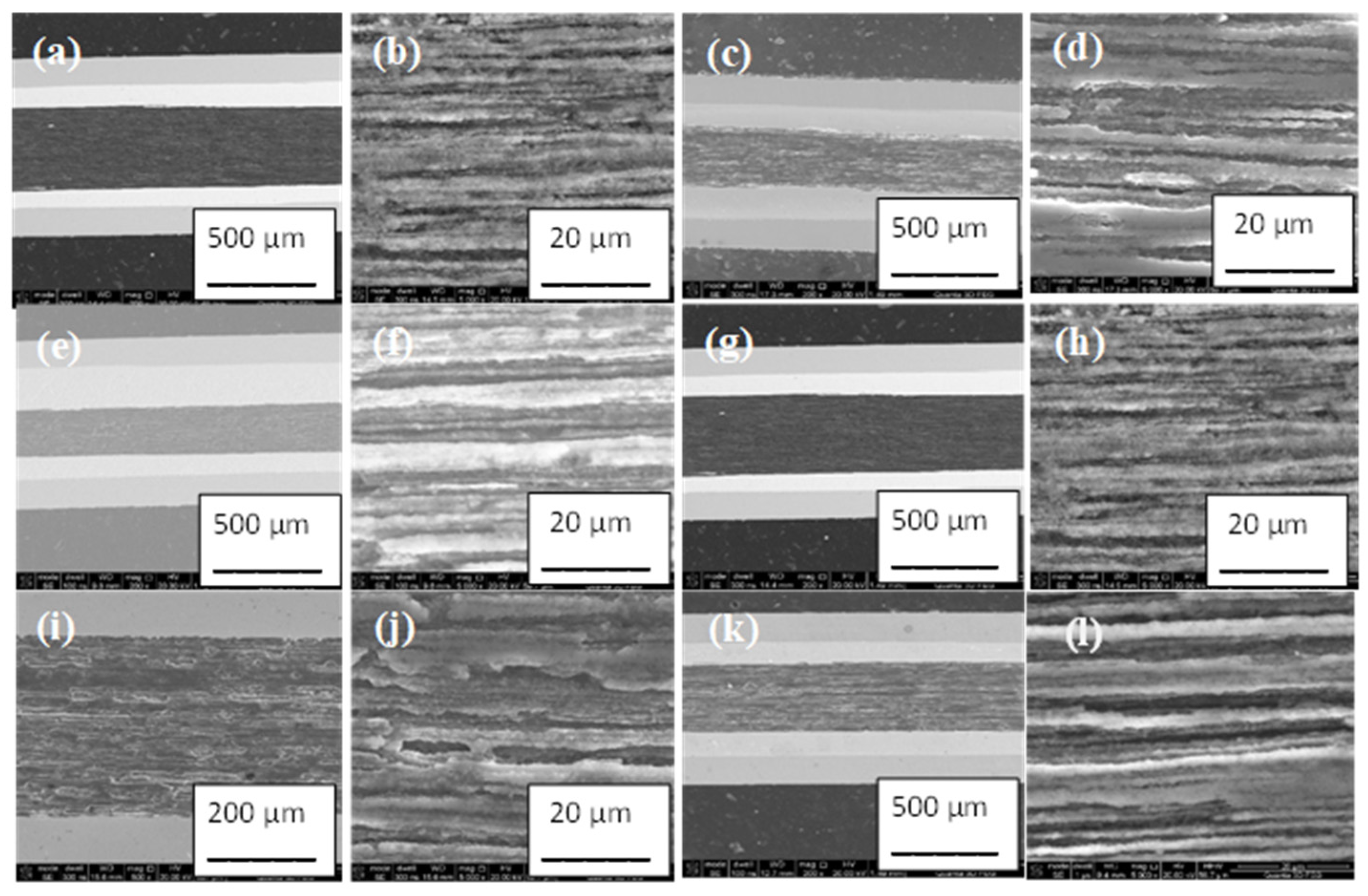
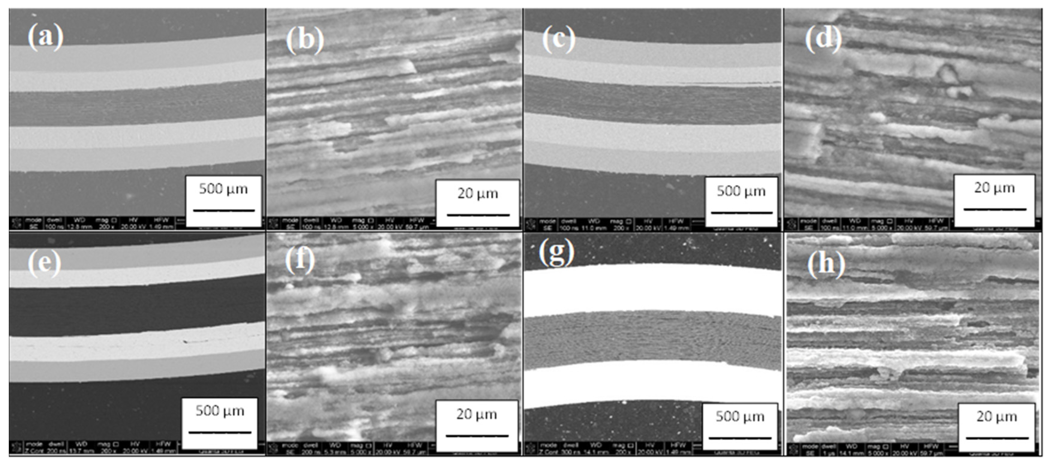
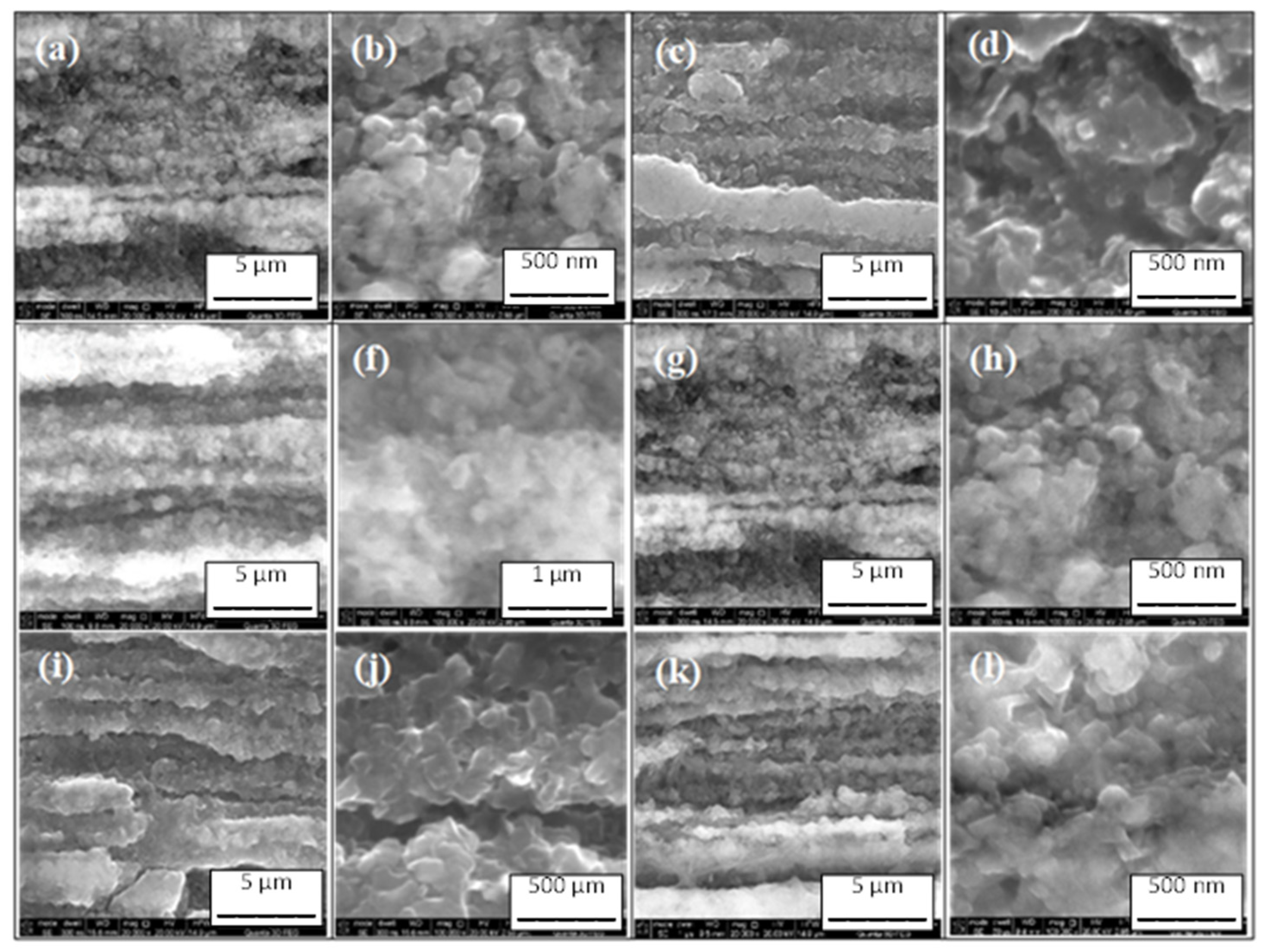
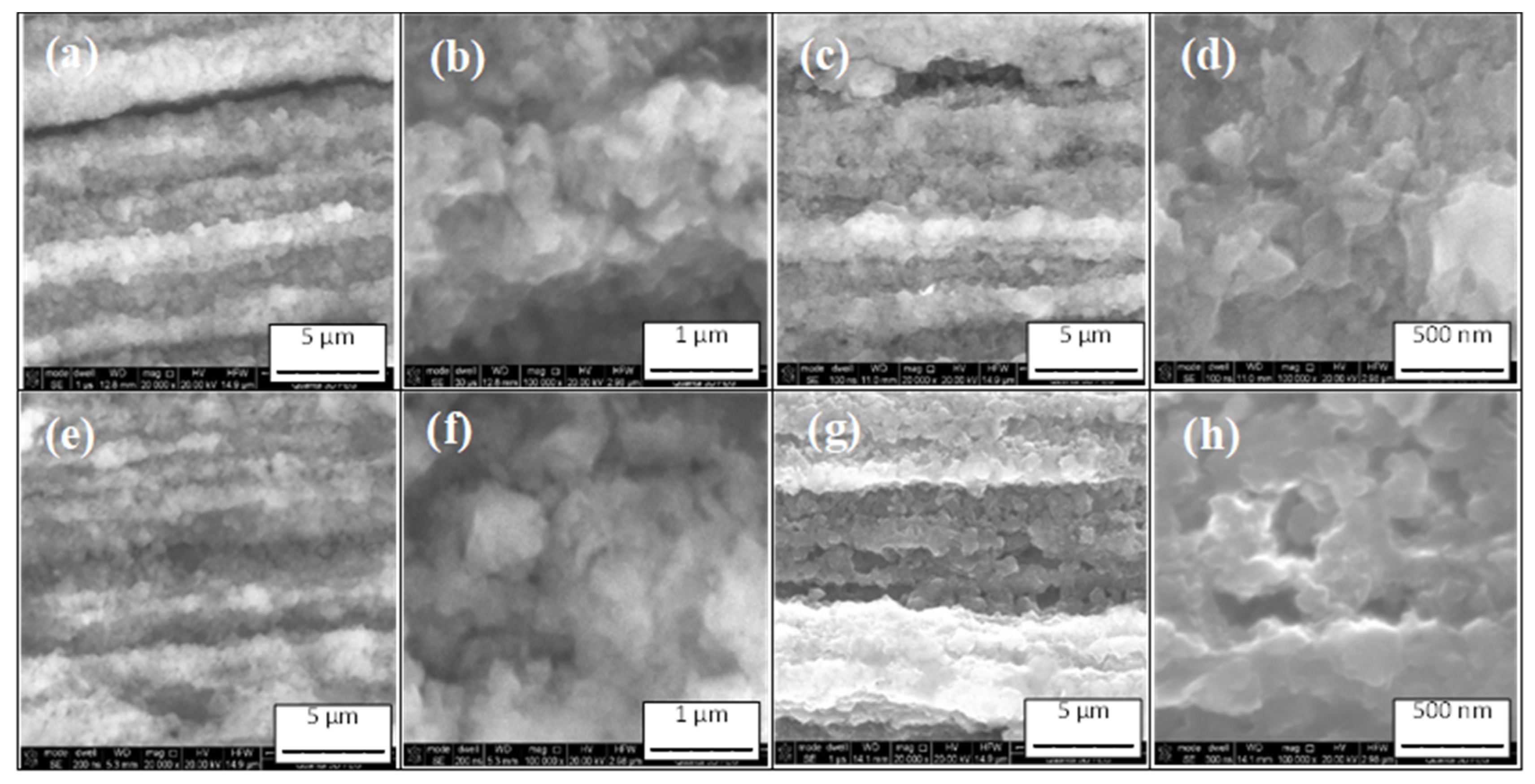
3.1. Structural Analysis of Straight 2% C-Doped MgB2 Wires and Small 2% C-Doped MgB2 Coils

The tightness of the Nb barrier in the 2% C-doped MgB2 wires was checked using the field sweep [27] and temperature sweep [28] methods and with a scanning electron microscope. Both methods showed that there were no cracks in the Nb barrier. Studies have shown that cracks in the Nb barrier significantly reduce Jc in MgB2 wires [27]. For MgB2 coils made with the wind-and-react method, the tightness of the Nb barrier is very important because it allows one to obtain high Jc and homogeneous structure of the MgB2 material in wires over a length of several kilometers.
The EDS analysis of straight wires and small coils showed that the 2% C-doped MgB2 material had a homogeneous distribution of Mg and B, and it had a very consistent, near-stoichiometric atomic (e.g., B—62.3–65.4%; Mg—34.6–37.7%) and weight (e.g., B—78.8–8.9%; Mg—19.1–21.2%) composition. This is very important because it allows us to obtain uniform critical parameters on long MgB2 wires (above 1 km). This increases the application possibilities of MgB2 wires.
Transverse cracks strongly reduce the critical-current density in MgB2 wires. It is clearly seen (Figure 1) that no transverse cracks appeared in the structure of the 2% C-doped MgB2 material in the longitudinal section of wires. The SEM results in Figure 1 showed that the 2% C-doped MgB2 material had a layered structure. Studies show that annealing at 610 °C, 630 °C, and 650 °C for 2 h and 6 h allowed similar morphologies of the 2% C-doped MgB2 material to be obtained in all samples. Further results show that a longer annealing time (12 h) at 630 °C and 650 °C improved the layered structure (Figure 1i–l). On the other hand, the long annealing time (12 h) at 610 °C did not improve the layered structure, which was similar to the structure of samples annealed for 2 h and 6 h at 610 °C, 630 °C, and 650 °C. This indicates that the synthesis reaction in the 2% C-doped MgB2 material at 610 °C is very slow. Our results also indicate that the reaction in the liquid state of Mg at 650 °C is not significantly faster than the synthesis reaction in the solid state of Mg at 630 °C, even over a very long time (12 h).
The results in Figure 2 show the longitudinal sections of 2% C-doped MgB2 wires on small-diameter coils of 10 mm and 20 mm. These SEM images show that the small-diameter bending of the MgB2 wire did not create any cracks in the structure of the 2% C-doped MgB2 material (Figure 2). This is very important for applications in superconducting coils. Further results show that bending did not affect the layered structure. The layered structure is very important because it creates a large number of longitudinal connections that allow a high Jc value to be obtained. In addition, this research shows that bending did not affect the synthesis reactions in solid-state and liquid-state Mg, because the structure of the 2% C-doped MgB2 material on the coils was similar to the structure of the 2% C-doped MgB2 material on straight wires (Figure 2).
In Figure 3 (high magnification), we see that after annealing at temperatures of 610 °C, 630 °C, and 650 °C for 2 h and 6 h, the samples did not have cracks and had similar grain sizes. Additionally, the results in Figure 3 show that the sample annealed at 630 °C for 2 h had slightly better grain connections. The next results show that a long annealing time (12 h) and annealing temperatures of 630 °C and 650 °C significantly improved the connections among the grains (Figure 3). On the other hand, annealing at 610 °C for 12 h did not improve the connections among grains (Figure 3).
Figure 4 shows that unreacted 2% C-doped MgB2 wire bending with small diameter and thermal treatment did not create micro- and nanocracks among grains and did not affect the size and growth rate of grains. Our research shows that the morphology of the 2% C-doped MgB2 material on straight and bent wires was similar (Figure 3 and Figure 4).

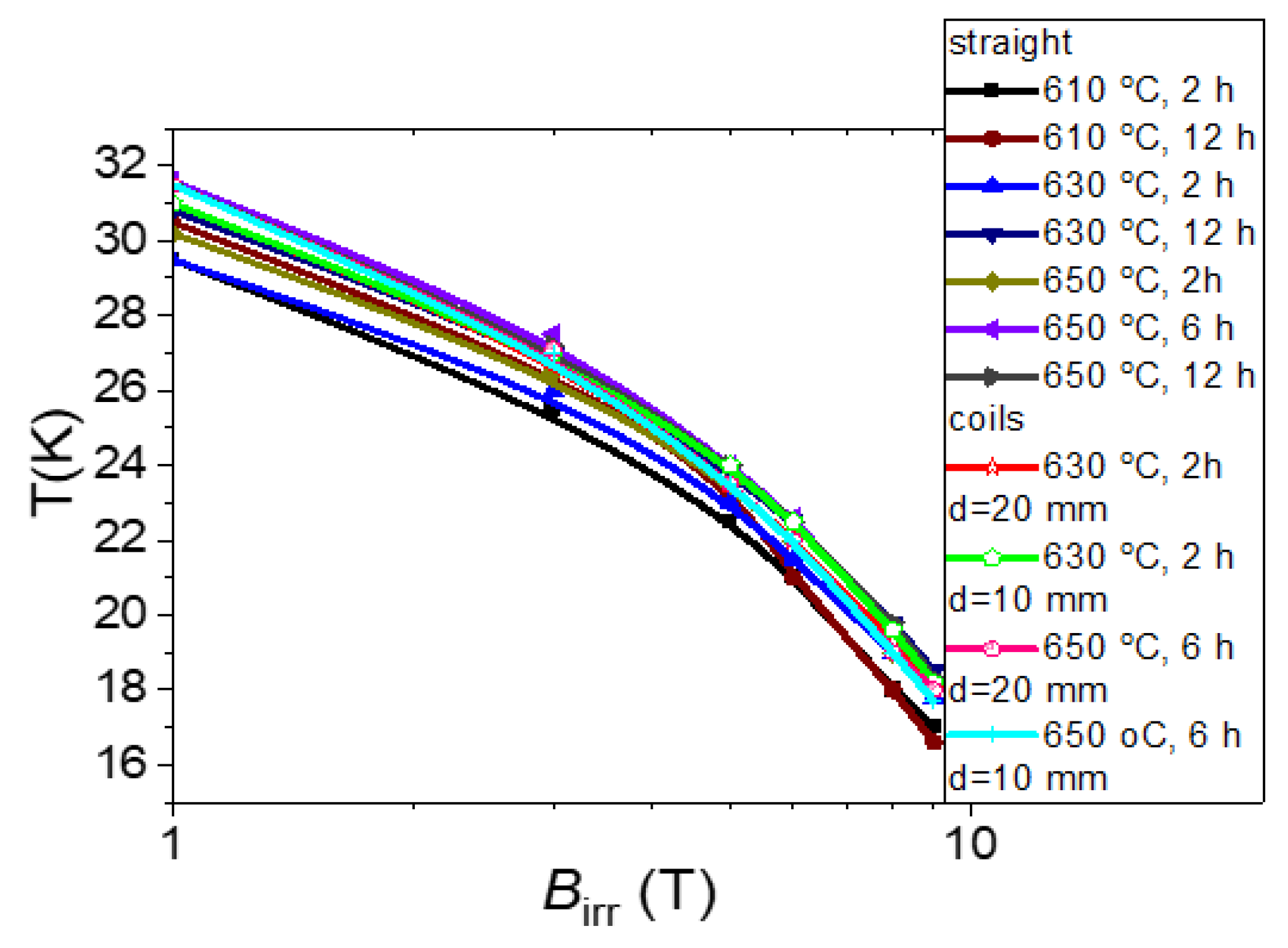
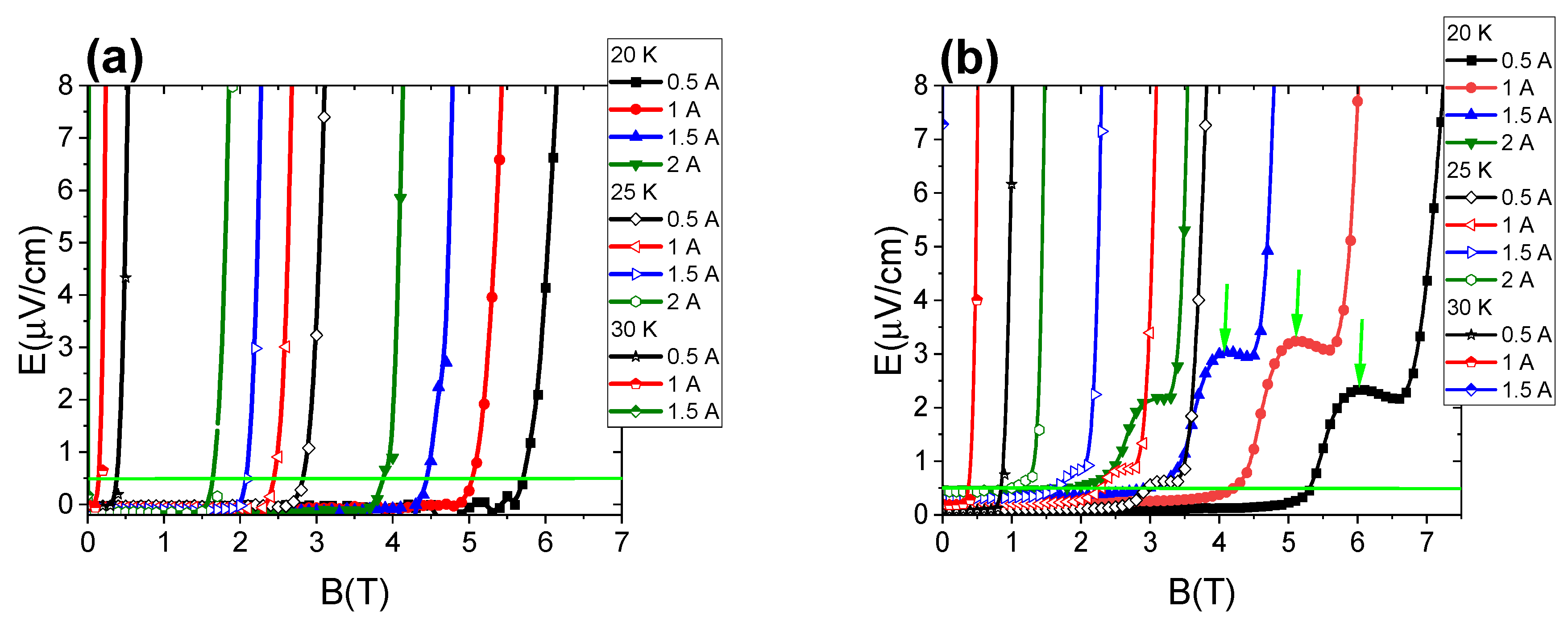
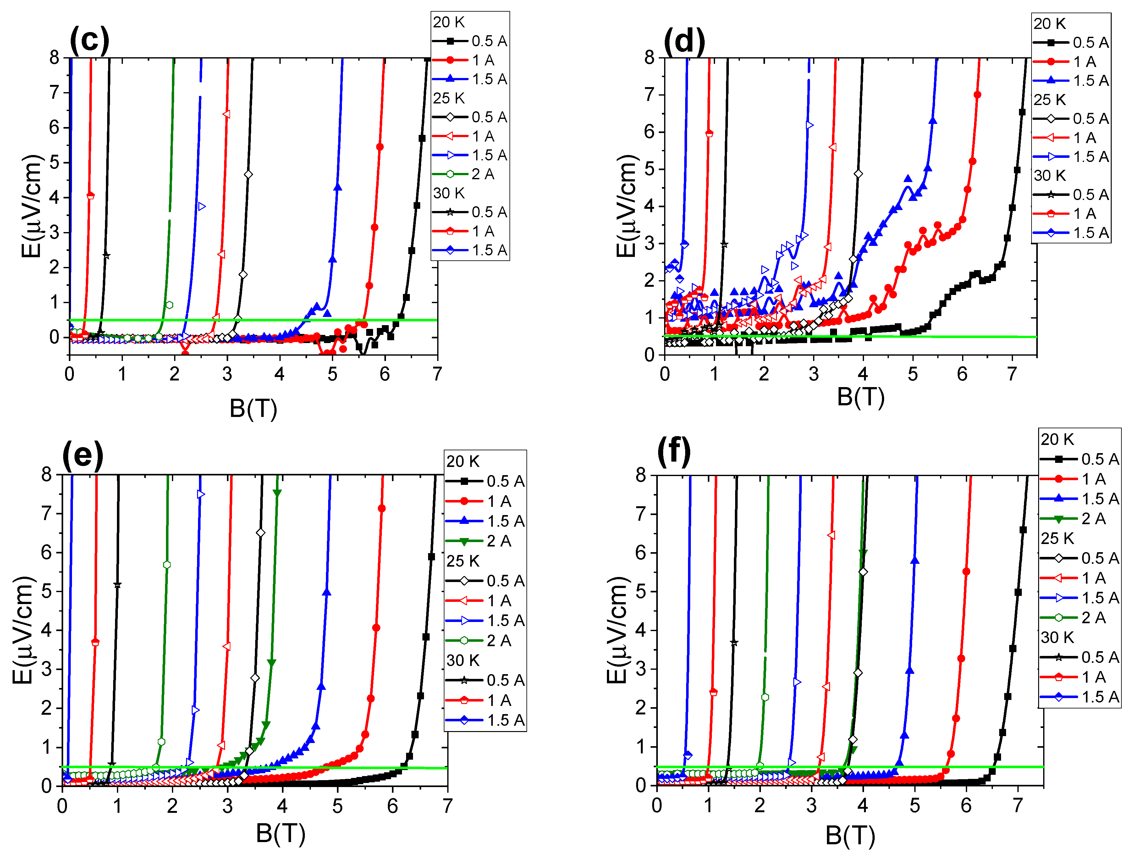
3.2. Irreversible-Magnetic-Field Analysis of Straight 2% C-Doped MgB2 Wires and Small 2% C-Doped MgB2 Coils

The results of the transport measurements showed that increasing the annealing time from 2 h to 12 h at 610 °C slightly increased Tc (from 32.2 to 32.5 K). Further results show that increasing the annealing time from 2 h to 12 h at 630 °C led to an increase in Tc from 32.5 to 33.5 K. The next results show that increasing the annealing time from 2 h to 6 h at 650 °C increased Tc from 33.5 to 35 K. A further increase in the annealing time (12 h) did not increase Tc. The measurements indicate that increasing the annealing temperature from 610 °C to 650 °C for 2 h increased Tc by 1.3 K. On the other hand, increasing the annealing temperature from 610 °C to 650 °C for 12 h led to an increase in Tc by 2.5 K. Earlier studies showed that the critical temperature (Tc) is dependent on stress, strain, stoichiometry, doping, pressure, coherence length, free path, and the lattice parameter [22,29]. These results indicate that a higher annealing temperature and a longer annealing time allowed us to obtain 2% C-doped MgB2 material with higher Tc, because we obtained a material more similar to the MgB2 superconducting phase with a critical temperature of 39 K. The increase in Tc indicates that the process of substituting carbon for boron is not significant while heating at low temperature.
Previous research indicates that the irreversible magnetic field in superconducting materials depends on the pinning centers [24,30]. The results in Figure 5 show that increasing the annealing time from 2 h to 12 h at 610 °C led to an increase in Birr in the high-temperature range (26 K to 30 K) and did not increase Birr below 26 K.
The results in Figure 6a,b indicate the cause of the change in Birr of sample G. The transport results in Figure 6b show the peak effect of resistance (red arrow) in the temperature range of 16 K to 24 K. This is the first time this effect has been observed in 2% C-doped MgB2 wires depending on the temperature. Previously, a similar effect was observed in NbTi wires depending on the magnetic field [24] and in MgB2 crystals depending on the magnetic field [31]. In NbTi wires, this effect was related to the strong trapping of the vortex lattice by different pinning centers in different ranges of magnetic fields [24]. In MgB2 crystals, this effect was the result of the pinning forces for the motion of vortex spots transverse to the applied field becoming larger than those for parallel motion, and the anisotropic vortex current distribution induced a reduced energy barrier for vortex nucleation at the edge perpendicular to the field [31]. The above results indicate that the resistance peak obtained is related to the low density of pinning centers close to Birr. The results in Figure 6b show, for the first time, the effect of individual pinning centers on Birr depending on the temperature. Based on these results, we can indicate that high-field and high-temperature pinning centers (pinning centers trap vortex lattices from 25 K to 30 K) poorly trap the vortex lattice at middle temperatures and in high magnetic fields. In addition, the results indicate that high-field and middle-temperature (from 16 K to 25 K) pinning centers poorly trap the vortex lattice in high magnetic fields and at high temperatures. This is a very important measurement result, because it allows us to better understand the effect of the trapping process of the vortex lattice on structural defects. These results also show that at low annealing temperatures, high-field and low-temperature pinning centers form much more slowly than low-field and high-temperature pinning centers. Further results in Figure 6c,d show that higher annealing temperature and longer annealing time increase the number of high-field and middle-temperature pinning centers and remove the resistance peak. This suggests that high-field pinning centers may form a carbon-for-boron substitution. This process at low annealing temperatures is slow and produces a small number of pinning centers. That is why we see a resistance peak.
Further results show that increasing the annealing temperature from 610 °C to 630 °C for 2 h led to an increase in Birr at moderate temperatures and high magnetic fields (Figure 5). This indicates that it creates more high-field and low-temperature pinning centers. An increase in the annealing time from 2 h to 12 h at an annealing temperature of 630 °C led to an increase in Birr at low, middle, and high temperatures. This indicates that this annealing process can create low-, mid-, and high-field pinning centers. A further increase in the annealing temperature from 630 °C to 650 °C for 2 h led to an increase in Birr at high temperatures. This indicates that it mainly forms high-temperature pinning centers. The increase in the annealing time from 2 h to 12 h at 650 °C led to a slight increase in Birr.
The next results show that small coils, after annealing at 630 °C for 2 h, had a Birr value that was 10% higher than that of a straight 2% C-doped MgB2 wire from the same annealing process. Previous results showed that small coils and simple coils had the same Birr [12]. However, these processes were performed in liquid Mg. Our heating process for J and K coils involved solid-state Mg. This may indicate that cold bending and heat treatment in the solid state of Mg can yield more pinning centers. Further results show that small coils and straight wires annealed at 650 °C for 6 h had similar Birr. This indicates that cold bending and thermal treatment in the liquid state of Mg do not affect the formation of pinning centers.
The transport measurements in Figure 6 show that our samples did not exhibit magnetoresistance. This indicates that no unreacted Mg remained in our samples after the heat treatment process. Our MgB2 wire was made with a Nb barrier, a Monel sheath, and a 2% C-doped MgB2 core. All these components have higher resistance than pure Mg. The next results show that increasing the annealing temperature from 630 °C to 650 °C led to a decrease in resistance in the normal state by approximately 15%, especially for the 2 h annealing time. This indicates that a higher annealing temperature allows for a greater number of connections among grains. Further results show that a longer heating time (2 h to 12 h) at 610 °C reduced resistance in the normal state by 22%. On the other hand, increasing the heating time (2 h to 12 h) at 630 °C reduced resistance in the normal state by approximately 15%. The next transport measurements showed that an increase in the annealing time (2 h to 6 h) for the annealing temperature of 650 °C led to a decrease in resistivity in the normal state by 30%. A longer heating time at 650 °C did not reduce resistance in the normal state. This indicates that a longer annealing time allows a greater number of connections to be obtained among grains. Moreover, the results in Figure 6 indicate that the samples had a narrow superconducting-state-to-resistive-state transition. We observed such effects for all heating times and temperatures and for small coils. This shows that the MgB2 wires have high homogeneity of 2% C-doped MgB2 material. These factors are important for the design of superconducting coils.

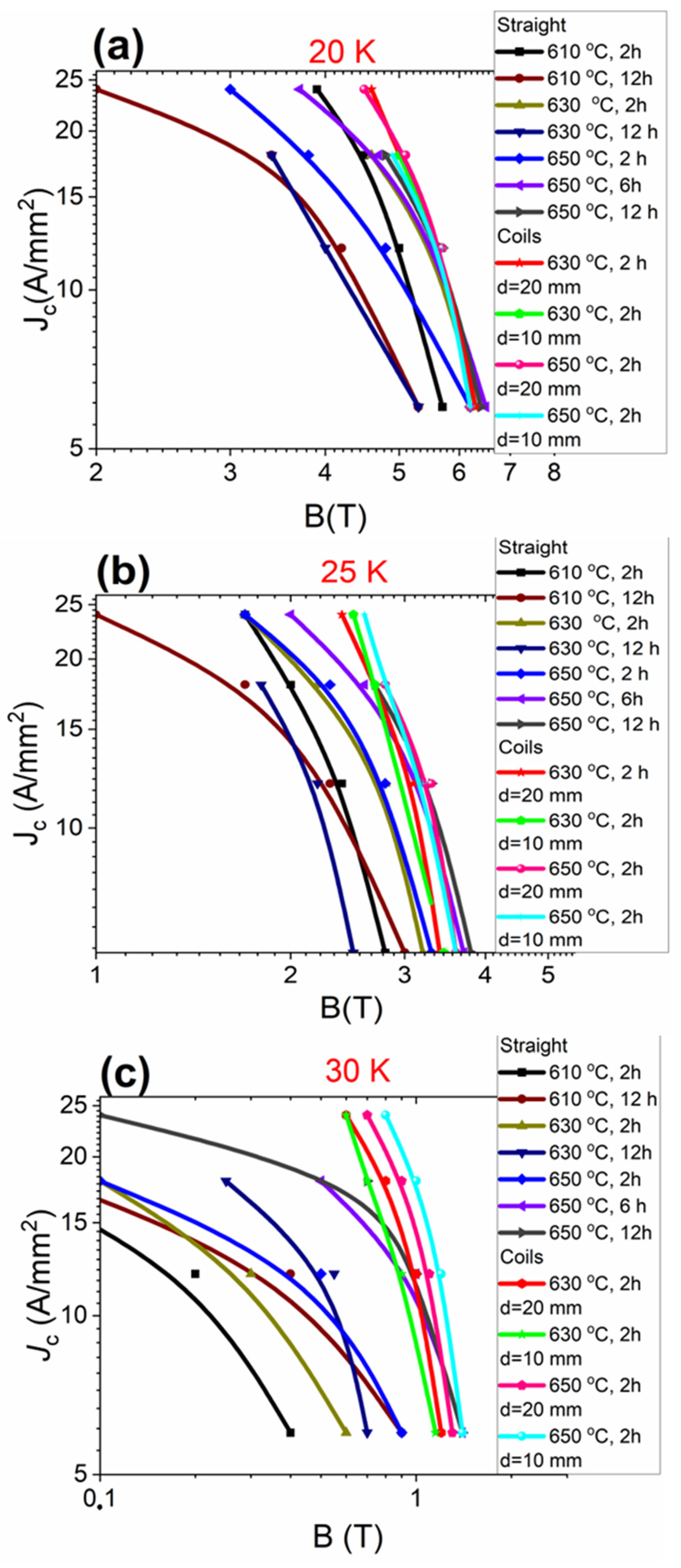
3.3. Critical-Current Density in Straight 2% C-Doped MgB2 Wires and Small 2% C-Doped MgB2 Coils

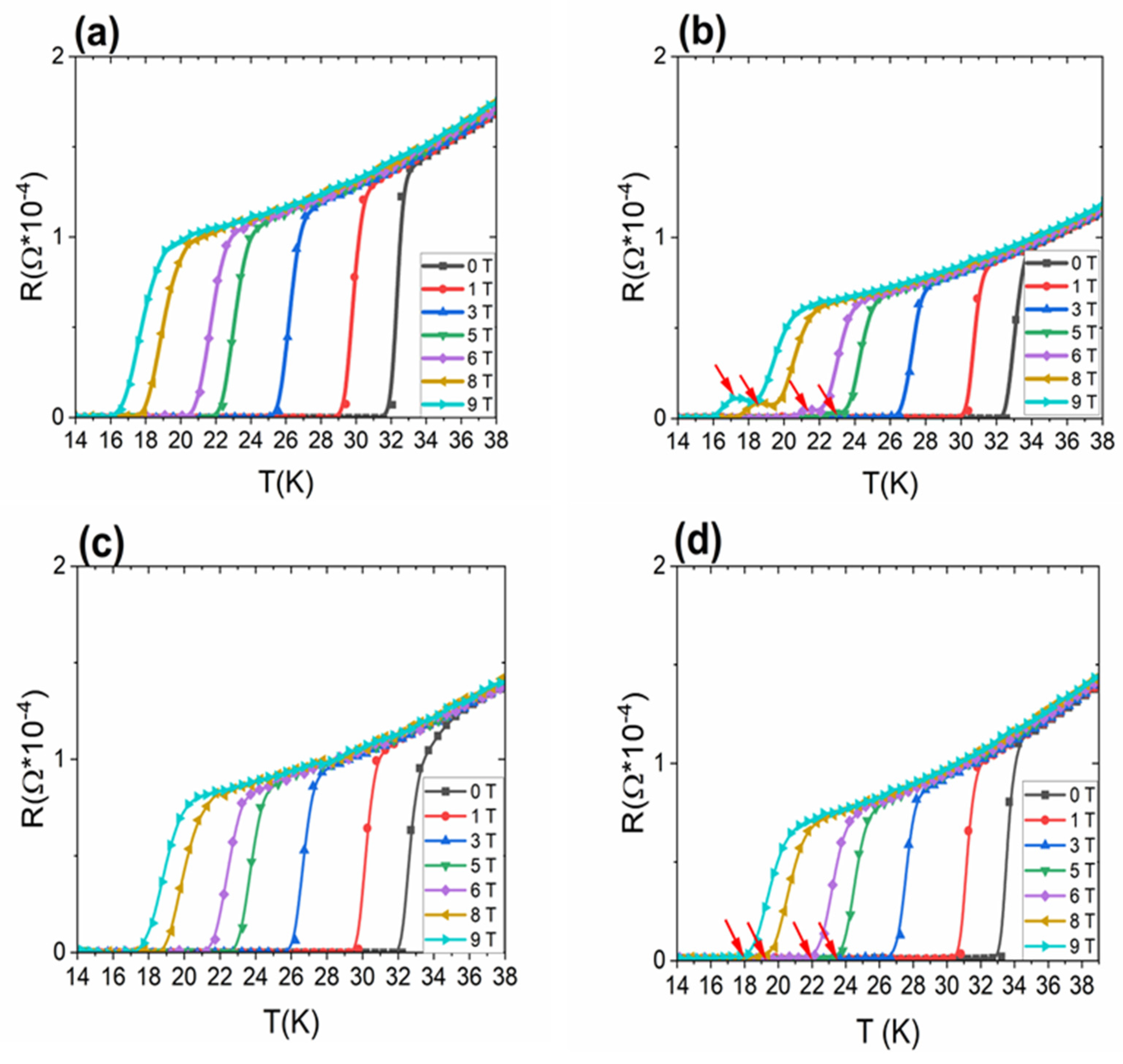
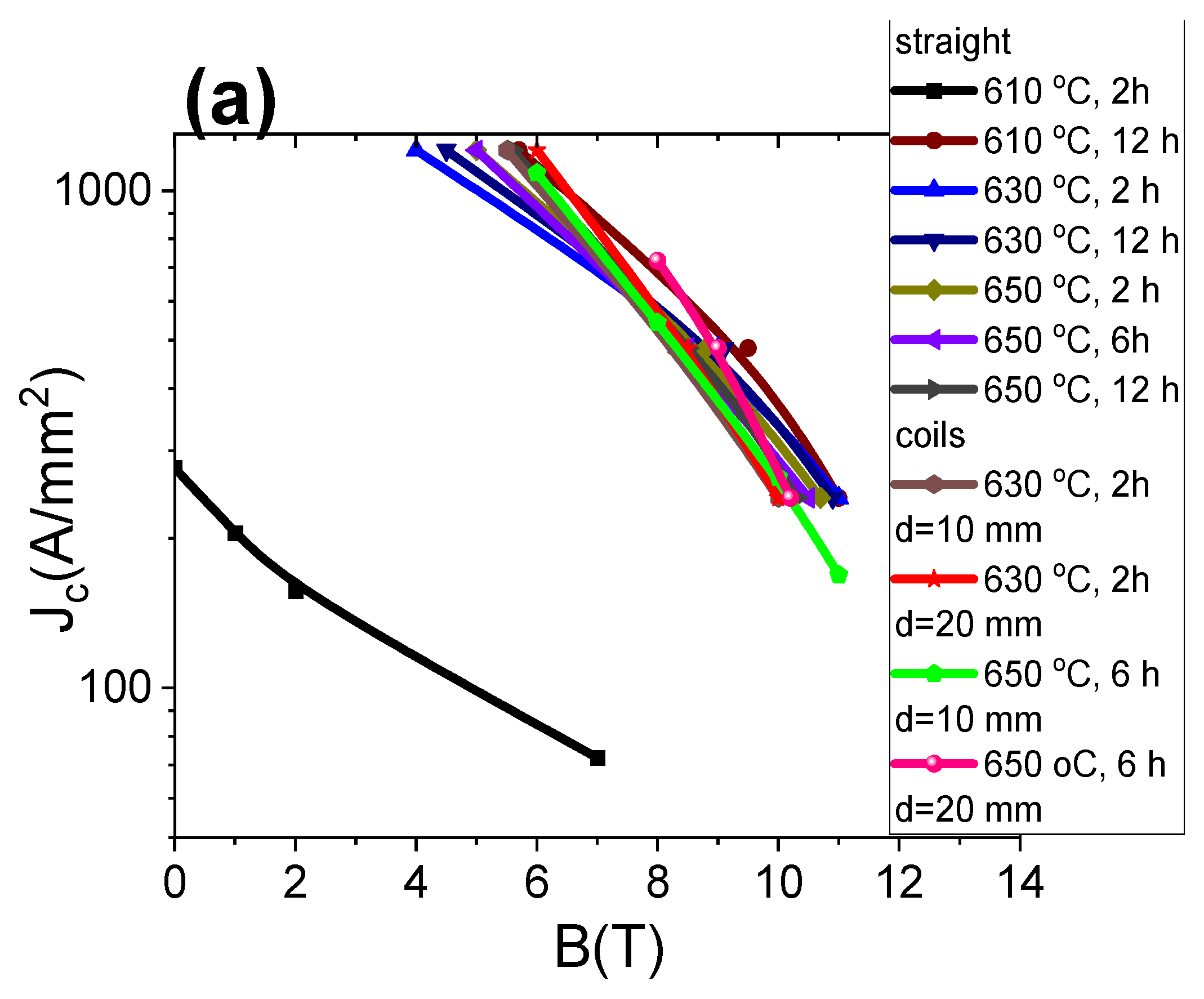
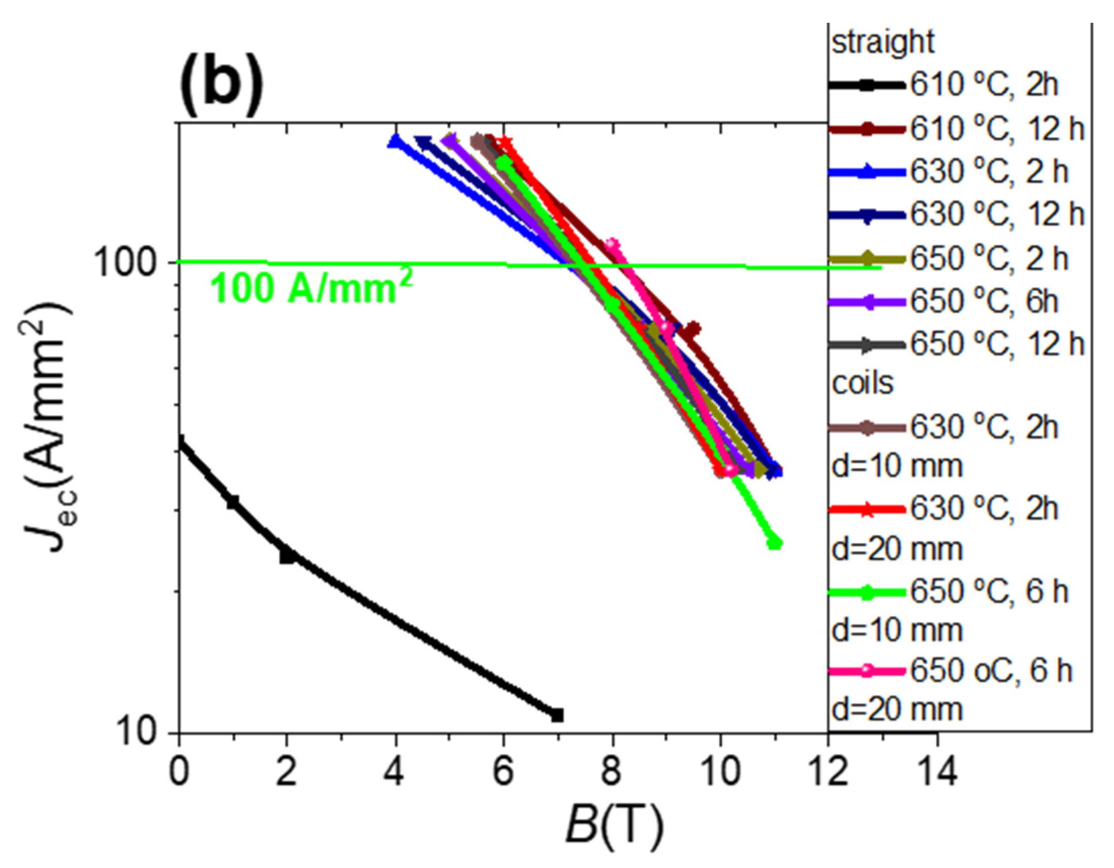
3.3.1. Jc and Jec at 4.2 K

The results in Figure 7a show that increasing the annealing time from 2 h to 12 h at 610 °C significantly increased the critical-current density. Further results show that an increase in the annealing temperature and annealing time did not lead to an increase in Jc at 4.2 K. Additionally, the results show that Jc at 4.2 K for small coils was the same as Jc for straight MgB2 wires. This indicates that the wind-and-react (W&R) method is very good, because it does not lead to the degradation of Jc even on large bends (diameter of 10 mm). Our results also indicate that low annealing temperatures can be used for annealing the coils. This is important because it reduces the costs of coil production. In addition, we obtained a very high Jc value of 400 A/mm2 (4.2 K in 10 T) in powder-in-tube (PIT) 2% C-doped MgB2 wires. The Jc value in our PIT 2% C-doped MgB2 wires is very similar to the Jc in wires and small coils made using internal Mg diffusion (450 A/mm2, 4.2 K, 10 T, 650 °C for 5 h) [32]. Our results indicate that a low annealing temperature has great potential for increasing Jc in wires and coils.
The results in Figure 7b show the engineering critical-current density (Jec) values for straight wires and small coils. Jec was determined for the whole wire (superconducting material, Nb barrier, Monel sheath). Jec is a very important factor in the design of superconducting coils. Currently, the application criterion for superconducting coils is a Jec value of 100 A/mm2. Our results in Figure 7b show that a low annealing temperature allows one to obtain straight wires and small coils with a Jec value of 100 A/mm2 at 8.2 T. This indicates that our wire can be used to produce coils with a magnetic field of 8 T.

3.3.2. Jc at 20 K, 25 K, and 30 K

The critical-current (Ic) measurements at 20 K, 25 K, and 30 K were performed using a PPMS. The critical current was determined based on the criterion of 0.5 µV/cm, because the voltage contacts were 5 mm apart.
By analyzing the measurements in Figure 8a,b, we see that a longer annealing time (from 2 h to 12 h) at 610 °C led to the formation of the electric-field peak (green arrows). This peak is the greatest at 20 K and disappears with a temperature increase from 20 to 30 K.
A similar resistance peak was observed in MgB2 crystals by Rydh et al. [31], but this peak increased with the increase in temperature (from 23 K to 27 K).
This electric-field peak is the result of the low density of the high-field pinning centers. A similar effect was observed in NbTi wires. This effect is called peak effect. This means that we obtain a higher Jc value close to Birr or Bc2 [24] than middle and low magnetic fields. The decrease in the electric-field value may be because high-field pinning centers poorly trap the vortex lattice at middle temperatures (20 K and 25 K). Therefore, there is a smaller peak of the electric field at 25 K than at 20 K, and it decays at 30 K. This shows the properties of high-field pinning centers. In addition, the results show that a longer annealing time at 610 °C decreased Ic, especially at 20 K and 25 K, and increased Ic at 30 K. This indicates that a longer annealing time is necessary to produce high-field and high-temperature pinning centers. Moreover, the results indicate that long annealing times created more pinning centers at 30 K. Figure 8a,b show that high-field pinning centers effectively increased Ic at 20 K and 25 K.
The results of transport measurements in Figure 8c,d show that increasing the annealing time from 2 h to 12 h at 630 °C led to a decrease in Ic in high magnetic fields at 20 K and 25 K and to an increase in Ic at 30 K. This indicates that a long annealing time removes high-field pinning centers, e.g., dislocations, stresses, and strains. These results also indicate that high-field pinning centers can increase Ic at 20 K and 25 K and do not increase Ic at 30 K. In addition, this also indicates that high-temperature pinning centers do not increase Ic at 20 K and 25 K. The electric field in Figure 8d in the zero magnetic field is the result of current penetration into the superconducting material. The overlapping of the curves for the same current (e.g., 0.5 A) at different temperatures and for the increase in the magnetic field is also the effect of current penetration into the superconducting material. This effect disappears for long MgB2 wires.
Further results show that an increase in the annealing temperature from 630 °C to 650 °C for 2 h led to a strong decrease in Ic at 20 K, a weak decrease in Ic at 25 K, and an increase in Ic at 30 K. In addition, in Figure 8e, an electric field appears before exceeding the criterion of 0.5 µV/cm, especially at 20 K and 25 K. This effect disappears at 30 K. The appearance of the electric field before exceeding the 0.5 µV/cm criterion is very unfavorable, because it significantly reduces the critical current that can be used by superconducting coils. Superconducting coils are made of several kilometers of MgB2 wire. Even a small electric field over a distance of 5 mm (distance of voltage contacts) leads to a large electric field on wires several kilometers long. This leads to the heating of the coil and its transition to the resistive state. In addition, based on the results in Figure 8c,e, it was seen that during the annealing process at 650 °C for 2 h, high-field pinning centers at 20 K and 25 K formed more slowly than during the annealing process at 630 °C for 2 h. This indicates that higher density of high-field pinning centers is formed during the reaction in the solid state of Mg than in the liquid state of Mg. These results also indicate that we obtained higher density of high-temperature pinning centers (30 K) during the reaction in the liquid state of Mg than in the solid state of Mg. Further results show that increasing the annealing time from 2 h to 6 h at 650 °C (Figure 8e,f) led to an increase in Ic at 20 K, 25 K, and 30 K and eliminated the effect of increasing the electric field before exceeding the criterion of 0.5 µV/cm. These results indicate that a longer annealing time at 650 °C and Mg in the liquid state allow for an increase in the density of high-field pinning centers and high-temperature pinning centers. It is very important that the electric field decays before exceeding the criterion of 0.5 µV/cm, because it allows for the use of higher Ic values in superconducting coils.
Based on the results in Figure 9a,b, increasing the annealing time from 2 h to 12 h at 610 °C and 630 °C led to a significant decrease in Jc at 20 K and 25 K. On the other hand, increasing the annealing time from 2 h to 12 h at 650 °C led to a significant increase in Jc at 20 K and 25 K. Increasing the annealing temperature from 610 °C to 630 °C for 2 h led to an increase in Jc in high magnetic fields at 20 K and 25 K. A further increase in the annealing temperature to 650 °C caused a significant decrease in Jc at 20 K and did not influence Jc at 25 K. These results indicate that the long annealing time (12 h) at 610 °C and 630 °C and the short annealing time (2 h) at 650 °C did not allow us to obtain high density of high-field pinning centers at 20 K and 25 K. Our results also indicate that high-field pinning centers at 20 K formed much more slowly at an annealing temperature of 650 °C than at 630 °C (2 h). The results show that the Jc values at 20 K and 25 K of small coils and straight wires were similar. This is very important because it shows that the wind-and-react (W&R) method does not reduce Jc in the coil.
The results in Figure 9c show that increasing the annealing time from 2 h to 12 h at 610 °C, 630 °C, and 650 °C led to an increase in Jc at 30 K. Further results show that increasing the annealing temperature from 610 °C to 650 °C for 2 h and 12 h also led to an increase in Jc at 30 K. These results show that we can obtain a higher density of high-temperature pinning centers as a result of the longer heating time and increase in the annealing temperature. The results show that small coils after annealing at 630 °C for 2 h had a much higher Jc value at 30 K than straight wires after annealing at the same temperature. Further results indicate that coils, after annealing at 650 °C for 6 h, also had higher Jc at 30 K than straight wires after annealing at the same temperature. This result indicates that more high-temperature pinning centers formed on the coils. This effect was not visible at 20 K and 30 K. This is a very interesting and important result for future applications. This effect may be related to the change in the density of the unreacted MgB2 material in the wire after bending. Our research has shown that higher density of unreacted MgB2 material improves critical parameters at low annealing temperatures [33].

4. Conclusions

Our research showed that low–temperature annealing in the temperature range of 610 °C to 650 °C allowed us to obtain a structure with a similar morphology, e.g., thickness of layers, grain size and voids, and connections among grains. Studies have shown that a longer annealing time (12 h) at temperatures of 630 °C and 650 °C improves the connections between layers. Further studies showed that the structures of the 2% C-doped MgB2 material on straight wires and bent wires, even with small diameters, are similar. In addition, the tests showed that bending and heat treatment at low annealing temperatures did not cause transverse cracks in the 2% C-doped MgB2 material or the Nb barrier and Monel shield. This indicates that the wind-and-react method can be used to manufacture 2% C-doped MgB2 superconducting coils. Measurements showed that a longer annealing time and a higher annealing temperature allowed for an increase in the critical temperature (Tc). The highest Tc measured at 35 K was obtained with the annealing process at 650 °C for 6 h. The performed studies showed that a longer annealing time was necessary to obtain high Birr at an annealing temperature of 610 °C. On the other hand, the measurements showed that a longer annealing time at 630 °C led to a decrease in Birr. The next measurement results indicate that a longer annealing time was necessary to increase Birr at 650 °C. The results show that the Birr of straight wires was close to the Birr of coils. This is very important because it indicates that bending does not cause Birr degradation during annealing when magnesium is in a solid or liquid state.
Further results show that increasing the annealing time at 610 °C led to a significant increase in Jc at 4.2 K. Moreover, higher annealing temperatures and longer annealing times did not lead to a significant increase in Jc at 4.2 K. Our results show that low-temperature annealing can produce very high Jc at 4.2 K–400 A/mm2 at 10 T. Calculations show that our wires had very high engineering critical-current density, 100 A/mm2 at 8 T. This allowed us to produce coils with a magnetic field of 8 T.
Our results show that a low annealing temperature of 610 °C and 630 °C for 2 h allowed us to obtain high Jc at 20 K. Further studies showed that the annealing temperatures of 610 °C and 630 °C led to a significant reduction in Jc at 30 K. Further studies showed that the annealing temperature of 650 °C allowed us to obtain the highest Jc at 30 K. Transport measurements also showed that coils annealed at 630 °C had a Jc value similar to that of straight wires at 20 K and 25 K and much higher Jc at 30 K. Further results show that coils annealed at 650 °C for 6 h had a Jc value similar to that of straight wires at 20 K, 25 K, and 30 K.
Our results show that middle-temperature and high-field pinning centers increased Jc in the temperature range of 16 K to 25 K and did not influence Jc in the temperature range of 25 K to 30 K. Further measurement results show that high-temperature and high-field pinning centers increased Jc in the temperature range from 25 K to 30 K and had a weak effect on Jc in the temperature range from 16 K to 25 K. These measurement data are very important because they could allow us to better optimize the production process of superconducting coils depending on the temperature (e.g., 20 K, 30 K) at which the coil generates a magnetic field.

Author Contributions

Conceptualization, D.G. and T.C.; methodology, M.B.; validation, D.G., T.C., and M.R.; formal analysis, A.Z.; investigation, D.G. and M.B.; resources, T.C.; data curation, D.G.; writing—original draft preparation, D.G.; writing—review and editing, T.C. and M.R.; visualization, D.G.; supervision, A.Z.; project administration, T.C.; funding acquisition, T.C. All authors have read and agreed to the published version of the manuscript.

Funding

This research was funded by the statutory sources of the Department of Materials Technology, Military University of Technology (project No. UGB 808/2023/WAT).

Institutional Review Board Statement

Not applicable.

Informed Consent Statement

Not applicable.

Data Availability Statement

Not applicable.

Conflicts of Interest

The authors declare no conflict of interest.

References

  1. Zhang, Y.; Liu, W.; Zhu, X.; Zhao, H.; Hu, Z.; He, C.; Wen, H.H. Unprecedented high irreversibility line in the nontoxic cuprate superconductor (Cu,C)Ba2Ca3Cu4O11+δ. Sci. Adv. 2018, 4, 0192. [Google Scholar] [CrossRef]
  2. Galluzzi, A.; Buchkov, K.; Tomov, V.; Nazarova, E.; Leo, A.; Grimaldi, G.; Polichetti, M. High pinning force values of a Fe (Se, Te) Single crystal presenting a second magnetization peak phenomenon. Materials 2021, 14, 5214. [Google Scholar] [CrossRef]
  3. Moon, I.Y.; Kim, S.J.; Lee, H.W.; Jung, J.; Oh, Y.S.; Kang, S.H. Investigation of the correlation between initial microstructure and critical current density of Nb-46.5 wt%Ti superconducting material. Metals 2021, 11, 777. [Google Scholar] [CrossRef]
  4. Bovone, G.; Buta, F.; Lonardo, F.; Bagni, T.; Bonura, M.; LeBoeuf, D.; Hopkins, S.C.; Boutboul, T.; Ballarino, A.; Senatore, C. Effects of the oxygen source configuration on the superconducting properties of internally-oxidized internal-Sn Nb3Sn wires. Supercond. Sci. Technol. 2023, 36, 095018. [Google Scholar] [CrossRef]
  5. Yagaia, T.; Mizunoa, S.; Okuboa, T.; Mizuochia, S.; Kamibayashia, M.; Jimboa, M.; Takaoa, T.; Hiranob, N.; Makidac, Y.; Shintomic, T.; et al. Development of design for large scale conductors and coils using MgB2 for superconducting magnetic energy storage device. Cryogenics 2018, 96, 75–82. [Google Scholar] [CrossRef]
  6. Buzea, C.; Yamashita, T. Review of superconducting properties of MgB2. Supercond. Sci. Technol. 2001, 14, R115–R146. [Google Scholar] [CrossRef]
  7. Sumption, M.D.; Bhatia, M.; Rindfleisch, M.; Tomsic, M.; Collings, E.W. Transport and magnetic Jc of MgB2 strands and small helical coils. Appl. Phys. Lett. 2005, 86, 102501–102516. [Google Scholar] [CrossRef]
  8. Tanaka, K.; Kitaguchi, H.; Kumakura, H.; Yamada, H.; Hirakawa, M.; Okada, M. Fabrication and transport properties of an MgB2 solenoid coil. Supercond. Sci. Technol. 2005, 18, 678–681. [Google Scholar] [CrossRef]
  9. Serquis, A.; Civale, L.; Coulter, J.Y.; Hammon, D.L.; Liao, X.Z.; Zhu, Y.T.; Peterson, D.E.; Mueller, F.M.; Nesterenko, V.F.; Indrakanti, S.S. Large field generation with a hot isostatically pressed powder-in-tube MgB2 coil at 25 K. Supercond. Sci. Technol. 2004, 17, L35–L37. [Google Scholar] [CrossRef]
  10. Iwasa, Y. Towards liquid-helium-free, persistent-mode MgB2 MRI magnets: FBML experience. Supercond. Sci. Technol. 2017, 30, 053001. [Google Scholar] [CrossRef] [PubMed]
  11. Soltanian, S.; Horvat, J.; Wang, X.L.; Tomsic, M.; Dou, S.X. Transport critical current of solenoidal MgB2/Cu coils fabricated using a wind-reaction in situ technique. Supercond. Sci. Technol. 2003, 16, L4–L6. [Google Scholar] [CrossRef]
  12. Gajda, D.; Zaleski, A.J.; Morawski, A.; Cetner, T.; Rindfleisch, M. The influence of wire bending and wire diameter on transport critical current density in small MgB2 superconducting coils for applications in multi-section coils. J. Supercond. Nov. Magn. 2020, 33, 3395–3399. [Google Scholar] [CrossRef]
  13. Tomsic, M.; Rindflesich, M.; Yue, J.; McFadden, K.; Phillip, J.; Sumption, M.D.; Bhatia, M.; Bohnenstiehl, S.; Collings, E.W. Overview of MgB2 Superconductor Applications. Int. J. Appl. Ceram. Technol. 2007, 4, 250–259. [Google Scholar] [CrossRef]
  14. Pelissier, J.L. Determination of the phase diagram of magnesium: A model-potential approach in the sub-megabar range. Phys. Scr. 1986, 34, 838–842. [Google Scholar] [CrossRef]
  15. Gajda, D.; Zaleski, A.; Morawski, A.; Cetner, T.; Thong, C.J.; Rindfleisch, M.A. Point pinning centers in SiC doped MgB2 wires after HIP. Supercond. Sci. Technol. 2016, 29, 085010. [Google Scholar] [CrossRef]
  16. Katsura, Y.; Shimoyama, J.; Yamamoto, A.; Horii, S.; Kishio, K. Effects of rare earth doping on the superconducting properties of MgB2. Physica C 2007, 463–465, 225–228. [Google Scholar] [CrossRef]
  17. Wang, X.L.; Soltanian, S.; James, M.; Qin, M.J.; Horvat, J.; Yao, Q.W.; Liu, H.K.; Dou, S.X. Significant enhancement of critical current density and flux pinning in MgB2 with nano-SiC, Si, and C doping. Physica C 2004, 408–410, 63–69. [Google Scholar] [CrossRef]
  18. Woźniak, M.; Juda, K.L.; Hopkins, S.C.; Gajda, D.; Glowacki, B.A. Optimization of the copper addition to the core of in situ Cu-sheathed MgB2 wires. Supercond. Sci. Technol. 2013, 26, 105008. [Google Scholar] [CrossRef]
  19. Shahabuddin, M.; Madhar, N.A.; Alzayed, N.S.; Asif, M. Uniform dispersion and exfoliation of multi-walled carbon nanotubes in CNT-MgB2 superconductor composites using surfactants. Materials 2019, 12, 3044. [Google Scholar] [CrossRef]
  20. Yeoh, W.K.; Cui, X.Y.; Gault, B.; De Silva, K.S.B.; Xu, X.; Liu, H.W.; Yen, H.-W.; Wong, D.; Bao, P.; Larson, D.J.; et al. On the roles of graphene oxide doping for enhanced supercurrent in MgB2 based superconductors. Nanoscale 2014, 6, 6166. [Google Scholar] [CrossRef]
  21. Xu, H.L.; Feng, Y.; Xu, Z.; Yan, G.; Li, C.S.; Mossang, E.; Sulpice, A. Effects of TiB2 doping on the critical current density of MgB2 wires. Physica C 2006, 443, 5–8. [Google Scholar] [CrossRef]
  22. Kazakov, S.M.; Puzniak, R.; Rogacki, K.; Mironov, A.V.; Zhigadlo, N.D.; Jun, J.; Soltmann, Ch.; Batlogg, G.; Karpinski, J. Carbon substitution in MgB2 single crystals: Structural and superconducting properties. Phys. Rev. B 2005, 71, 024533. [Google Scholar] [CrossRef]
  23. Lim, J.H.; Shim, J.H.; Choi, J.H.; Park, J.H.; Kim, W.; Joo, J.; Kim, C.J. Effects of nano-carbon doping and sintering temperature on microstructure and properties of MgB2. Physica C 2009, 469, 15–20. [Google Scholar] [CrossRef]
  24. Gajda, D.; Zaleski, A.; Morawski, A.; Hossain, M.S.A. New types of high field pinning centers and pinning centers for the peak effect. Supercond. Sci. Technol. 2017, 30, 085011. [Google Scholar] [CrossRef]
  25. Huang, X.; Mickelson, W.; Regan, B.C.; Zettl, A. Enhancement of the upper critical field of MgB2 by carbon-doping. Solid State Commun. 2005, 136, 278–282. [Google Scholar] [CrossRef]
  26. Serquis, A.; Civale, L.; Hammon, D.L.; Liao, X.Z.; Coulter, J.Y.; Zhu, Y.T.; Jaime, M.; Peterson, D.E.; Mueller, F.M.; Nesterenko, V.F.; et al. Hot isostatic pressing of powder in tube MgB2 wires. Appl. Phys. Lett. 2003, 82, 2847. [Google Scholar] [CrossRef]
  27. Gajda, D.; Zaleski, A.J.; Morawski, A.; Rindfleisch, M.; Thong, C.; Tomsic, M. The electric field jump—Detection of damaged Nb barrier in MgB2 wires annealed under pressure. Supercond. Sci. Technol. 2015, 28, 115003. [Google Scholar] [CrossRef]
  28. Gajda, D.; Morawski, A.; Zaleski, A.; Yamamoto, A.; Cetner, T. A defect detection method for MgB2 superconducting and iron-based Ba(Fe,Co)2As2 wires. Appl. Phys. Lett. 2016, 108, 152601. [Google Scholar] [CrossRef]
  29. Hapip, N.M.; Miryala, M.; Chen, S.K.; Arvapalli, S.S.; Murakami, M.; Kechik, M.M.A.; Tan, K.B.; Lee, O.J. Enhancement of critical current density for MgB2 prepared using carbon-encapsulated boron with co-addition of Dy2O3 and La2O3. Ceram. Int. 2020, 46, 23041–23048. [Google Scholar] [CrossRef]
  30. Ghorbani, S.R.; Wang, X.L.; Hossain, M.S.A.; Dou, S.X.; Lee, S.-I. Coexistence of the δl and δTc flux pinning mechanisms in nano–Si–doped MgB2. Supercond. Sci. Technol. 2010, 23, 025019. [Google Scholar] [CrossRef]
  31. Rydh, A.; Welp, U.; Hiller, J.M.; Koshelev, A.E.; Kwok, W.K.; Crabtree, G.W. Surface contribution to the superconducting properties of MgB2 single crystals. Phys. Rev. B 2003, 68, 172502. [Google Scholar] [CrossRef]
  32. Wang, D.; Ma, Y.; Yao, C.; Xu, D.; Zhang, X.; Awaji, S. Transport properties of multifilament MgB2 long wires and coils prepared by an internal Mg diffusion process. Supercond. Sci. Technol. 2017, 30, 064003. [Google Scholar] [CrossRef]
  33. Gajda, D.; Zaleski, A.J.; Morawski, A.; Czujko, T.; Avci, D.; Karaboga, F.; Akdogan, M.; Yetis, H.; Cetner, T.; Belenli, I. The significant influence of packing density of unreacted Mg+ 2B mixture and heat treatment conditions on some of critical parameters for MgB2/Fe wires. J. Alloys Comp. 2021, 889, 161665. [Google Scholar] [CrossRef]
Figure 1. Small magnification: longitudinal sections of straight 2% C-doped MgB2 wires annealed (a,b) at 610 °C for 2 h; (c,d) at 630 °C for 2 h; (e,f) at 650 °C for 2 h; (g,h) at 610 °C for 12 h; (i,j) at 630 °C for 12 h; and (k,l) at 650 °C for 12 h.
Materials 16 06157 g001
Figure 2. Small magnification: longitudinal sections of small 2% C-doped MgB2 coils annealed (a,b) at 630 °C for 2 h with d = 20 mm; (c,d) at 630 °C for 2 h with d = 10 mm; (e,f) at 650 °C for 6 h with d = 20 mm; and (g,h) at 650 °C for 6 h with d = 10 mm.
Materials 16 06157 g002
Figure 3. High magnification: longitudinal sections of straight 2% C-doped MgB2 wires annealed (a,b) at 610 °C for 2 h; (c,d) at 630 °C for 2 h; (e,f) at 650 °C for 2 h; (g,h) at 610 °C for 12 h; (i,j) at 630 °C for 12 h; and (k,l) at 650 °C for 12 h.
Materials 16 06157 g003
Figure 4. High magnification: longitudinal sections of small 2% C-doped MgB2 coils annealed (a,b) at 630 °C for 2 h with d = 20 mm; (c,d) at 630 °C for 2 h with d = 10 mm; (e,f) at 650 °C for 6 h with d = 20 mm; and (g,h) at 650 °C for 6 h with d = 10 mm.
Materials 16 06157 g004
Figure 5. Dependence of the irreversible magnetic field on temperature for straight 2% C-doped MgB2 wires and small 2% C-doped MgB2 coils.
Materials 16 06157 g005
Figure 6. Dependence of resistance on temperature (a) for sample A annealed at 610 °C for 2 h; (b) sample G annealed at 610 °C for 12 h; (c) sample B annealed at 630 °C for 2 h; and (d) sample H annealed at 630 °C for 12 h.
Materials 16 06157 g006
Figure 7. (a) Dependence of the critical-current density on the magnetic field; (b) dependence of the engineering critical-current density on the magnetic field at 4.2 K for straight 2% C-doped MgB2 wires and small 2% C-doped MgB2 coils.
Materials 16 06157 g007aMaterials 16 06157 g007b
Figure 8. Dependence of the electric field on the magnetic field (a) for samples annealed at 610 °C for 2 h, (b) for samples annealed at 610 °C for 12 h, (c) for samples annealed at 630 °C for 2 h, (d) for samples annealed at 630 °C for 12 h, (e) for samples annealed at 650 °C for 2 h, and (f) for samples annealed at 650 °C for 6 h for various critical-current density values.
Materials 16 06157 g008aMaterials 16 06157 g008b
Figure 9. Dependence of the critical-current density on the magnetic field for straight 2% C-doped MgB2 wires and 2% C-doped small MgB2 coils at temperatures of (a) 20 K, (b) 25 K, and (c) 30 K.
Materials 16 06157 g009
Disclaimer/Publisher’s Note: The statements, opinions and data contained in all publications are solely those of the individual author(s) and contributor(s) and not of MDPI and/or the editor(s). MDPI and/or the editor(s) disclaim responsibility for any injury to people or property resulting from any ideas, methods, instructions or products referred to in the content.

