Article

Innovative Design of Bismuth-Telluride-Based Thermoelectric Transistors

School of Materials Science and Engineering, University of Science and Technology Beijing, Beijing 100083, China
*
Author to whom correspondence should be addressed.
These authors contributed equally to this work.
Materials 2023, 16(16), 5536; https://doi.org/10.3390/ma16165536
Submission received: 19 June 2023 / Revised: 29 July 2023 / Accepted: 4 August 2023 / Published: 9 August 2023

Abstract

:
Conventional thermoelectric generators, predominantly based on the π-type structure, are severely limited in their applications due to the relatively low conversion efficiency. In response to the challenge, in this work, a Bi2Te3-based thermoelectric transistor driven by laser illumination is demonstrated. Under laser illumination, a temperature difference of 46.7 °C is produced between the two ends of the transistor structure. Further, the hole concentrations in each region redistribute and the built-in voltages decrease due to the temperature difference, leading to the formation of the transistor circuit. Additionally, the operation condition of the thermoelectric transistor is presented. The calculation results demonstrate that the maximum output power of such a designed thermoelectric transistor is 0.7093 μW.

1. Introduction

Fossil fuels, being the primary and nonrenewable energy source that has driven human society and industrial development since the Industrial Revolution, are facing an inevitable depletion due to the ever-growing demand. The resulting concerns over energy security have also contributed to escalated global conflicts [1]. Therefore, it is imperative to focus on the development of clean, low-carbon, secure, and efficient renewable energy sources.
Thermoelectric generators, capable of converting heat into electricity through the Seebeck effect, have emerged as a promising energy conversion technology [2]. Conventional thermoelectric generators typically consist of multiple thermoelectric modules, offering numerous advantages, such as high safety, extended service life, zero waste generation, no noise, and simple structure [3]. However, the applications of conventional thermoelectric generators are limited due to their relatively poor output performance. Therefore, thermoelectric generators can only be used in a few specific scenarios, such as medicine, aerospace, and military sectors.
In general, the output performance of thermoelectric generators was assessed based on the zT value of materials, output power, and conversion efficiency. To enhance the output performance, the combination of thermoelectric generators with transistor technology has been proposed [4,5]. Bejenari et al. studied the thermoelectric performance of Bi2Te3 nanowires in the transistor structure under the gate voltage. Theoretical results indicated that the zT value could reach 3.4 for Bi2Te3 nanowires [6]. Subsequently, Qin et al. found that the zT values of N-type and P-type Bi2Te3 films could reach 1.22 and 1.02 in the transistor structure through experimental measurement [7]. Furthermore, Nan et al. studied the output performance of a thermoelectric transistor driven by the Seebeck effect, in which the built-in electric field is perpendicular to the gradient temperature field. Results showed that the output power was 17.8 mW and conversion efficiency could reach 8.69% at a temperature difference of 50 °C [8,9].
These research results demonstrated that the output performance of thermoelectric generators could be significantly improved through the transistor effect. In this work, a Bi2Te3-based thermoelectric transistor driven by the laser illumination is presented. On the one hand, the short pulse width of a laser allows for rapid creation of a temperature difference between the two ends of the device, reaching nanosecond levels [10]. On the other hand, Bi2Te3-based materials exhibit excellent thermoelectric properties at room temperature [11]. Moreover, utilizing Bi2Te3-based materials as research subjects can improve the accuracy of theoretical calculations due to their comprehensive performance parameters [12,13]. As a result, in this work, theoretical results indicated that the maximum output power of a single Bi2Te3-based thermoelectric transistor could reach 0.7093 μW with a temperature difference of 46.7 °C. Conventional thermoelectric generators would require multiple thermoelectric modules connected in series to achieve such output performance [14,15,16].

2. Theoretical Foundations

The structure of the designed structure is depicted in the following Figure 1.
Considering the one-dimensional model, the length (x1) of P1 region (P1-Bi2Te3) is 1 μm, while the length of (x2) P2 region (P2-Si) is 4 μm. The scale of N region (N-Si) is the nanometer range, which can be neglected for calculation purposes.
Using a laser as the heat source, serving as the triggering condition, the P1-Bi2Te3 is irradiated by the laser at one end, causing its temperature to rise. Subsequently, the heat is transmitted throughout the entire structure via thermal conduction, forming a temperature field along the X direction. The temperature field induces the redistribution of majority charge carriers (holes) within the structure. The holes in P1 region and P2 region diffuse from the hot end to the cold end, accumulating at the cold end. Simultaneously, the built-in voltage across P1–N junction decreases from the cold end to the far end. Consequently, the balance between the diffusion potential and drift potential on both sides of P1–N junction is disrupted, leading to the injection of holes from P1 region into N-type region at the cold end. Additionally, since the length of N-type region is on the nanoscale, the holes further migrate towards P2 region. Subsequently, the accumulated holes in P2 region flow back to the N-type region along the wires. The migration of holes is consistent with the common base circuit of a bipolar transistor. Thus, it is inferred that the transistor circuit can be formed in the PNP structure under laser irradiation. In other words, the cold side of the P1 region (x1) functions as the emitter of the thermoelectric transistor, while the hot side of the P2 region (x2) serves as the collector, with the N-type region acting as the base [17].

2.1. Temperature Distribution of Bi2Te3 and p-Type Si under Laser Irradiation

2.1.1. Calculation of Temperature Distribution in P1-Bi2Te3

When a laser is incident upon Bi2Te3, according to Lambert’s law, it is known that the amount of light absorbed is closely related to the position in the one-dimensional model. The closer the position is to the source of light, the greater the light absorption. Assuming material thermal capacitance is uniform, a temperature gradient will form parallel to the direction of illumination. According to Fourier’s law, heat conduction will also occur along the direction of the incident light. Taking all these considerations into account under the one-dimensional condition, the following equation can be derived [18]:
ρ c T 1 t = x ( k T 1 x ) + 1 R α I 0 e α x
where ρ represents material density, c represents material-specific heat capacity, T1 is the temperature, k represents thermal conductivity, R represents reflectivity, I0 represents light intensity, t represents time, x is the material length along the direction of illumination, and α represents absorption coefficient.
Due to the extremely short duration of the pulse laser, it can be assumed that there is no heat transfer occurring at the ends of the sample. Therefore, the following conditions hold:
T 1 x = 0 , t x = 0
T 1 x = l , t x = 0
In addition, the initial temperature distribution of the sample is assumed to be uniform, with no heat transfer occurring between different parts of the sample. In other words, the temperature at each position is a constant, given by:
T 1 ( x , 0 ) = φ 1 ( x ) = c o n s t a n t
By solving these equations in MATLAB R2020a, the temperature distribution T1(x1) in P1-Bi2Te3 can be obtained.

2.1.2. Calculation of Temperature Distribution in P2-Si

Unlike the calculation of temperature distribution in Bi2Te3, the differential equation for the temperature distribution in P2-Si does not include the influence of illumination; thus, it becomes a one-dimensional heat conduction problem without a heat source:
ρ c T 2 t = x ( k T 2 x )
Similarly, the boundary conditions can be set as follows:
T 2 x = 0 , t x = 0
T 2 x = l , t x = 0
The initial condition for the P2-Si sample is:
T 2 ( x , 0 ) = φ 2 ( x ) = c o n s t a n t
By solving these equations in MATLAB R2020a, the temperature distribution T2(x2) in P2-Si can be obtained.

2.2. Hole Concentration Distribution in Bi2Te3 and P2-Si

2.2.1. Hole Concentration Distribution in P1-Bi2Te3

When P1-Bi2Te3 is subjected to a stable temperature field at 20 °C, the hole concentration is uniformly distributed, which is equal to the acceptor concentration Pa. Subsequently, when P1-Bi2Te3 is influenced by a temperature gradient (dx/dt ≠ 0), the holes redistribute, while the acceptor ions remain fixed. The redistribution of holes can be obtained through theoretical analysis, as shown below.
DC transport equation for current [19]:
J p ( x ) = σ p ( x ) E x S p x T x
E x = d φ x d x
where Jp(x) represents the current density, ∇T(x) is the temperature gradient, E(x) denotes the electric field, φ(x) represents the electric potential, σp(x) is the electrical conductivity of P1-Bi2Te3, and Sp(x) is the Seebeck coefficient p-type Bi2Te3.
One-dimensional Poisson equation [20]:
d 2 φ x d x 2 = e ε r ε 0 p 1 x 1 P a
where e is the electronic charge, εr is the relative permittivity, ε0 is the vacuum permittivity, p1(x1) represents the hole concentration distribution in P1-Bi2Te3, and Pa is the constant concentration of acceptor holes assuming complete ionization of Bi2Te3.
Continuity equation [21]:
p 1 x 1 t = 1 q J p x x + G p R p
where Gp is the hole carrier generation rate in Bi2Te3, and Rp is the hole carrier recombination rate.
Since P1-Bi2Te3 discussed in this work is a degenerate semiconductor, σp(x) and Sp(x) can be expressed as [11,22]:
σ P x = p x e μ p
S p x = 8 π 8 3 m p * k B 2 r + 3 2 3 5 3 h 2 e T 1 x 1 p 1 x 1 2 3
where μp represents the hole mobility of P1-Bi2Te3, r is the scattering factor (= −1/2), h is the Planck constant, m p * denotes the effective mass, and T1(x1) is temperature distribution of P1-Bi2Te3 along the x direction.
Since the simulated temperature distribution is significantly lower than the intrinsic excitation temperature of Bi2Te3, it can be assumed that Gp = Rp and the total hole concentration in Bi2Te3 remains constant after applying the temperature gradient:
0 l x P a d x = 0 l x p 1 x 1 d x
Substituting the above equation into Equation (10) can obtain:
E x = d φ x d x = 0 l x e ε r ε 0 p 1 x 1 P a d x = 0
Substituting Equation (16) into Equation (9) yields:
J p x = σ p x S p x T x
Furthermore, assuming that the entire P1-Bi2Te3 reaches a stable state after the temperature distribution is established, Equation (12) can be written as:
p t = 1 q J p x x = 0
By solving these equations in MATLAB, the hole concentration distribution of P1-Bi2Te3 can be obtained under a temperature gradient.

2.2.2. Hole Concentration Distribution in P2-Si

Since the carrier concentration of P2-Si studied in this work is less than 1018 cm−3, it is considered a nondegenerate semiconductor. Therefore, the Seebeck coefficient can be expressed as [23]:
S p x = k B e r + 5 2 + ln 2 ( 2 π m * k B T 2 x 2 ) 3 / 2 h 3 n
Then, based on the temperature distribution T2(x2) in P2-Si and Equations (13), (15), (17), and (18), the hole concentration distribution of P2-Si can be derived.

2.3. Operation Conditions of Thermoelectric Transistor

In order for the thermoelectric transistor to operate properly, it must be in a forward-active mode [17]. Since the formation for the circuit of the thermoelectric transistor is only based on the Seebeck effect, the potential within it can be represented by the concentration distribution in each region. Therefore, it is crucial to determine appropriate concentration ranges within each region to ensure the normal operation of the thermoelectric transistor.
Firstly, the thermoelectric transistor is composed of P1-Bi2Te3, N-Si, and P2-Si materials. Before applying a temperature gradient (the entire transistor is at T = 20 °C), the respective donor or acceptor doping ion concentrations must be greater than their intrinsic carrier concentrations. Mathematically, it can be expressed as follows:
P a 1 > p i 1 T = 20   ° C
N d > n i T = 20   ° C
P a 2 > p i 2 T = 20   ° C
where Pa1, Nd, and Pa2 represent the doping concentrations in P1 region (P1-Bi2Te3, emitter), N region (N-Si, base), and P2 region (P2-Si, collector), respectively. pi1, ni, and pi2 represent the intrinsic carrier concentrations in the respective regions at T = 20 °C.

2.3.1. Implementation of Forward Bias and Forward Conduction at the Emitter–Base

After applying a temperature gradient, the emitter (P1 region) and the base (N region) should simultaneously satisfy the forward bias and forward conduction. The temperature distribution T1(x1) between P1 region and N region can be obtained from the previous section. According to the relevant literature [24], the built-in voltage at the emitter–base junction varies with temperature:
V b i 1 x 1 = k B T 1 x 1 q ln P a 1 p i 1 x 1 + ln N d n i x 1
where kB is the Boltzmann constant, pi1(x1) is the intrinsic carrier concentration affected by the temperature distribution T1(x1), while Pa1 and Nd remain constant regardless of the applied temperature gradient. The variations in pi1(x1) and ni(x1) with the temperature distribution can be described by the following [25,26]:
p i 1 x 1 = m p 1 * m e 3 2 × ( T 1 x 1 300 ) 3 2 × exp E g p 1 T 1 x 1 × 2.5 × 10 19
n i x 1 = 5.23 × 10 15 × T 1 x 1 3 2 × exp 6395.39 T 1 x 1
where m p 1 * is the effective mass of the emitter, me is the electron mass, and Egp1 is the bandgap of the emitter.
To achieve forward bias and forward conduction at the emitter–base junction, the built-in voltage Vbi1(x1) should satisfy:
V b i 1 x 1 > 0
Additionally, after applying the temperature gradient, the potential of the emitter should be higher than that of the base:
φ p 1 x 1 > φ n x 1
Since the potential of each region in this work is mainly determined by its carrier concentration, Equation (27) can be written as:
p 1 x 1 > N d
where p1(x1) is the hole concentration distribution of the emitter after applying the temperature gradient. However, the concentration of the base remains constant (Nd) because it is completely depleted.
Finally, in order to ensure the forward conduction in the thermoelectric transistor, the generated voltage due to the Seebeck effect (the Seebeck voltage Vs1(x1)) should be greater than the built-in voltage Vbi1(x1). In other words, the emitter voltage Ve(x1) should be greater than 0:
V e x 1 = V s 1 x 1 V b i 1 x 1 > 0
V s 1 x 1 = T x 1 × S 1
S 1 = 8 π 8 3 m p 1 * k B 2 r + 3 2 3 5 3 h 2 e T 1 x 1 p 1 x 1 2 3
where S1 represents the Seebeck coefficient of the emitter and ∆T(x1) is the temperature distribution between the emitter and the base. By combining these equations, the forward bias and forward conduction at the emitter–base can be achieved.

2.3.2. Realization of Reverse Bias at the Base–Collector

Similarly, the intrinsic carrier concentration distribution of P2-type region (P2-Si) under the applied temperature gradient can be expressed [25]:
p i 2 x 2 = 5.23 × 10 15 × T 2 x 2 3 2 × exp 6395.39 T 2 x 2
In order ensure the normal operation of the thermoelectric transistor, the base–collector junction should be the reverse bias. Under the influence of the temperature distribution T2(x2), the built-in voltage at the base–collector junction can be expressed as:
V b i 2 x 2 = k B T x 2 q ln P a 2 p i 2 x 2 + ln N d n i x 2
To ensure proper operation, Vbi2(x2) must be positive:
V b i 2 x 2 > 0
Similar to the emitter–base junction, the potential of the base should be higher than that of the collector:
φ n x 2 > φ p 2 x 2
N d > p 2 x 2
Furthermore, the Seebeck coefficient and the Seebeck voltage for P2-Si are expressed as follows:
V s 2 x 2 = T x 2 × S 2
S 2 = k B e r + 5 2 + ln 2 ( 2 π m p 2 * k B T 2 x 2 ) 3 / 2 h 3 p 2 x 2
where p2(x2) is the hole concentration distribution in the collector region after applying the temperature gradient.
By solving these equations, the operation conditions of the base–collector junction can be determined.

2.4. The Output Performance of Thermoelectric Transistors

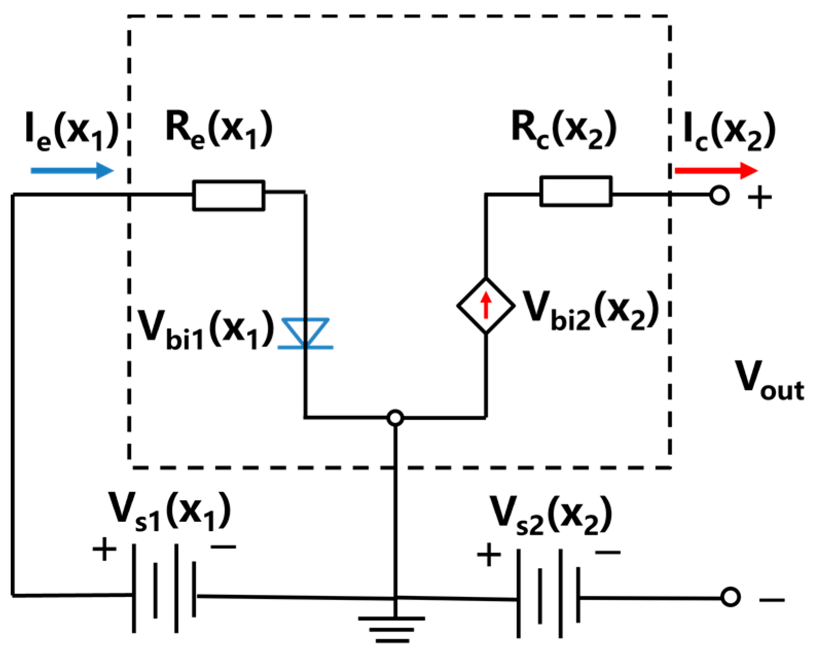
For bipolar thermoelectric transistors, the base–collector circuit can be considered as the output circuit. In this work, the early voltage effects of the emitter, base, and collector, as well as the contact resistance between the transistor and the electrodes, can be neglected. The corresponding equivalent DC circuit diagram is shown in Figure 2. The left side of the circuit diagram represents the equivalent circuit of the emitter–base junction. Vs1(x1) denotes the Seebeck voltage generated in the P1 region, serving as the external voltage at the emitter. Re(x1) represents the resistance of the P1 region of the emitter. Vbi1(x1) is assumed to be the forward voltage. On the right side of the circuit, the equivalent circuit of the base–collector junction is shown. Vs2(x2) signifies the Seebeck voltage generated in the P2 region, acting as the external voltage at the collector. Rc(x2) corresponds to the resistance of the P2 region of the collector. Vbi2(x2) is the voltage influenced by the emitter current Ie(x1). Furthermore, considering that the thickness of the base can be neglected compared to the emitter and collector and that it is fully depleted, the collector current Ic(x2) can be assumed to be equal to the emitter current Ie(x1).
According to the Kirchhoff’s law, the relationships among these electrical parameters can be expressed:
V e x 1 = V s 1 x 1 V b i 1 x 1 = I e x 1 R e x 1
V c x 2 = V b i 2 x 2 V s 2 x 2 = I c x 2 R c x 2
I e x 1 = I c x 2
R e x 1 = 1 p a 1 e μ p 1 × l x 1 w y h z
R c x 2 = 1 p a 2 e μ p 2 × l x 2 w y h z
where Ve(x1) is the emitter voltage, Vc(x2) is the collector voltage, and μp1 and μp2 are the hole mobility of the P1-type material (P1-Bi2Te3) and P2-type material (P2-Si), respectively. lx1 and lx2 represent the lengths of the P1-type and P2-type materials along the x direction, while wy and hz denote the lengths of the device in y and z directions, respectively, with values set to 1 μm. Sp2 is the Seebeck coefficient of the collector and m*p2 is the effective mass of the collector.
The output power of the transistor can be expressed as the product of the open-circuit voltage and the short-circuit current:
P o u t = I e x 1 × V o u t = I e x 1 × V c x 2 = I e x 1 × [ V b i 2 x 2 V s 2 x 2 ]

2.5. The Material Parameters of Thermoelectric Transistor

In this work, P1-Bi2Te3, N-Si, and P2-Si are selected as the emitter material, base material, and collector material, respectively. The material parameters of the thermoelectric transistor studied are listed in Table 1.

3. Results and Discussion

3.1. Temperature Distribution in Thermoelectric Transistor

3.1.1. Temperature Distribution in p-Type Bi2Te3

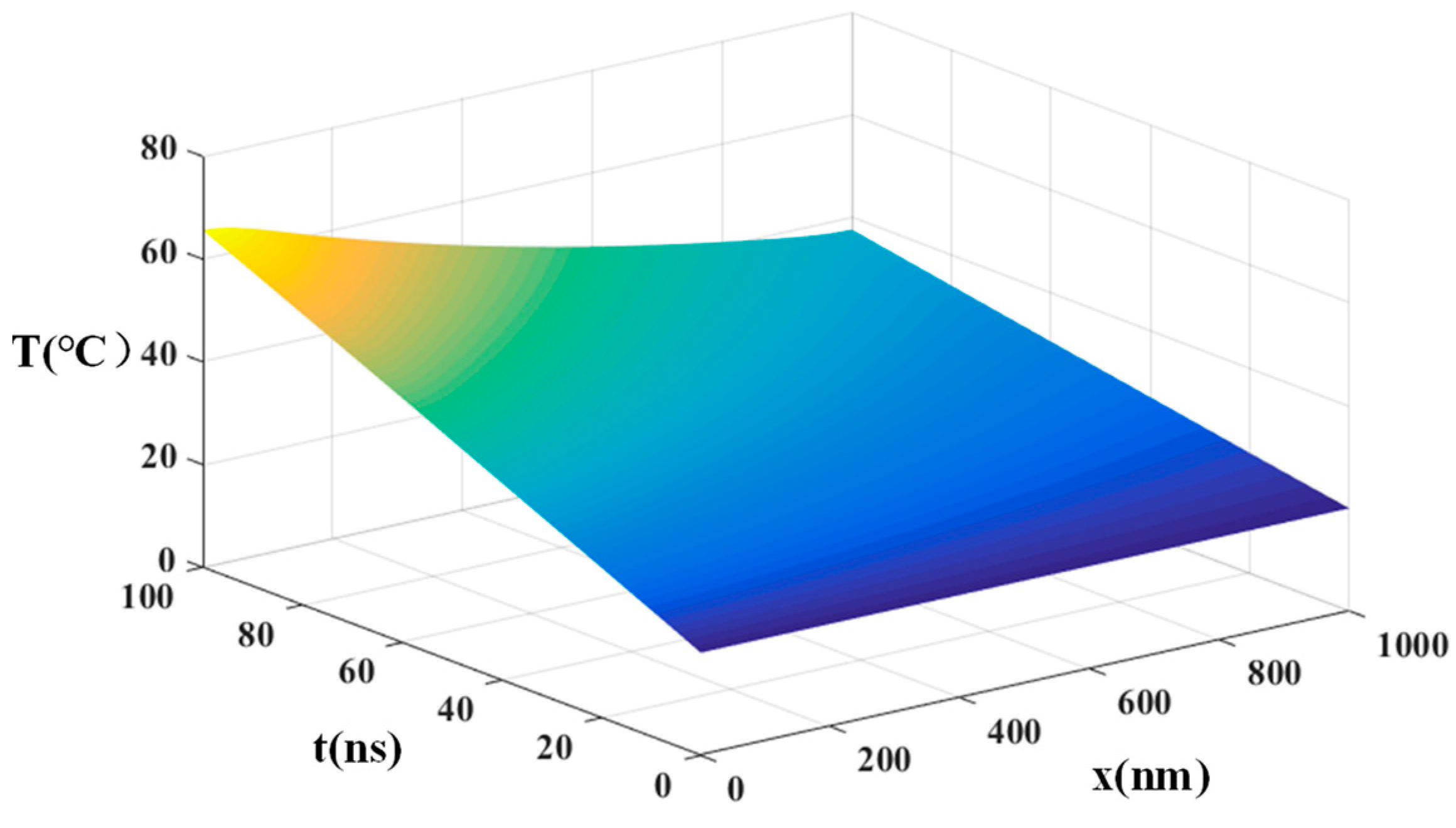
It is assumed that P1-Bi2Te3 is in the temperature of 20 °C. Under the condition of illuminating with an incident optical power of =3 × 10⁷(W·cm−2) for a duration of 100 ns, the temperature distribution within Bi2Te3 is obtained as shown in Figure 3.
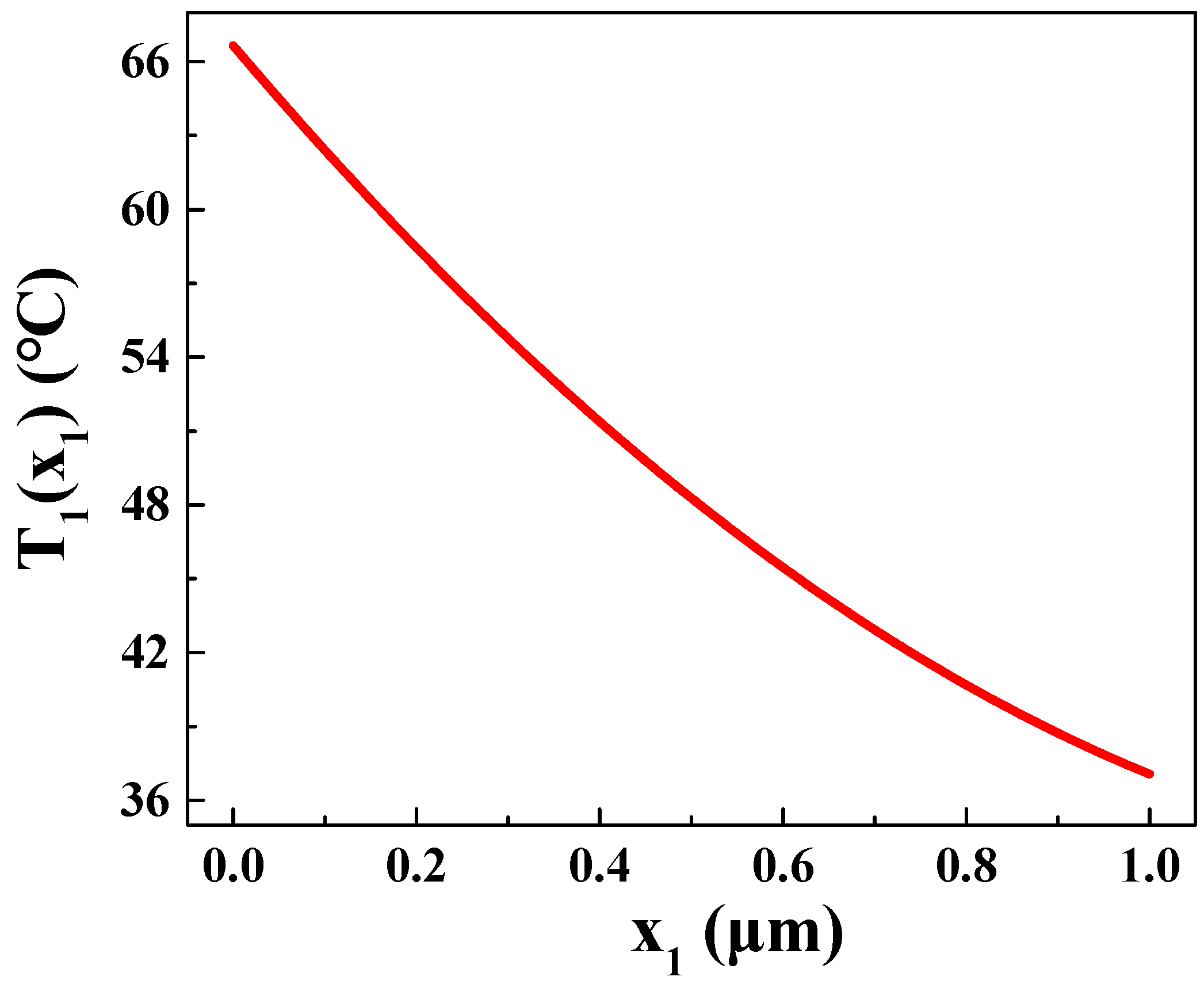
As depicted in Figure 3, it is apparent that, with an increase in laser irradiation time, the sample initiates heating from the irradiated surface at x = 0 μm. Subsequently, the heat gradually propagates throughout the entire device, and the lowest temperature is observed at x = 1 μm within P1 region. Figure 4 illustrates the temperature distribution in P1 region at T = 100 ns. Notably, after 100 ns of illumination, the temperature distribution in P1 region (Bi2Te3) exhibits a pattern of decreasing temperature as the distance from the laser increases. Specifically, at x = 0 μm, the temperature at 100 ns is Tb1 = 66.7 °C, whereas, at x = 1 μm, the temperature reaches its minimum value of Tb2 = 37 °C. By employing a quadratic function, the temperature variation T1(x1) in P1 region as a function of x can be obtained:
T 1 x 1 = 14.35 x 1 2 43.95 x 1 + 66.7

3.1.2. Temperature Distribution in p-Si

By solving the equations in MATLAB, the temperature distribution in P2 region (P2-Si) along the x direction can be obtained. After 100 ns, the temperature distribution is shown in Figure 5.
Based on Figure 5, it can be observed that the temperature distribution in P2-type region gradually decreases with increasing x. It is important to note that n-type region in this work is extremely thin. Therefore, the length of the n-type region along the x direction is assumed to be 0, implying that x1 = 1 μm coincides with x2 = 0 μm. At x2 = 0 μm, P2-Si exhibits the highest temperature, Ts1 = 37 °C, while, at x2 = 4 μm, p-Si reaches its lowest temperature, Ts2 = 20 °C. By fitting a curve to the data in the figure, a fitting function T2(x2) for the temperature distribution in P2-Si can be obtained:
T 2 x 2 = 0.1982 x 2 3 + 2.798 x 2 2 12.48 x 2 + 37

3.2. Hole Concentration Distribution within Thermoelectric Transistor

The thermoelectric transistor consists of P1-type region, N-type region, and P2-type region. As mentioned in the previous section, the temperature distribution along the x direction of the transistor is represented by Equations (45) and (46).
Considering that N-type region is assumed to be completely depleted, it contains no free mobile carriers. However, for both P1-type region and P2-type region, under the influence of temperature distribution, the holes migrate from the hot end to the cold end, leading to their accumulation at the cold end. By utilizing the calculation formula from the previous section, the concentration distribution of holes in P1-type region can be obtained:
p 1 x 1 = P a 1 × 6.429 × 10 13 x 1 1.532 × 10 4 3
From Figure 6, it is evident that p1(x1) increases with increasing x1. This indicates that the hole concentration in P1-type region gradually increases from the hot end to the cold end. Additionally, as Pa1 increases, p1(x1) also increases. Of note, p1(x1) = Pa1 is near the midpoint of the P1-type region (x10 = 0.501 μm), as shown in the dashed line in Figure 6. This is because the hole carriers in the P1-type region (Bi2Te3) redistribute only along the x direction, and the temperature difference is fixed. Therefore, the position x10 remains constant. As a result, it can be inferred that, for x1 < x10, p1(x1) < Pa1, and, for x10x1 ≤ 1 μm, p1(x1) ≥ Pa1, with equality only at x1 = x10.
Similarly, hole concentration distribution of P2-Si can be obtained:
p 2 x 2 = P a 2 × 5.773 × 10 4 1.858 × 10 8 × x 2 2 1.749 × 10 5 × x 2 + 39 3
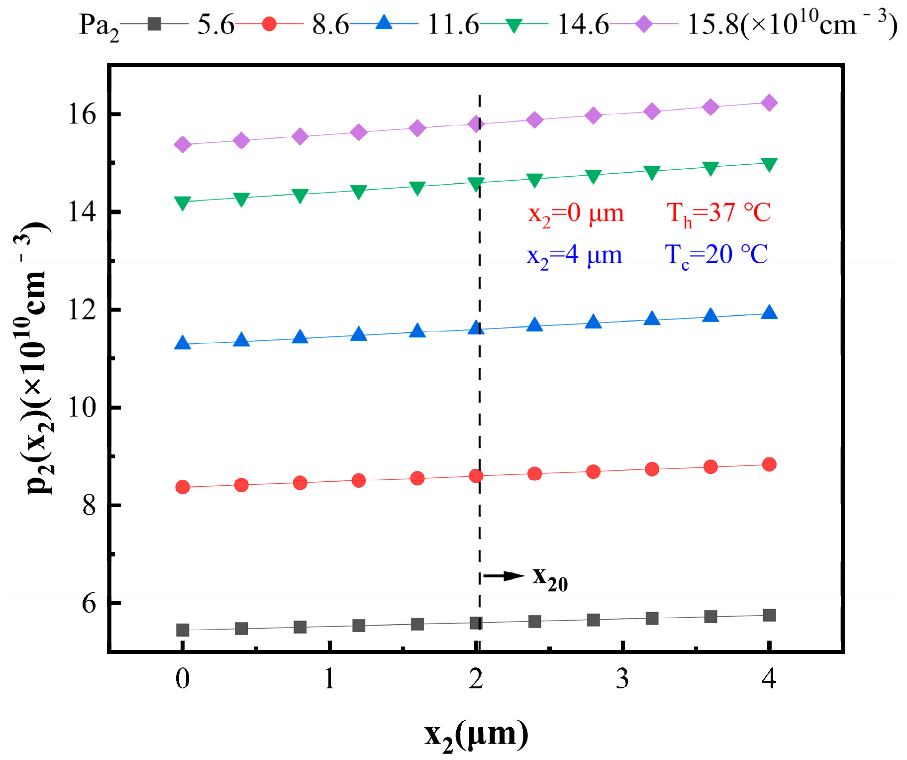
Figure 7 illustrates the variation in p2(x2) with respect to x2 for different Pa2. It can be observed that p2(x2) also increases with the increase in x2. Additionally, as Pa2 increases, p2(x2) increases. Similarly, at x20 = 2.009 μm, p2(x2) equals Pa2, as indicated by the dashed line in Figure 7. In other words, for 0 ≤x2 < x20 = 2.009 μm, Pa2 > p2(x2), and, for x20x2 ≤ 4 μm, p2(x2) ≥ Pa2, with equality only at x2 = x20.
Thus, it can be inferred that the Seebeck effect causes the redistribution of hole concentrations in both P1-type and P2-type regions, with holes diffusing from the hot end to the cold end. Consequently, the built-in voltage at both the P1–N junction and the N–P2 junction decreases from the cold end to the hot end. This unique characteristic enables such PNP heterojunctions to function as thermoelectric transistors. The emitter corresponds to the region with x10x1 ≤ 1 μm in the P1-type region, the base corresponds to the entire N-type region, and the collector corresponds to the region with 0 ≤ x2 < x20 = 2.009 μm in the P2-type region.

3.3. Operarion Conditions in Thermoelectric Transistor

3.3.1. Forward Bias of Emitter–Base Junction

When the entire thermoelectric transistor is at 20 °C, based on Equations (20)–(22), the required values for Pa1, Nd, and Pa2 can be determined:
P a 1 > p i 1 = 1.609 × 10 18 c m 3 , T = 20   ° C
N d > n i = 3.179 × 10 10 c m 3 , T = 20   ° C
P a 2 > p i 2 = 9.268 × 10 9 c m 3 , T = 20   ° C
For simplicity, their values are assumed to be 1.61 × 1018 cm−3, 3.2 × 1010 cm−3, and 1.0 × 1010 cm−3, respectively.
The temperature distribution T1(x1) and the temperature difference ΔT1(x1) for the emitter–base junction can be written:
T 1 x 1 = 14.35 x 1 2 43.95 x 1 + 66.7
T 1 x 1 = 14.35 x 1 2 43.95 x 1
x 1 0.501,1   μ m
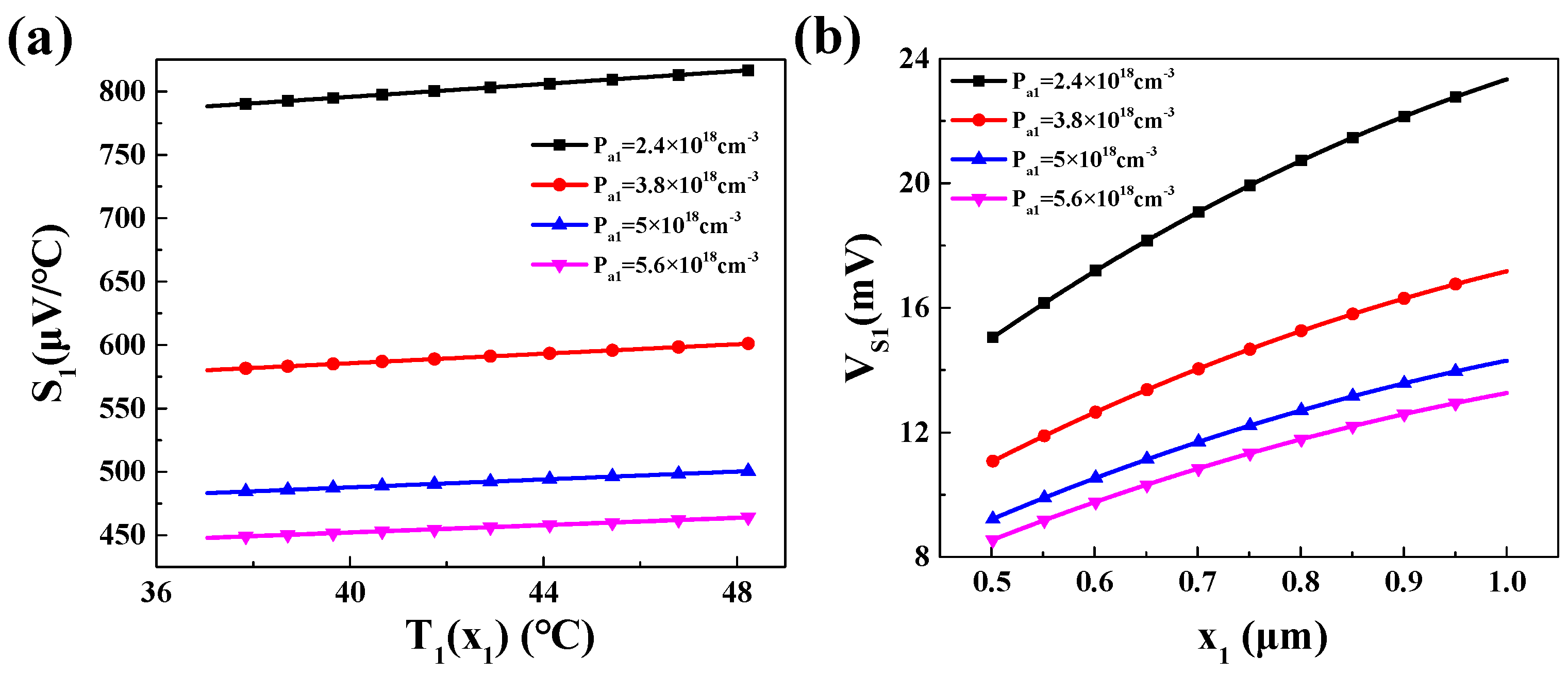
Under this temperature distribution, the calculated values for the Seebeck coefficient S1 and the Seebeck voltage Vs1 in P1 region are shown in Figure 8.
As shown in Figure 8, the Seebeck coefficient S1 of P1 region increases with the temperature T1(x1). Moreover, for different doping concentrations Pa1, the smaller doping concentration leads to a larger Seebeck coefficient. As for the Seebeck voltage Vs1, it exhibits a trend where it increases as the distance from the hot end (x1 = 0) increases due to the larger temperature difference.
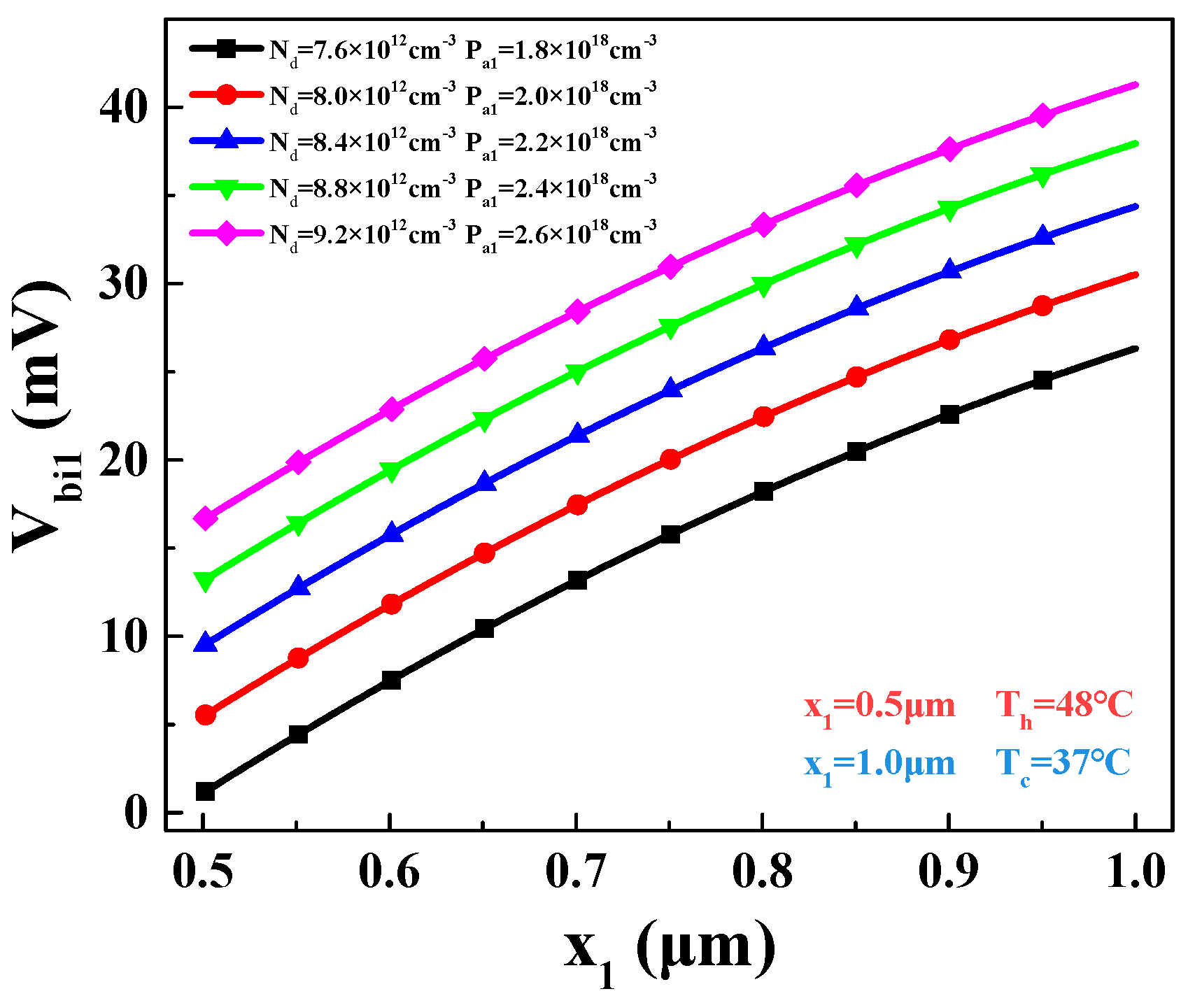
Additionally, the built-in voltage Vbi1 within P1-N region can be obtained, as shown in Figure 9.
Under different values of Pa1 and Nd, the built-in voltage increases with the increase in x1. This means that, as the temperature decreases, the built-in voltage increases. The increase is primarily attributed to the decrease in intrinsic carrier concentration with decreasing temperature.
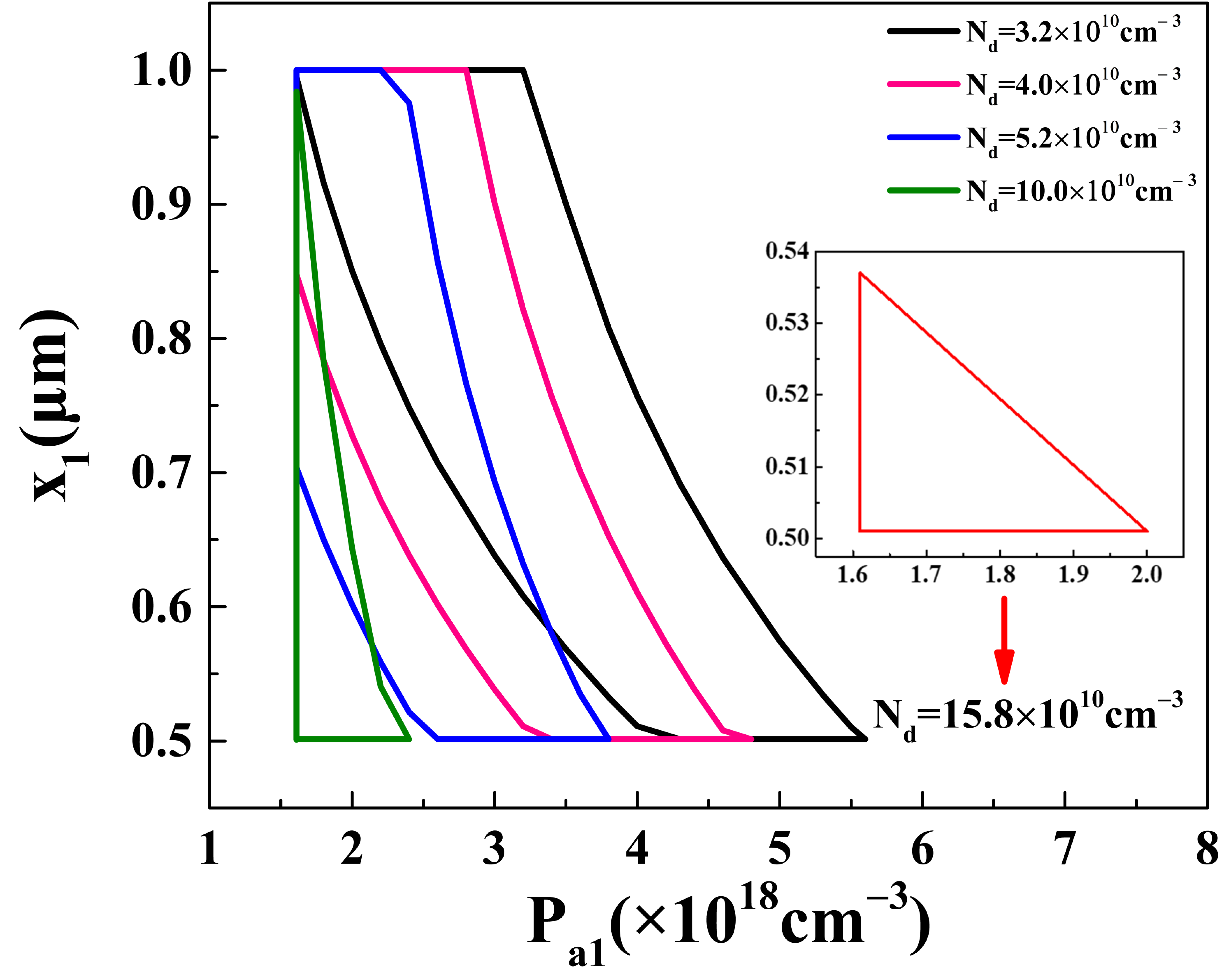
Based on Section 2.3.1, it can be concluded that achieving the forward bias and forward conduction of the emitter–base junction depends on three conditions: Vbi1(x1) > 0, Ve(x1) = Vs1(x1)–Vbi1(x1) > 0, and p1(x1) > Nd. These conditions are all influenced by Pa1, x1, and Nd. The appropriate concentration ranges for Pa1 and Nd are shown in Figure 10.
It can be observed that the suitable range for Nd is 3.2 × 1010 cm−3~15.8 × 1010 cm−3. As the range of Nd increases, the range of Pa1 decreases. When Nd is 3.2 × 1010 cm−3, the range of Pa1 is 1.61 × 1018 cm−3~5.6 × 1018 cm−3, as indicated by the black line. When Nd increases to 15.8 × 1010 cm−3, the range of Pa1 is only 1.61 × 1018 cm−3~2.0 × 1018 cm−3, as shown by the red line. This is because the built-in voltage Vbi1(x1) is positively correlated with Nd and Pa1. As Nd and Pa1 increase, Vbi1(x1) also increases, resulting in a smaller range of Pa1 for achieving Vs1(x1)–Vbi1(x1) > 0.
Additionally, it can be found that x1 also changes with Nd and Pa1. As Nd and Pa1 increase, the range of x1 gradually approaches 0.501 μm. This is because, at x1 = 1 μm, both Vbi1(x1) and Vs1(x1) reach their maximum values. However, in comparison to Vs1(x1), Vbi1(x1) increases at a faster rate as x1 increases. Therefore, it is relatively easier to achieve the operation conditions of the emitter–base junction at x1 = 0.501 μm. Thus, when Nd = 3.2 × 1010 cm−3, the maximum range of x1 is 0.608 μm to 1 μm. While Nd = 15.8 × 1010 cm−3, the maximum range of x1 is 0.501 μm to 0.537 μm. Therefore, the forward bias and forward conduction of the emitter–base junction can be achieved by adjusting the concentrations of Pa1 and Nd. Such a deigned doping concentration for P1-Bi2Te3 can be obtained directly by doping process, e.g., phosphorus as acceptor.

3.3.2. Reverse Bias of Base–Collector Junction

When a temperature gradient is applied in the base–collector junction, the temperature distribution equation T2(x2) and temperature difference ∆T2(x2) can be expressed as follows:
T 2 x 2 = 0.1982 x 2 3 + 2.798 x 2 2 12.48 x 2 + 37
T 2 x 2 = 0.1982 x 2 3 2.798 x 2 2 + 12.48 x 2 17
x 2 0,0.2   μ m
It should be noted that ∆T(x1) represents the temperature difference between the emitter and base, with a positive value. However, ∆T2(x2) represents the temperature difference between the collector and base, with a negative value. Therefore, Vs1(x1) has a positive value, while Vs2(x2) has a negative value.
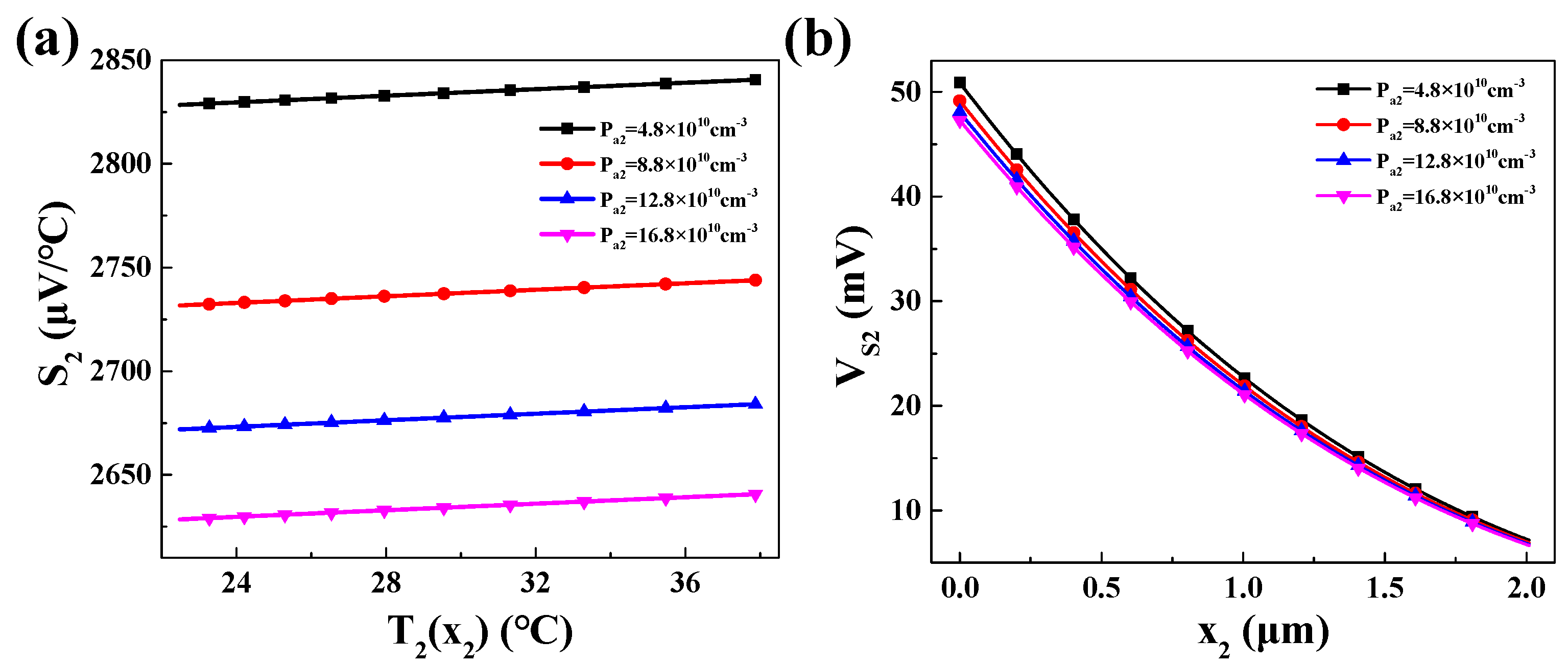
For P2 region, the values of the Seebeck coefficient S2 and the Seebeck voltage Vs2 are shown in Figure 11.
It can be observed that the Seebeck coefficient S2 of P2 region increases with temperature T2(x2). For different doping concentrations Pa2, a smaller doping concentration leads to a larger Seebeck coefficient. Regarding the Seebeck voltage Vs2, it exhibits a trend as the position approaches x2 = 0 (closer to the hot end) due to the increasing temperature difference.
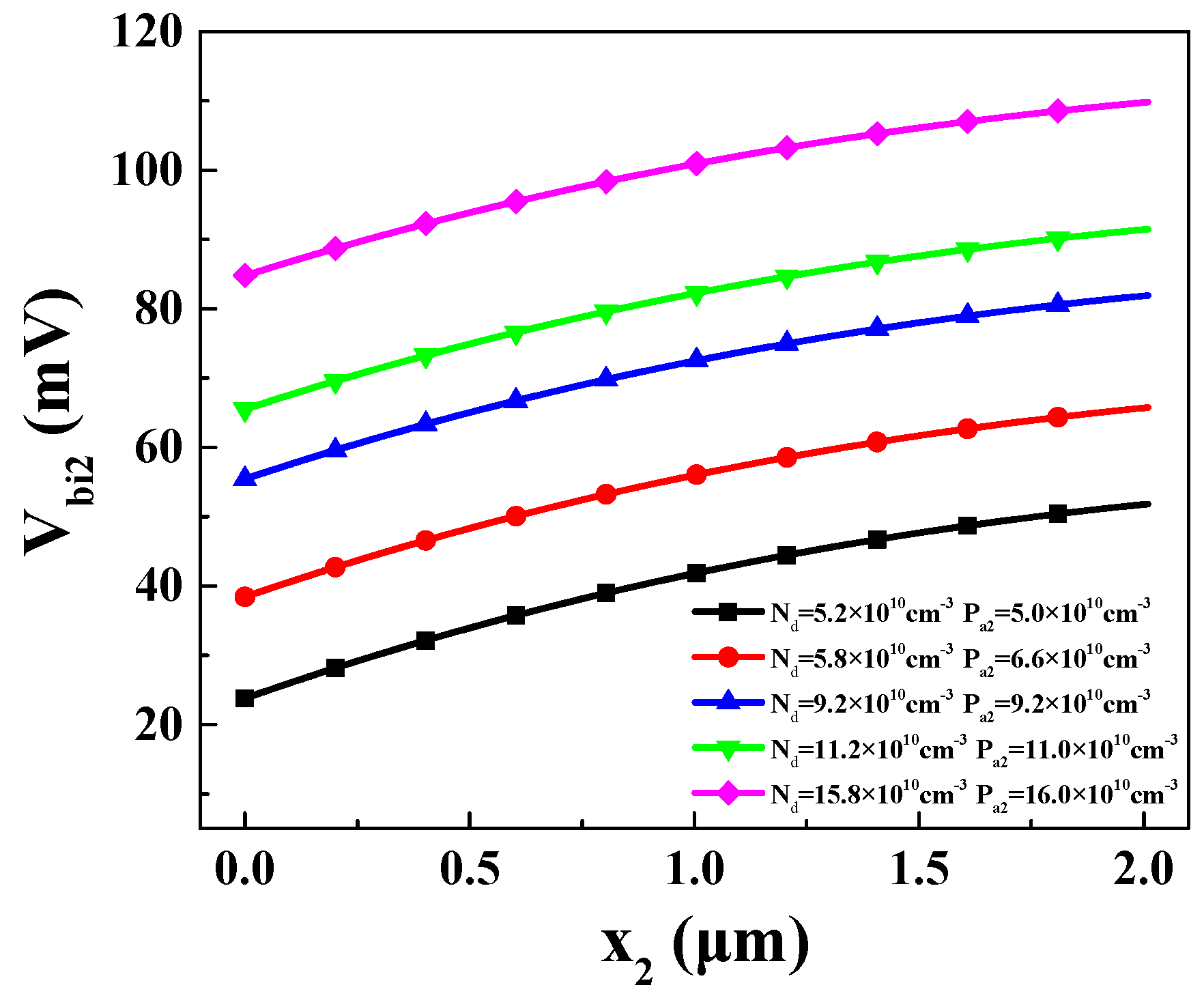
The built-in voltage Vbi2 in the N-P2 region is depicted in Figure 12. It can be found that the built-in voltage Vbi2 increases with increasing x2 at different values of Pa2 and Nd. In other words, as the temperature decreases, the built-in voltage increases. This increase primarily stems from the decrease in intrinsic charge carriers with decreasing temperature.
Based on Section 2.3.2, it can be concluded that achieving the forward bias and forward conduction of the emitter–base junction depends on three conditions: Vbi2(x2) > 0 and p2(x2) < Nd. These conditions are all influenced by Pa2, x2, and Nd. Therefore, the reverse bias in the base–collector junction can be achieved by adjusting the concentrations of Pa2 and Nd. The appropriate concentration ranges for Pa2 and Nd are shown in Figure 13.
Unlike the previous section, the range of Nd is from 5.2 × 1010 cm−3 to 15.8 × 1010 cm−3. It can be observed that, as Nd increases, the corresponding range of Pa2 also gradually increases. This is because higher values of Nd and Pa2 both lead to larger values of Vbi2(x2), making it easier to satisfy the reverse biasing condition Vbi2(x2) > 0.
To summarize, when Nd is within the range of 5.2 × 1010 cm−3 to 15.8 × 1010 cm−3, the thermoelectric transistor can be activated in the forward-active mode. The corresponding ranges of Pa1, Pa2, x1, and x2 are determined by the different values of Nd. By adjusting the concentrations of Pa1, Nd, and Pa2, the current can be generated in the thermoelectric transistor directly driven by the Seebeck effect.

3.4. Output Performance of Thermoelectric Transistor

It is evident that the output power of the transistor is primarily influenced by Pa1, Nd, Pa2, x1, and x2 based on Equation (44). Therefore, the impact of these parameters on the output power of the thermoelectric transistor is obtained in the following.

3.4.1. Impact of Nd on Output Power of Thermoelectric Transistor

Since the value of Nd directly affects the other four physical quantities, it is essential to initially examine the influence of Nd on the output power. Figure 14 illustrates the relationship between Nd and the maximum output power of the thermoelectric transistor.
It is evident that, as Nd gradually increases, Poutmax exhibits a trend of initially increasing and then decreasing. At Nd = 8.0 × 1010 cm−3, Poutmax reaches its maximum value of 0.7093 μW. It is important to note that different values of Nd correspond to various combinations of Pa1, Pa2, x1, and x2. Considering the multitude of possible parameter combinations, it is challenging to directly explain how Nd influences the output power. Therefore, a comprehensive enumeration of the parameters is necessary to identify the optimal solution, which, in this case, is Nd = 8.0 × 1010 cm−3 and Poutmax = 0.7093 μW.

3.4.2. Impact of Pa1 and x1 on Output Power of Thermoelectric Transistor

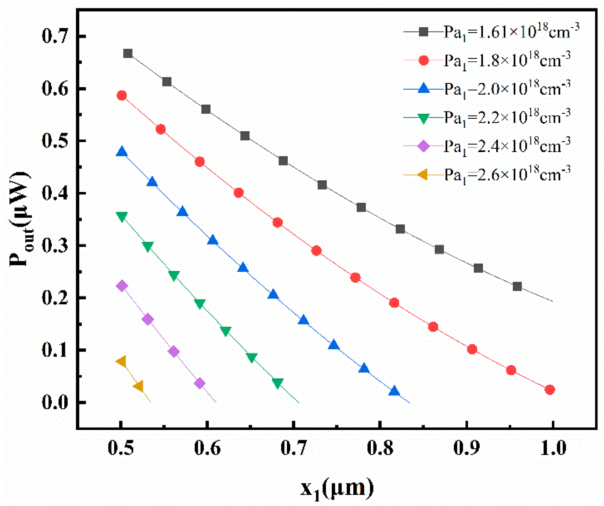
For Nd = 8.0 × 1010 cm−3, the range of Pa1 is from 1.61 × 1018 cm−3 to 2.6 × 1018 cm−3 and the range of Pa2 is from 1.0 × 1010 cm−3 to 8.2 × 1010 cm−3. Moreover, different values of Pa1 and Pa2 correspond to specific ranges of x1 and x2. Considering a fixed Pa2 value of 7.8 × 1010 cm−3 and x2 value of 0.4 μm, the relationship between output power (Pout) and the variations in Pa1 and x1 is illustrated in Figure 15.
It can be observed that the output power (Pout) increases as the concentration of Pa1 and x1 decrease. These results can be derived from Equation (58):
P o u t = I e x 1 × [ V b i 2 x 2 V s 2 x 2 ]
When Nd, Pa2, and x2 remain constant, the value of Pout is primarily influenced by Ie(x1):
I e x 1 = V s 1 x 1 V b i 1 x 1 R e x 1
At x1 = 1 μm, both Vbi1(x1) and Vs1(x1) reach their maximum values. However, compared to Vs1(x1), Vbi1(x1) increases more rapidly as x1 increases. Therefore, at x1 = 0.501 μm, Vs1(x1)–Vbi1(x1) reaches its maximum value. Thus, as x1 decreases within the range of x1 ∈ (0.501 μm, 1 μm), Pout increases. On the other hand, when other conditions remain unchanged, a larger Pa1 leads to a higher built-in voltage in the P1 region (Vs1(x1)–Vbi1(x1)). As a result, with an increase in Pa1, Pout decreases.

3.4.3. Impact of Pa2 and x2 on Output Power of Thermoelectric Transistor

The impact of Pa2 and x2 on the output power of the thermoelectric transistor is examined in the following when Pa1 = 1.61 × 1018 cm−3 and x1 = 0.508 μm. As shown in Figure 16, it can be observed that Pout increases as Pa2 increases and x2 decreases. Again, referring to the expression for Pout:
P o u t = I e x 1 × [ V b i 2 x 2 V s 2 x 2 ]
When Nd, Pa1, and x1 are constant, the value of Pout is mainly influenced by Vbi2(x2)–Vs2(x2). An increase in Pa2 leads to a higher value of Vbi2(x2), resulting in a larger difference between Vbi2(x2) and Vs2(x2). Consequently, as Pa2 increases, Pout also increases. On the other hand, when x2 increases, ∆T2(x2) decreases, resulting in a lower Vs2(x2) and higher Vbi2(x2). In this case, Vs2(x2) dominates the relationship and the value of Vbi2(x2)–Vs2(x2) decreases, leading to a decrease in Pout.

3.4.4. Transistor Structure: Optimization of Output Power Effects

As deduced from the above analysis, when Nd = 8.0 × 1010 cm−3, Pa1 = 1.61 × 1018 cm−3, Pa2 = 8.2 × 1010 cm−3, x1 = 0.508 μm, and x2 = 0 μm, the maximum output power of this designed thermoelectric transistor can reach 0.7093 μW.
If only Bi2Te3 is used without the thermoelectric transistor structure, the output power, can be calculated as 0.1442 μW. It can be observed that the designed thermoelectric transistor structure in this work results in an increase in the output power compared to a single thermoelectric material, with an improvement of 391.9%.

4. Conclusions

In this work, the temperature distribution and hole concentration distribution within the thermoelectric transistor is obtained through theoretical calculations. By considering the variation in the built-in voltage with temperature, the formation principle of the thermoelectric transistor is demonstrated. Subsequently, based on the operation conditions of the thermoelectric transistor, suitable doping concentrations of the emitter, base, and collector can be determined. Furthermore, the maximum output power of the thermoelectric transistor is obtained. The main conclusions drawn from this work are as follows:
(i)
The thermoelectric transistor, composed of P1-Bi2Te3, N-Si, and P2-Si, is directly irradiated by the laser. Under laser illumination and heat conduction, the temperature decreases from 66.7 °C to 20 °C, creating a temperature difference of 46.7 °C at the two ends of the thermoelectric transistor. As a result of the temperature difference, holes inside P1 and P2 regions migrate from the hot end to the far end, leading to increased hole concentration at the cold end.
(ii)
The operation conditions of the thermoelectric transistor under laser irradiation are investigated. Based on the corresponding conditions, suitable doping concentrations of the emitter, base, and collector can be determined. By adjusting these concentrations, the current can be produced in the thermoelectric transistor only driven by the Seebeck effect.
(iii)
The influence of these parameters on the output power of the thermoelectric transistor is also investigated. The maximum output power of the thermoelectric transistor is 0.7093 μW under a temperature difference of 46.7 °C, which is nearly quadrupling the performance compared to the single thermoelectric material structure.
(iv)
Importantly, the operation conditions of the thermoelectric transistor established in this work are applicable to other material systems. By adjusting the doping concentration within each region, current can be generated, ensuring that the forward-active mode is achieved. Therefore, this novel thermoelectric generator concept can significantly contribute to the advancement of the thermoelectric field. Moreover, the combination with transistor technology can expand the range of applications for thermoelectric generators.

Author Contributions

H.D.: conceptualization, methodology, formal analysis, writing—original draft; B.N.: conceptualization, methodology, formal analysis, writing—original draft; G.X.: investigation, supervision, conceptualization, principle proposal, funding acquisition. All authors have read and agreed to the published version of the manuscript.

Funding

This work was financially supported by The National Key Research and Development Program of China (Grant No. 2017YFF0204706), by The Fundamental Research Funds for the Central Universities (Grant No. FRF-MP-18-005, and FRFMP-19-005).

Institutional Review Board Statement

Not applicable.

Informed Consent Statement

Not applicable.

Data Availability Statement

The data presented in this study are available upon request from the corresponding author.

Conflicts of Interest

The authors declare no conflict of interest.

References

  1. Graus, W.H.J.; Voogt, M.; Worrell, E. International comparison of energy efficiency of fossil power generation. Energy Policy 2007, 35, 3936–3951. [Google Scholar] [CrossRef]
  2. Mallick, M.; Franke, L.; Rösch, A.G.; Geßwein, H.; Long, Z.; Eggeler, Y.M.; Lemmer, U. High Figure-of-Merit Telluride-Based Flexible Thermoelectric Films through Interfacial Modification via Millisecond Photonic-Curing for Fully Printed Thermoelectric Generators. Adv. Sci. 2022, 9, 2202411. [Google Scholar] [CrossRef] [PubMed]
  3. Shittu, S.; Li, G.-Q.; Zhao, X.-D.; Ma, X.-L. Review of thermoelectric geometry and structure optimization for performance enhancement. Appl. Energy 2020, 268, 115075. [Google Scholar] [CrossRef]
  4. Yang, F.; Wu, J.; Suwardi, A.; Zhao, Y.-S.; Laing, B.-Y.; Jiang, J.; Xu, J.-W.; Chi, D.-Z.; Hippalgaonkar, K.; Lu, J.-P.; et al. Gate-Tunable Polar Optical Phonon to Piezoelectric Scattering in Few-Layer Bi2O2Se for High-Performance Thermoelectrics. Adv. Mater. 2021, 4, 33. [Google Scholar]
  5. Wu, X.-M.; Gao, G.-Y.; Hu, L.; Qin, D. 2D Nb2SiTe4 and Nb2GeTe4: Promising thermoelectric figure of merit and gate-tunable thermoelectric performance. Nanotechnology 2021, 32, 245203. [Google Scholar] [CrossRef] [PubMed]
  6. Bejenari, I.; Kantser, V.; Balandin, A.A. Thermoelectric properties of electrically gated bismuth telluride nanowires. Phys. Rev. B. 2010, 81, 075316. [Google Scholar] [CrossRef] [Green Version]
  7. Qin, D.-L.; Pan, F.; Zhou, J.; Xu, Z.-B.; Deng, Y. High ZT and performance controllable thermoelectric devices based on electrically gated bismuth telluride thin films. Nano Energy 2021, 89, 106472. [Google Scholar] [CrossRef]
  8. Nan, B.; Xu, G.; Liu, W.-M.; Yang, Q.; Zhang, B.; Dong, Y.; Tie, J.; Guo, T.; Zhou, X. High thermoelectric performance of PNP abrupt heterostructures by independent regulation of the electrical conductivity and Seebeck coefficient. Mater. Today Commun. 2022, 31, 103343. [Google Scholar] [CrossRef]
  9. Nan, B.; Xu, G.; Yang, Q.; Zhang, B.; Zhou, X. Innovative design and optimized performance of thermoelectric transistor driven by the Seebeck effect. Energ. Convers. Manag. 2023, 283, 116880. [Google Scholar] [CrossRef]
  10. Hua, Z.J.; Zhang, X.; Tu, D.-W.; Wang, X.-Z.; Haung, N.-D. Learning to high-performance autofocus microscopy with laser illumination. Measurement 2023, 216, 112964. [Google Scholar] [CrossRef]
  11. Shi, Q.; Li, J.; Zhao, X.-W.; Chen, Y.-Y.; Zhang, F.-J.; Zhong, Y.; Ang, R. Comprehensive Insight into p-Type Bi2Te3-Based Thermoelectrics near Room Temperature. ACS Appl. Mater. Interfaces 2022, 14, 49425–49445. [Google Scholar] [CrossRef]
  12. Dashevsky, Z.; Skipidarov, S. Investigating the performance of bismuth-antimony telluride. In Novel Thermoelectric Materials and Device Design Concepts; Springer: Berlin/Heidelberg, Germany, 2019; pp. 3–21. [Google Scholar]
  13. Maksymuk, M.; Dzundza, B.; Matkivsky, O.; Horichok, I.; Shneck, R.; Dashevsky, Z. Development of the high performance thermoelectric unicouple based on Bi2Te3 compounds. J. Power Sources 2022, 530, 231301. [Google Scholar] [CrossRef]
  14. Li, L.-B.; Xu, H.-W.; Yang, H.-B.; Huang, S.-L.; Yang, H.; Li, Y.-A.; Zhang, Q.; Guo, Z.; Hu, H.-Y.; Sun, P.; et al. Design of Bi2Te3-based thermoelectric generator in a widely applicable system. J. Power Sources 2023, 559, 232661. [Google Scholar]
  15. Maksymuk, M.; Parashchuk, T.; Dzundza, B.; Nvkvruy, L.; Chernyak, L.; Dasheysky, Z. Highly efficient bismuth telluride-based thermoelectric microconverters. Mater. Today Energy 2021, 21, 100753. [Google Scholar] [CrossRef]
  16. Zhu, B.; Liu, X.-X.; Wang, Q.; Qiu, Y.; Shu, Z.; Guo, Z.-T.; Tong, Y.; Cui, J.; Gu, M.; He, J.-Q. Realizing record high performance in n-type Bi2Te3-based thermoelectric materials. Energy Environ. Sci. 2020, 13, 2106–2114. [Google Scholar] [CrossRef]
  17. Costa, L.D.F.; Silva, F.N.; Comin, C.H. Characterizing BJTs using the Early voltage in the forward active mode. Int. J. Circuit Theory App. 2018, 46, 978–986. [Google Scholar] [CrossRef]
  18. Bhattacharya, D.; Singh, R.; Holloway, P. Laser-target interactions during pulsed laser deposition of superconducting thin films. J. Appl. Phys. 1991, 70, 5433–5439. [Google Scholar] [CrossRef]
  19. Ge, Y.; He, K.; Xiao, L.-H.; Yuan, W.-Z.; Huang, S.-M. Geometric optimization for the thermoelectric generator with variable cross-section legs by coupling finite element method and optimization algorithm. Renew. Energy 2022, 183, 294–303. [Google Scholar] [CrossRef]
  20. Fu, D.; Levander, A.-X.; Zhang, R.; Ager, J.-W., III; Wu, J. Electrothermally driven current vortices in inhomogeneous bipolar semiconductors. Phys. Rev. B. 2011, 84, 045205. [Google Scholar] [CrossRef]
  21. Ravich, Y.I.; Pshenai-Severin, D. Thermoelectric figure of merit of a pn junction. Semiconductors 2001, 35, 1161–1165. [Google Scholar] [CrossRef]
  22. Lv, T.; Li, Z.-M.; Yang, Q.-X.; Benton, A.; Zheng, H.-T.; Xu, G.-Y. Synergistic regulation of electrical-thermal effect leading to an optimized thermoelectric performance in Co doping n-type Bi2(Te0.97Se0.03)3. Intermetallics 2020, 118, 106683. [Google Scholar] [CrossRef]
  23. Snyder, G.-J.; Toberer, E.-S. Complex thermoelectric materials. Nat. Mater. 2008, 7, 105–114. [Google Scholar] [CrossRef] [Green Version]
  24. Chavez, R.; Angst, S.; Hall, J.; Stoetzel, J.; Kessler, V.; Bitzer, L.; Maculewicz, F.; Benson, N.; Wiggers, H.; Wolf, D.; et al. Temperature Thermoelectric Device Concept Using Large Area PN Junctions. J. Electron. Mater. 2014, 43, 2376. [Google Scholar] [CrossRef]
  25. Neamen, D.-A. Microelectronics: Circuit Analysis and Design, 3rd ed.; McGraw-Hill: New York, NY, USA, 2007. [Google Scholar]
  26. Ahmad, F.; Singh, R.; Misra, P.-K.; Kumar, N.; Kumar, R.; Kumar, P. Fabrication of a p-n heterojunction using topological insulator Bi2Te3-Si and its annealing response. J. Electron Mater. 2018, 47, 6972–6983. [Google Scholar] [CrossRef]
  27. Zhou, J.; Li, X.-B.; Chen, G.; Yang, R.-G. Semiclassical model for thermoelectric transport in nanocomposites. Phys. Rev. B. 2010, 82, 115308. [Google Scholar] [CrossRef]
  28. Xu, G.-Y.; Ren, P.; Lin, T.; Wu, X.-F.; Zhang, Y.-H.; Niu, S.-T.; Bailey, T.P. Mechanism and application method to analyze the carrier scattering factor by electrical conductivity ratio based on thermoelectric property measurement. J. Appl. Phys. 2018, 123, 015101. [Google Scholar] [CrossRef]
  29. Chen, X.; Wang, Y.-C.; Ma, Y.-M.; Cui, T.; Zou, G.-T. Origin of the High Thermoelectric Performance in Si Nanowires: A First-Principle Study. J. Phys. Chem. C. 2009, 113, 14001–14005. [Google Scholar] [CrossRef]
  30. Yamasaka, S.; Watanabe, K.; Sakane, S.; Takeuch, S.; Sakai, A.; Sawano, K.; Nakamura, Y. Independent control of electrical and heat conduction by nanostructure designing for Si-based thermoelectric materials. Sci. Rep. 2016, 6, 22838. [Google Scholar] [CrossRef] [Green Version]
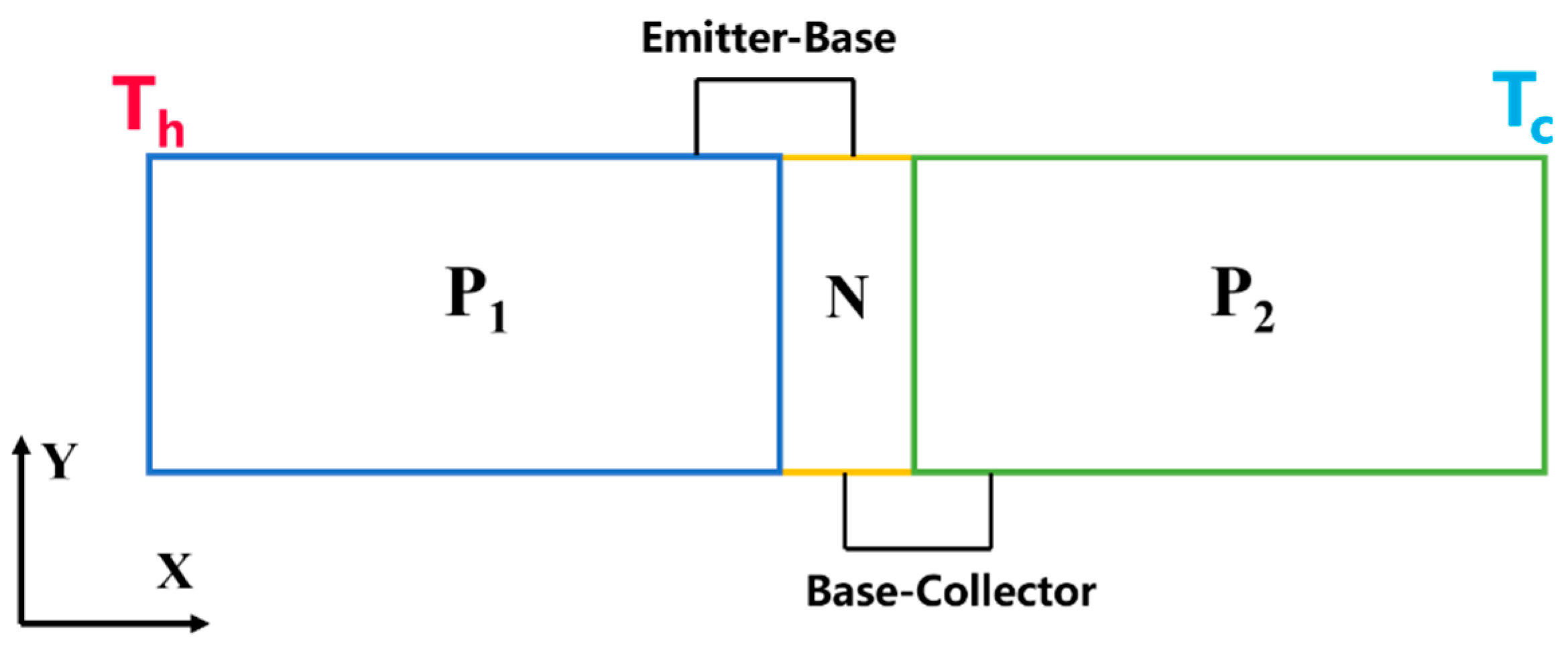
Figure 1. Diagram of thermoelectric transistor in X–Y plane.
Materials 16 05536 g001
Figure 2. Schematic diagram of equivalent circuit in thermoelectric transistor.
Materials 16 05536 g002
Figure 3. Temperature distribution of Bi2Te3 after laser irradiation with time t and x.
Materials 16 05536 g003
Figure 4. Temperature distribution in P1 region at t = 100 ns.
Materials 16 05536 g004
Figure 5. Temperature distribution in P2 region at t = 100 ns.
Materials 16 05536 g005
Figure 6. Relationship between p1(x1) and x1 at different hole concentrations.
Materials 16 05536 g006
Figure 7. Relationship between p2(x2) and x2 at different hole concentrations.
Materials 16 05536 g007
Figure 8. In the P1 region, under different doping concentrations Pa1: (a) the relationship between Seebeck coefficient S1 and temperature; (b) variation in Seebeck voltage Vs1 at different x1 positions.
Materials 16 05536 g008
Figure 9. Different values of built-in voltage in P1-N region on different x1.
Materials 16 05536 g009
Figure 10. Suitable range and corresponding x1 value of Pa1 that satisfies forward bias and forward conduction of emitter–base.
Materials 16 05536 g010
Figure 11. Under different doping concentrations Pa2: (a) the relationship between Seebeck coefficient S2 and temperature; (b) variation in Seebeck voltage Vs2 at different x2 positions.
Materials 16 05536 g011
Figure 12. Different values of built-in voltage in P2-N region on different x2.
Materials 16 05536 g012
Figure 13. Suitable range and corresponding x2 value of Pa2 that satisfies forward bias and forward conduction of emitter–base.
Materials 16 05536 g013
Figure 14. Variation in the maximum output power Pmax of the transistor with the value of Nd.
Materials 16 05536 g014
Figure 15. Variation in the maximum output power of transistor Pout with the values of Pa1 and x1.
Materials 16 05536 g015
Figure 16. Variation in the maximum output power of transistor Pout with the values of Pa2 and x2.
Materials 16 05536 g016
Table 1. Material parameters of thermoelectric transistor.
ParameterEmitterBaseCollectorRef.
Eg (eV)0.181.121.12[25,27]
m*/me1.46710.430.2601[28,29,30]
εr9011.711.7[6,25]
μp (cm2/V s)510-480[21,25]
Disclaimer/Publisher’s Note: The statements, opinions and data contained in all publications are solely those of the individual author(s) and contributor(s) and not of MDPI and/or the editor(s). MDPI and/or the editor(s) disclaim responsibility for any injury to people or property resulting from any ideas, methods, instructions or products referred to in the content.