
Reset-First and Multibit-Level Resistive-Switching Behavior of Lanthanum Nickel Oxide (LaNiO3−x) Thin Films

Abstract
:1. Introduction
2. Materials and Methods
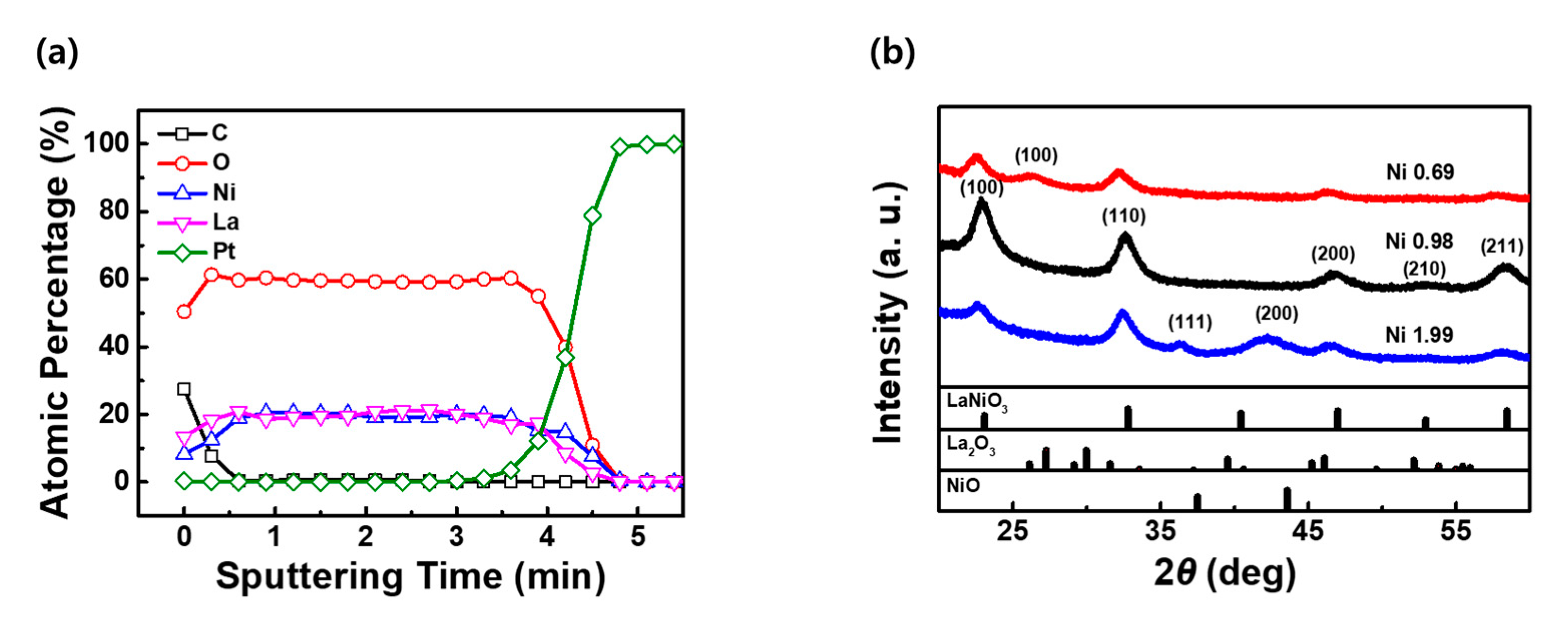
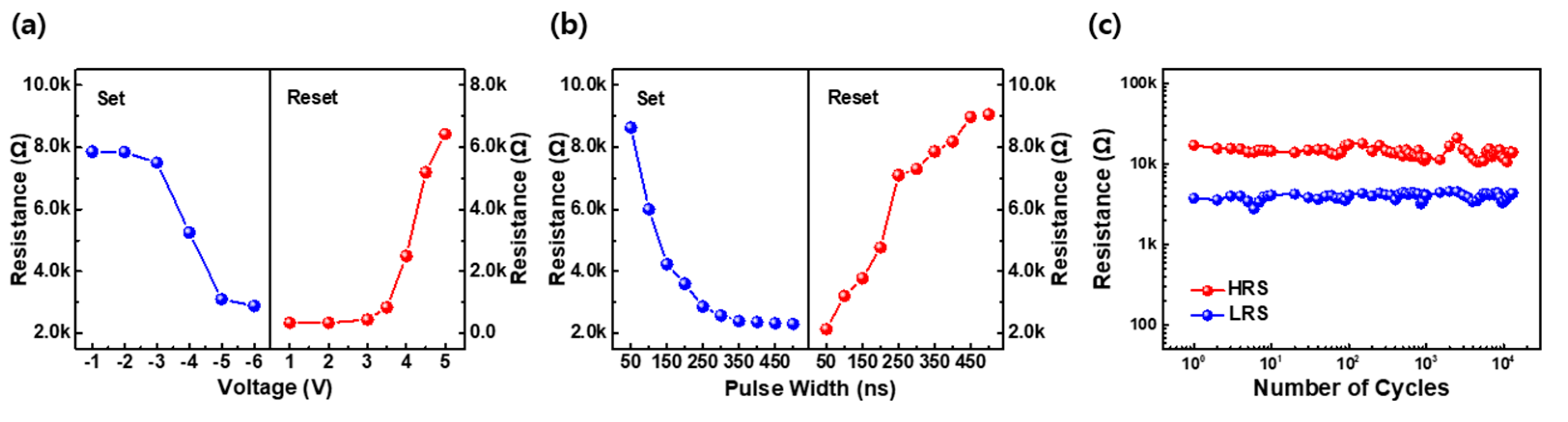
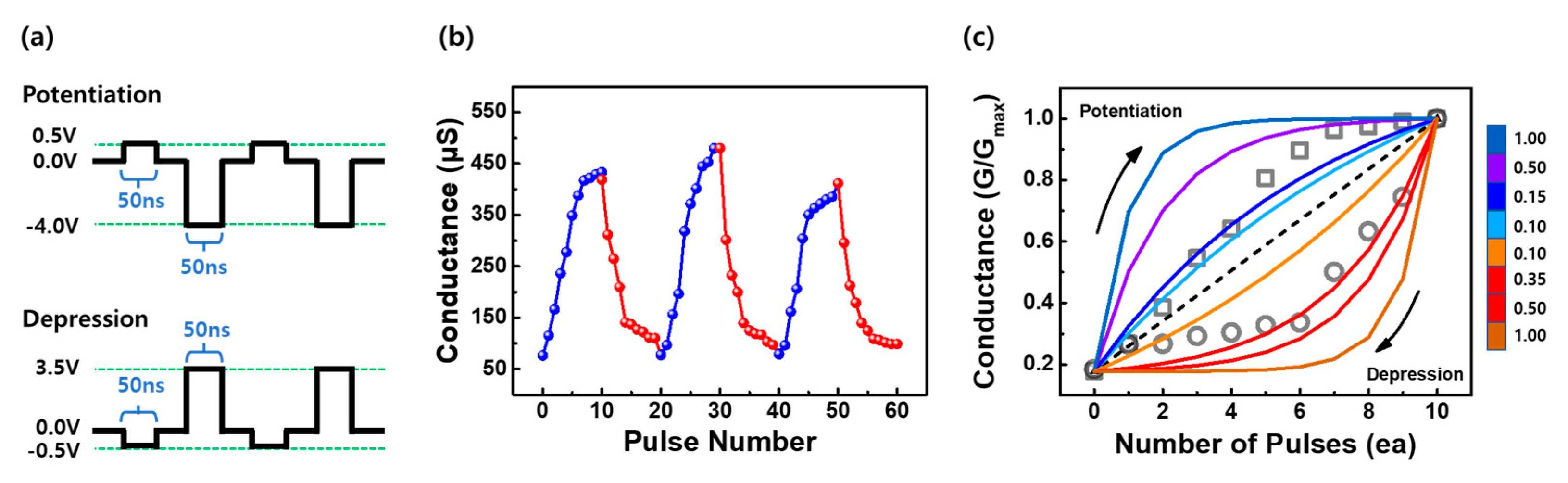
3. Results and Discussion
4. Conclusions
Supplementary Materials
Author Contributions
Funding
Institutional Review Board Statement
Informed Consent Statement
Data Availability Statement
Conflicts of Interest
References
- Catalano, S.; Gibert, M.; Fowlie, J.; Iniguez, J.; Triscone, J.-M.; Kreisel, J. Rare-earth nickelates RNiO3: Thin films and heterostructures. Rep. Prog. Phys. 2018, 81, 046501. [Google Scholar] [CrossRef] [Green Version]
- Alonso, J.A.; Martinez-Lope, M.J.; Casais, M.T.; Aranda, M.A.; Fernandez-Diaz, M.T. Metal-insulator transitions, structural and microstructural evolution of RNiO3 (R = Sm, Eu, Gd, Dy, Ho, Y) perovskites: Evidence for room-temperature charge disproportionation in monoclinic HoNiO3 and YNiO3. J. Am. Chem. Soc. 1999, 121, 4754–4762. [Google Scholar] [CrossRef]
- Mott, N.F. Metal-insulator transition. Rev. Mod. Phys. 1968, 40, 677. [Google Scholar] [CrossRef]
- Liu, J. Mott Transition and Electronic Structure in Complex Oxide Heterostructures. Ph.D. Thesis, University of Arkansas, Fayetteville, AR, USA, 2012. [Google Scholar]
- Wang, Y.; Kang, K.-M.; Kim, M.; Lee, H.-S.; Waser, R.; Wouters, D.; Dittmann, R.; Yang, J.J.; Park, H.-H. Mott-transition-based RRAM. Mater. Today 2019, 28, 63–80. [Google Scholar] [CrossRef]
- Dobin, A.Y.; Nikolaev, K.R.; Krivorotov, I.N.; Wentzcovitch, R.M.; Dahlberg, E.D.; Goldman, A.M. Electronic and crystal structure of fully strained LaNiO3 films. Phys. Rev. B 2003, 68, 113408. [Google Scholar] [CrossRef]
- Scherwitzl, R.; Gariglio, S.; Gabay, M.; Zubko, P.; Gibert, M.; Triscone, J.M. Metal-insulator transition in ultrathin LaNiO3 films. Phys. Rev. Lett. 2011, 106, 246403. [Google Scholar] [CrossRef] [Green Version]
- Wong, J.C.; Cheng, X.; Musavigharavi, P.; Xiang, F.; Hamilton, A.R.; Valanoor, N.; Sando, D. Understanding the Role of Defective Phases on the Conductivity Behavior of Strained Epitaxial LaNiO3 Thin Films. ACS Appl. Electron. Mater. 2022, 4, 1196–1205. [Google Scholar] [CrossRef]
- Sreedhar, K.; Honig, J.M.; Darwin, M.; McElfresh, M.; Shand, P.M.; Xu, J.; Crooker, B.C.; Spalek, J. Electronic properties of the metallic perovskite LaNiO3: Correlated behavior of 3d electrons. Phys. Rev. B Condens. Matter 1992, 46, 6382–6386. [Google Scholar] [CrossRef]
- Zhu, M.; Komissinskiy, P.; Radetinac, A.; Vafaee, M.; Wang, Z.; Alff, L. Effect of composition and strain on the electrical properties of LaNiO3 thin films. Appl. Phys. Lett. 2013, 103, 141902. [Google Scholar] [CrossRef]
- Chen, M.S.; Wu, T.B.; Wu, J.M. Effect of textured LaNiO3 electrode on the fatigue improvement of Pb(Zr0.53Ti0.47)O3 thin films. Appl. Phys. Lett. 1996, 68, 1430–1432. [Google Scholar] [CrossRef]
- Zhang, H.; Chen, X.; Wang, T.; Wang, F.; Shi, W. Structure and electrical properties of BiFeO3 thin films grown on LaNiO3 electrode by chemical solution deposition. J. Alloys Compd. 2010, 500, 46–48. [Google Scholar] [CrossRef]
- Wang, Y.G.; Tang, X.G.; Liu, Q.X.; Jiang, Y.P.; Feng, Z.Y. Ferroelectric and ferromagnetic properties of SrTi0.9Fe0.1O3−δ thin films. Solid State Commun. 2015, 202, 24–27. [Google Scholar] [CrossRef]
- Malashevich, A.; Ismail-Beigi, S. First-principles study of oxygen-deficient LaNiO3 structures. Phys. Rev. B 2015, 92, 144102. [Google Scholar] [CrossRef] [Green Version]
- Sanchez, R.; Causa, M.; Caneiro, A.; Butera, A.; Vallet-Regi, M.; Sayagués, M.; González-Calbet, J.; Garcia-Sanz, F.; Rivas, J. Metal-insulator transition in oxygen-deficient LaNiO3−x perovskites. Phys. Rev. B 1996, 54, 16574. [Google Scholar] [CrossRef] [PubMed]
- Abbate, M.; Zampieri, G.; Prado, F.; Caneiro, A.; Gonzalez-Calbet, J.M.; Vallet-Regi, M. Electronic structure and metal-insulator transition in LaNiO3−δ. Phys. Rev. B 2002, 65. [Google Scholar] [CrossRef]
- Wong, H.S.P.; Lee, H.-Y.; Yu, S.; Chen, Y.-S.; Wu, Y.; Chen, P.-S.; Lee, B.; Chen, F.T.; Tsai, M.-J. Metal–Oxide RRAM. Proc. IEEE 2012, 100, 1951–1970. [Google Scholar] [CrossRef]
- Zahoor, F.; Azni Zulkifli, T.Z.; Khanday, F.A. Resistive Random Access Memory (RRAM): An Overview of Materials, Switching Mechanism, Performance, Multilevel Cell (mlc) Storage, Modeling, and Applications. Nanoscale Res. Lett. 2020, 15, 90. [Google Scholar] [CrossRef] [PubMed]
- Meena, J.S.; Sze, S.M.; Chand, U.; Tseng, T.-Y. Overview of emerging nonvolatile memory technologies. Nano Scale Res. Lett. 2014, 9, 526. [Google Scholar] [CrossRef] [Green Version]
- Wang, L.; Yang, C.; Wen, J.; Gai, S. Emerging Nonvolatile Memories to Go Beyond Scaling Limits of Conventional CMOS Nanodevices. J. Nanomater. 2014, 2014, 927696. [Google Scholar] [CrossRef] [Green Version]
- Lee, G.H.; Hwang, S.; Yu, J.; Kim, H. Architecture and Process Integration Overview of 3D NAND Flash Technologies. Appl. Sci. 2021, 11, 6703. [Google Scholar] [CrossRef]
- Quan, X.-T.; Zhu, H.-C.; Cai, H.-T.; Zhang, J.-Q.; Wang, X.-J. Resistive Switching Behavior in Amorphous Aluminum Oxide Film Grown by Chemical Vapor Deposition. Chin. Phys. Lett. 2014, 31, 078101. [Google Scholar] [CrossRef]
- Rodrigues, A.; Santos, Y.; Rodrigues, C.; Macêdo, M. Al2O3 thin film multilayer structure for application in RRAM devices. Solid-State Electron. 2018, 149, 1–5. [Google Scholar] [CrossRef]
- Lin, Y.S.; Zeng, F.; Tang, S.G.; Liu, H.Y.; Chen, C.; Gao, S.; Wang, Y.G.; Pan, F. Resistive switching mechanisms relating to oxygen vacancies migration in both interfaces in Ti/HfOx/Pt memory devices. J. Appl. Phys. 2013, 113, 064510. [Google Scholar] [CrossRef]
- Raghavan, N.; Fantini, A.; Degraeve, R.; Roussel, P.J.; Goux, L.; Govoreanu, B.; Wouters, D.J.; Groeseneken, G.; Jurczak, M. Statistical insight into controlled forming and forming free stacks for HfOx RRAM. Microelectron. Eng. 2013, 109, 177–181. [Google Scholar] [CrossRef]
- Ku, B.; Abbas, Y.; Sokolov, A.S.; Choi, C. Interface engineering of ALD HfO2-based RRAM with Ar plasma treatment for reliable and uniform switching behaviors. J. Alloys Compd. 2018, 735, 1181–1188. [Google Scholar] [CrossRef]
- Lei, X.-Y.; Liu, H.-X.; Gao, H.-X.; Yang, H.-N.; Wang, G.-M.; Long, S.-B.; Ma, X.-H.; Liu, M. Resistive switching characteristics of Ti/ZrO2/Pt RRAM device. Chin. Phys. B 2014, 23, 117305. [Google Scholar] [CrossRef]
- Hussain, F.; Imran, M.; Khalil, R.A.; Sattar, M.A.; Niaz, N.A.; Rana, A.M.; Ismail, M.; Khera, E.A.; Rasheed, U.; Mumtaz, F. A first-principles study of Cu and Al doping in ZrO2 for RRAM device applications. Vacuum 2019, 168, 108842. [Google Scholar] [CrossRef]
- Wang, S.-Y.; Lee, D.-Y.; Huang, T.-Y.; Wu, J.-W.; Tseng, T.-Y. Controllable oxygen vacancies to enhance resistive switching performance in a ZrO2-based RRAM with embedded Mo layer. Nanotechnology 2010, 21, 495201. [Google Scholar] [CrossRef]
- Kim, T.; Son, H.; Kim, I.; Kim, J.; Lee, S.; Park, J.K.; Kwak, J.Y.; Park, J.; Jeong, Y. Reversible switching mode change in Ta2O5-based resistive switching memory (ReRAM). Sci. Rep. 2020, 10, 11247. [Google Scholar] [CrossRef]
- Sedghi, N.; Li, H.; Brunell, I.F.; Dawson, K.; Guo, Y.; Potter, R.J.; Gibbon, J.T.; Dhanak, V.R.; Zhang, W.D.; Zhang, J.F.; et al. Enhanced switching stability in Ta2O5 resistive RAM by fluorine doping. Appl. Phys. Lett. 2017, 111, 092904. [Google Scholar] [CrossRef] [Green Version]
- Xu, N.; Liu, L.; Sun, X.; Liu, X.; Han, D.; Wang, Y.; Han, R.; Kang, J.; Yu, B. Characteristics and mechanism of conduction/set process in TiN/ZnO/Pt resistance switching random-access memories. Appl. Phys. Lett. 2008, 92, 232112. [Google Scholar] [CrossRef]
- Simanjuntak, F.M.; Panda, D.; Wei, K.-H.; Tseng, T.-Y. Status and prospects of ZnO-based resistive switching memory devices. Nanoscale Res. Lett. 2016, 11, 368. [Google Scholar] [CrossRef] [PubMed] [Green Version]
- Asamitsu, A.; Tomioka, Y.; Kuwahara, H.; Tokura, Y. Current switching of resistive states in magnetoresistive manganites. Nature 1997, 388, 50. [Google Scholar] [CrossRef]
- Lashkare, S.; Chouhan, S.; Chavan, T.; Bhat, A.; Kumbhare, P.; Ganguly, U. PCMO RRAM for Integrate-and-Fire Neuron in Spiking Neural Networks. IEEE Electron Device Lett. 2018, 39, 484–487. [Google Scholar] [CrossRef]
- Panwar, N.; Ganguly, U. Variability assessment and mitigation by predictive programming in Pr0.7Ca0.3MnO3 based RRAM. In Proceedings of the 2015 73rd Annual Device Research Conference (DRC), Columbus, OH, USA, 21–24 June 2015; pp. 141–142. [Google Scholar]
- Kaith, P.; Garg, P.; Bera, A. Multilevel resistive switching in solution-processed CuFe2O4/TiO2 heterostructure. Appl. Phys. Lett. 2023, 122, 133301. [Google Scholar] [CrossRef]
- Wang, S.; Ning, X.; Hao, A.; Chen, R. Metal nanoparticles layer boosted resistive switching property in NiFe2O4-based memory devices. J. Alloys Compd. 2022, 908, 164569. [Google Scholar] [CrossRef]
- Rajarathinam, S.; Ganguly, U.; Venkataramani, N. Impact of oxygen partial pressure on resistive switching characteristics of PLD deposited ZnFe2O4 thin films for RRAM devices. Ceram. Int. 2022, 48, 7876–7884. [Google Scholar] [CrossRef]
- Ge, S.; Wang, Y.; Xiang, Z.; Cui, Y. Reset Voltage-Dependent Multilevel Resistive Switching Behavior in CsPb1–xBixI3 Perovskite-Based Memory Device. ACS Appl. Mater. Interfaces 2018, 10, 24620–24626. [Google Scholar] [CrossRef]
- Tian, Q.; Zhang, X.; Zhao, X.; Wang, Z.; Lin, Y.; Xu, H.; Liu, Y. Dual Buffer Layers for Developing Electrochemical Metallization Memory With Low Current and High Endurance. IEEE Electron Device Lett. 2021, 42, 308–311. [Google Scholar] [CrossRef]
- Mandal, S.; El-Amin, A.; Alexander, K.; Rajendran, B.; Jha, R. Novel synaptic memory device for neuromorphic computing. Sci. Rep. 2014, 4, 5333. [Google Scholar] [CrossRef] [Green Version]
- Park, S.; Noh, J.; Choo, M.L.; Sheri, A.M.; Chang, M.; Kim, Y.B.; Kim, C.J.; Jeon, M.; Lee, B.G.; Lee, B.H.; et al. Nanoscale RRAM-based synaptic electronics: Toward a neuromorphic computing device. Nanotechnology 2013, 24, 384009. [Google Scholar] [CrossRef] [PubMed]
- Shi, J.; Ha, S.D.; Zhou, Y.; Schoofs, F.; Ramanathan, S. A correlated nickelate synaptic transistor. Nat. Commun. 2013, 4, 2676. [Google Scholar] [CrossRef] [PubMed] [Green Version]
- Safi, I. Recent aspects concerning DC reactive magnetron sputtering of thin films: A review. Surf. Coat. Technol. 2000, 127, 203–218. [Google Scholar] [CrossRef]
- Davidse, P.; Maissel, L. Dielectric thin films through rf sputtering. J. Appl. Phys. 1966, 37, 574–579. [Google Scholar] [CrossRef]
- Vossen, J. Control of film properties by rf-sputtering techniques. J. Vac. Sci. Technol. 1971, 8, S12–S30. [Google Scholar] [CrossRef]
- Effects of applied electrical field on electronic structures in LaNiO3 conductive metallic oxide film: An optical spectroscopic study. Appl. Phys. Lett. 2010, 97. [CrossRef]
- Zhou, Q.; Cannata, J.M.; Meyer, R.J.; Van Tol, D.J.; Tadigadapa, S.; Hughes, W.J.; Shung, K.K.; Trolier-McKinstry, S. Fabrication and characterization of micromachined high-frequency tonpilz transducers derived by PZT thick films. IEEE Trans. Ultrason. Ferroelectr. Freq. Control. 2005, 52, 350–357. [Google Scholar] [CrossRef]
- Yan, H.; Zhang, D.; Xu, J.; Lu, Y.; Liu, Y.; Qiu, K.; Zhang, Y.; Luo, Y. Solution growth of NiO nanosheets supported on Ni foam as high-performance electrodes for supercapacitors. Nanoscale Res. Lett. 2014, 9, 1–7. [Google Scholar] [CrossRef] [Green Version]
- Qiao, L.; Bi, X. Direct observation of Ni3+ and Ni2+ in correlated LaNiO3−δ films. EPL (Europhys. Lett.) 2011, 93, 57002. [Google Scholar] [CrossRef]
- Qiao, L.; Bi, X. Direct observation of oxygen vacancy and its effect on the microstructure, electronic and transport properties of sputtered LaNiO3−δ films on Si substrates. Thin Solid Films 2010, 519, 943–946. [Google Scholar] [CrossRef]
- Mickevičius, S.; Grebinskij, S.; Bondarenka, V.; Vengalis, B.; Šliužienė, K.; Orlowski, B.A.; Osinniy, V.; Drube, W. Investigation of epitaxial LaNiO3−x thin films by high-energy XPS. J. Alloys Compd. 2006, 423, 107–111. [Google Scholar] [CrossRef] [Green Version]
- Misra, D.; Kundu, T.K. Oxygen vacancy induced metal-insulator transition in LaNiO3. Eur. Phys. J. B 2016, 89. [Google Scholar] [CrossRef]
- Bagdzevicius, S.; Maas, K.; Boudard, M.; Burriel, M. Interface-type resistive switching in perovskite materials. J. Electroceramics 2017, 39, 157–184. [Google Scholar] [CrossRef]
- Moon, K.; Lim, S.; Park, J.; Sung, C.; Oh, S.; Woo, J.; Lee, J.; Hwang, H. RRAM-based synapse devices for neuromorphic systems. Faraday Discuss. 2019, 213, 421–451. [Google Scholar] [CrossRef]
- Choi, J.-M.; Park, E.-J.; Woo, J.-J.; Kwon, K.-W. A highly linear neuromorphic synaptic device based on regulated charge trap/detrap. IEEE Electron Device Lett. 2019, 40, 1848–1851. [Google Scholar] [CrossRef]
- Chen, P.-Y.; Lin, B.; Wang, I.-T.; Hou, T.-H.; Ye, J.; Vrudhula, S.; Seo, J.-S.; Cao, Y.; Yu, S. Mitigating effects of non-ideal synaptic device characteristics for on-chip learning. In Proceedings of the 2015 IEEE/ACM International Conference on Computer-Aided Design (ICCAD), Austin, TX, USA, 2–6 November 2015; pp. 194–199. [Google Scholar]
- Li, Y.; Xuan, Z.; Lu, J.; Wang, Z.; Zhang, X.; Wu, Z.; Wang, Y.; Xu, H.; Dou, C.; Kang, Y.; et al. One Transistor One Electrolyte-Gated Transistor Based Spiking Neural Network for Power-Efficient Neuromorphic Computing System. Adv. Funct. Mater. 2021, 31, 2100042. [Google Scholar] [CrossRef]
- Wu, W.; Wu, H.; Gao, B.; Yao, P.; Zhang, X.; Peng, X.; Yu, S.; Qian, H. A methodology to improve linearity of analog RRAM for neuromorphic computing. In Proceedings of the 2018 IEEE Symposium on VLSI Technology, Honolulu, HI, USA, 18–22 June 2018; pp. 103–104. [Google Scholar]


Disclaimer/Publisher’s Note: The statements, opinions and data contained in all publications are solely those of the individual author(s) and contributor(s) and not of MDPI and/or the editor(s). MDPI and/or the editor(s) disclaim responsibility for any injury to people or property resulting from any ideas, methods, instructions or products referred to in the content. |
© 2023 by the authors. Licensee MDPI, Basel, Switzerland. This article is an open access article distributed under the terms and conditions of the Creative Commons Attribution (CC BY) license (https://creativecommons.org/licenses/by/4.0/).
Share and Cite
Kim, D.; Lee, J.; Kim, J.; Sohn, H. Reset-First and Multibit-Level Resistive-Switching Behavior of Lanthanum Nickel Oxide (LaNiO3−x) Thin Films. Materials 2023, 16, 4992. https://doi.org/10.3390/ma16144992
Kim D, Lee J, Kim J, Sohn H. Reset-First and Multibit-Level Resistive-Switching Behavior of Lanthanum Nickel Oxide (LaNiO3−x) Thin Films. Materials. 2023; 16(14):4992. https://doi.org/10.3390/ma16144992
Chicago/Turabian StyleKim, Daewoo, Jeongwoo Lee, Jaeyeon Kim, and Hyunchul Sohn. 2023. "Reset-First and Multibit-Level Resistive-Switching Behavior of Lanthanum Nickel Oxide (LaNiO3−x) Thin Films" Materials 16, no. 14: 4992. https://doi.org/10.3390/ma16144992
APA StyleKim, D., Lee, J., Kim, J., & Sohn, H. (2023). Reset-First and Multibit-Level Resistive-Switching Behavior of Lanthanum Nickel Oxide (LaNiO3−x) Thin Films. Materials, 16(14), 4992. https://doi.org/10.3390/ma16144992