
Crystallographic Texture and Substructural Phenomena in 316 Stainless Steel Printed by Selective Laser Melting


 ,
, 
 , and
, and 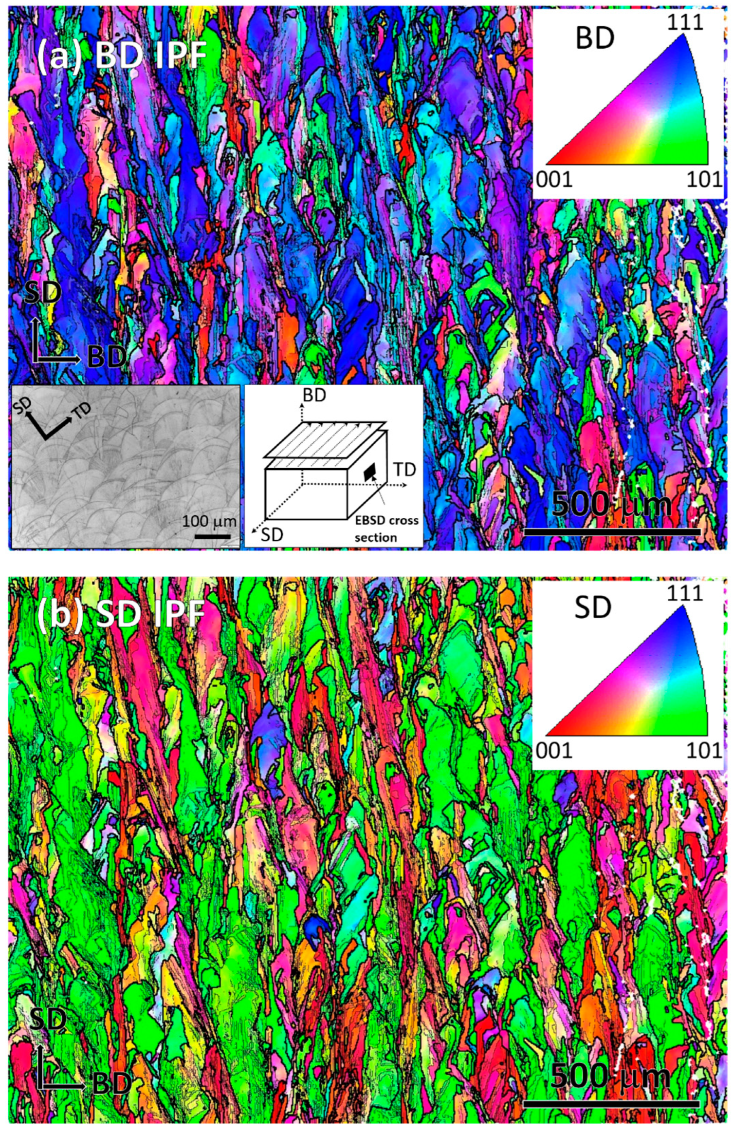
Abstract
1. Introduction
2. Materials and Methods
3. Results and Discussion
3.1. Structural Symmetry and Crystallographic Texture
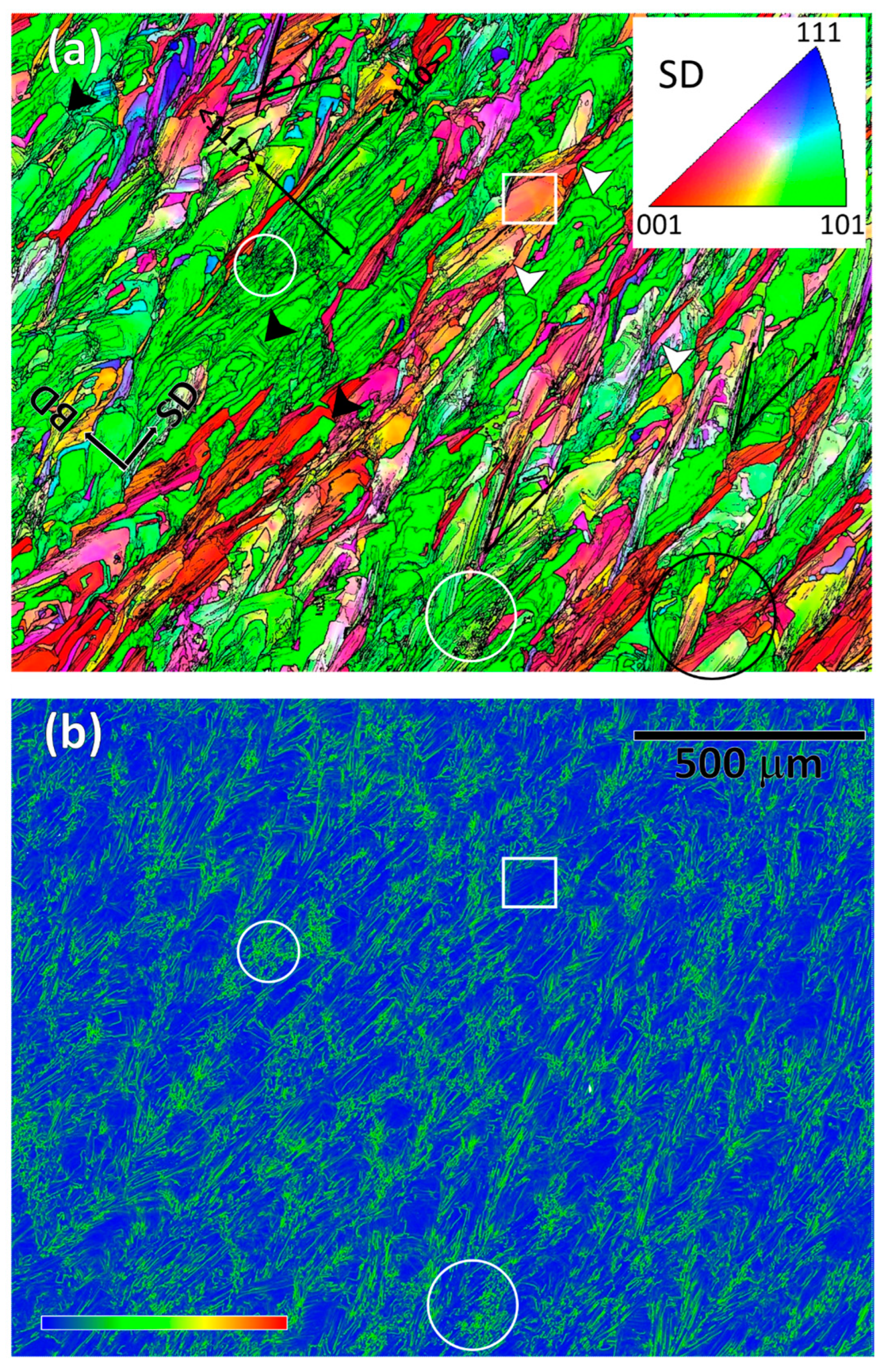
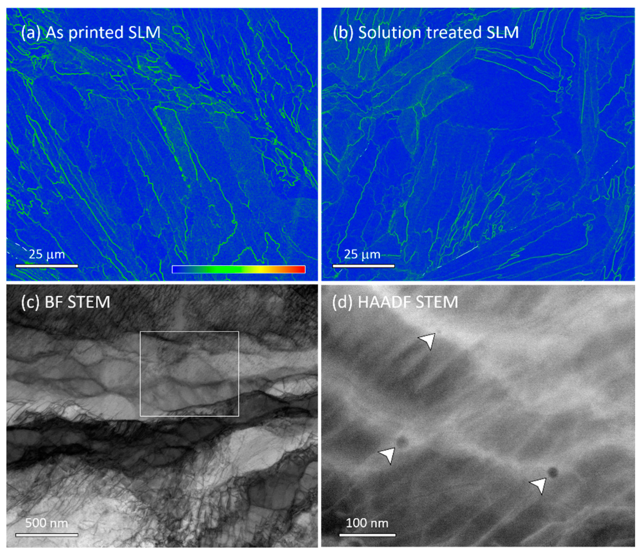
3.2. Substructural Features
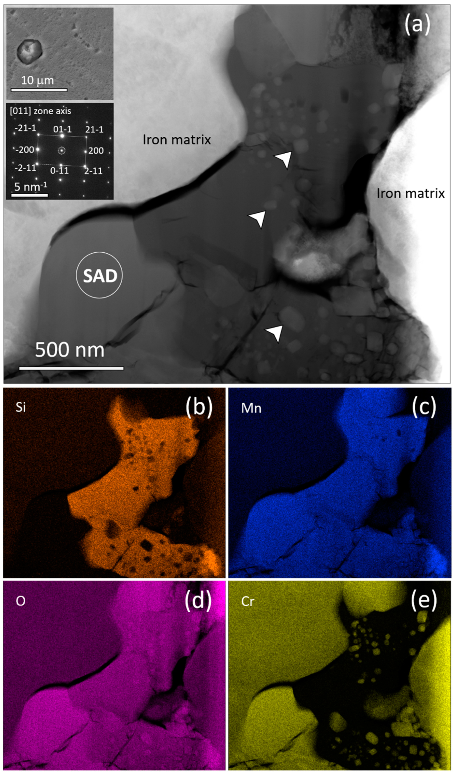
3.3. Solution Treatment Structures
4. Conclusions
- SLM-printed material possesses an asymmetric crystallographic texture and material structure. The microstructure has a distinctive structural morphology along the orthogonal axes of the sample, and develops crystallographic textures in SD ||<101> and BD ||<111>.
- Heterogenous distributions of misorientation boundaries and stored energy were found throughout the SLM-printed structures. Twin boundary formation was not observed in either the as-printed or solution-annealed samples.
- In the as-printed structures, the typical straight misorientation boundaries were characterized as being non-crystallographic. The boundaries maintained general alignment with the SD within an angular range, irrespective of the matrix’s crystal orientation, although there were occasional coincidences with crystal plane traces.
- The high-angle boundaries in the SLM substructures underwent thermal restoration, which was activated by the heat originating from the printing of the subsequent layer. Pinning by the nano inclusions hindered classical recrystallization, and thus, prevented the formation of a defect-free annealing structure, even after 4 h of solution treatment at 1050 °C.
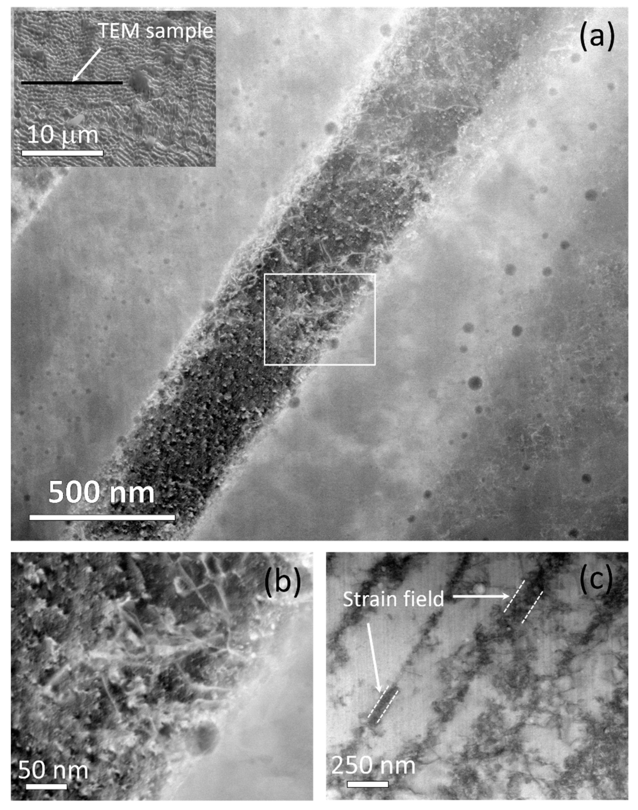
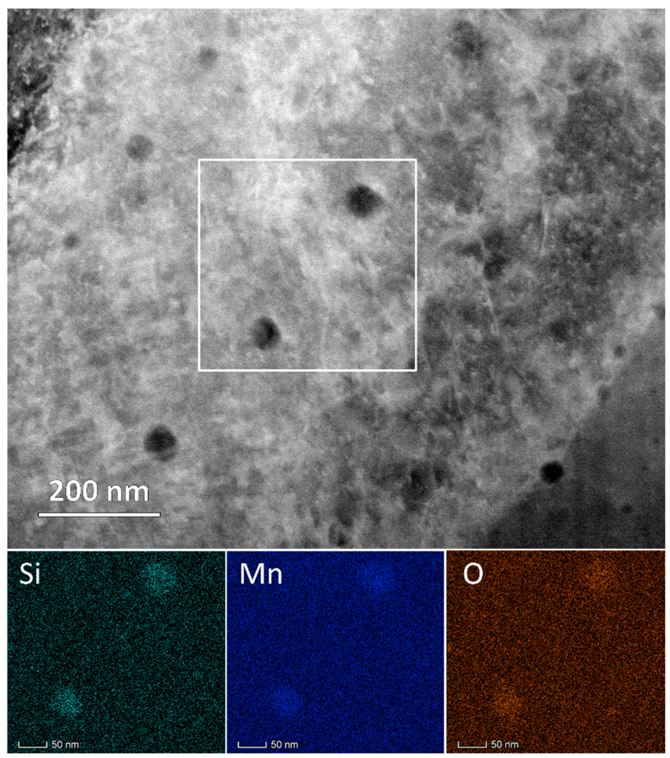
- A nano-scale lamellar structure with a width of 500 ± 200 nm formed homogeneously throughout the printed material. Depending on the orientation, the structures appeared with cellular or columnar morphologies in SEM and TEM images. Their boundaries contained dense dislocation structures tangled with fine amorphous inclusions containing Mn, Si and O. Cr was not found above the limit of detection in the inclusions. Hence, Cr remains in the matrix to provide the stainless properties.
- Some degree of dissociation of the dislocation boundaries occurred during the solution treatment, but the overall refined structures were retained. Additionally, inclusions with a size of 2–4 μm formed, consisting of composite structures and chemical distributions. These inclusions can have detrimental effects on the localized corrosion resistance of the alloy.
Author Contributions
Funding
Institutional Review Board Statement
Informed Consent Statement
Data Availability Statement
Acknowledgments
Conflicts of Interest
References
- Meiners, W.; Wissenbach, K.; Gasser, A. Shaped Body Especially Prototype or Replacement Part Production. DE Patent DE19649865C1, 12 February 1998. [Google Scholar]
- DebRoy, T.; Wei, H.L.; Zuback, J.S.; Mukherjee, T.; Elmer, J.W.; Milewski, J.O.; Beese, A.M.; Wilson-Heid, A.; De, A.; Zhang, W. Additive manufacturing of metallic components—Process, structure and properties. Prog. Mater. Sci. 2018, 92, 112–224. [Google Scholar] [CrossRef]
- Harun, W.; Kamariah, M.; Muhamad, N.; Ghani, S.; Ahmad, F.; Mohamed, Z. A review of powder additive manufacturing processes for metallic biomaterials. Powder Technol. 2018, 327, 128–151. [Google Scholar] [CrossRef]
- Song, B.; Dong, S.; Deng, S.; Liao, H.; Coddet, C. Microstructure and tensile properties of iron parts fabricated by selective laser melting. Opt. Laser Technol. 2014, 56, 451–460. [Google Scholar] [CrossRef]
- Olakanmi, E.O.; Cochrane, R.F.; Dalgarno, K.W. A review on selective laser sintering/melting (SLS/SLM) of aluminium alloy powders: Processing, microstructure, and properties. Prog. Mater. Sci. 2015, 74, 401–477. [Google Scholar] [CrossRef]
- Liu, Z.; Zhang, D.; Sing, S.; Chua, C.; Loh, L. Interfacial characterization of SLM parts in multi-material processing: Metallurgical diffusion between 316L stainless steel and C18400 copper alloy. Mater. Charact. 2014, 94, 116–125. [Google Scholar] [CrossRef]
- Shi, R.; Khairallah, S.A.; Roehling, T.T.; Heo, T.W.; McKeown, J.T.; Matthews, M.J. Microstructural control in metal laser powder bed fusion additive manufacturing using laser beam shaping strategy. Acta Mater. 2020, 184, 284–305. [Google Scholar] [CrossRef]
- Mower, T.M.; Long, M.J. Mechanical behavior of additive manufactured, powder-bed laser-fused materials. Mater. Sci. Eng. A 2016, 651, 198–213. [Google Scholar] [CrossRef]
- Maconachie, T.; Leary, M.; Lozanovski, B.; Zhang, X.; Qian, M.; Faruque, O.; Brandt, M. SLM lattice structures: Properties, performance, applications and challenges. Mater. Des. 2019, 183, 108137. [Google Scholar] [CrossRef]
- Maskery, I.; Aremu, A.; Simonelli, M.; Tuck, C.; Wildman, R.; Ashcroft, I.; Hague, R. Mechanical properties of Ti-6Al-4V selectively laser melted parts with body-centred-cubic lattices of varying cell size. Exp. Mech. 2015, 55, 1261–1272. [Google Scholar] [CrossRef]
- Maskery, I.; Aboulkhair, N.; Aremu, A.; Tuck, C.; Ashcroft, I.; Wildman, R.D.; Hague, R. A mechanical property evaluation of graded density Al-Si10-Mg lattice structures manufactured by selective laser melting. Mater. Sci. Eng. A 2016, 670, 264–274. [Google Scholar] [CrossRef]
- Hamilton, R.F.; Bimber, B.A.; Andani, M.T.; Elahinia, M. Multi-scale shape memory effect recovery in NiTi alloys additive manufactured by selective laser melting and laser directed energy deposition. J. Mater. Process. Technol. 2017, 250, 55–64. [Google Scholar] [CrossRef]
- Visser, C.W.; Pohl, R.; Sun, C.; Römer, G.W.; Huis in ‘t Veld, B.; Lohse, D. Toward 3D printing of pure metals by laser-induced forward transfer. Adv. Mater. 2015, 27, 4087–4092. [Google Scholar] [CrossRef] [PubMed]
- Li, Y.; Gu, D. Parametric analysis of thermal behavior during selective laser melting additive manufacturing of aluminum alloy powder. Mater. Des. 2014, 63, 856–867. [Google Scholar] [CrossRef]
- Averyanova, M.; Cicala, E.; Bertrand, P.; Grevey, D. Experimental design approach to optimize selective laser melting of martensitic 17-4 PH powder: Part I–single laser tracks and first layer. Rapid Prototyp. J. 2012, 18, 28–37. [Google Scholar] [CrossRef]
- Lott, P.; Schleifenbaum, H.; Meiners, W.; Wissenbach, K.; Hinke, C.; Bültmann, J. Design of an optical system for the in situ process monitoring of selective laser melting (SLM). Phys. Procedia 2011, 12, 683–690. [Google Scholar] [CrossRef]
- Brecher, C. Advances in Production Technology; Springer Nature: Berlin, Germany, 2015. [Google Scholar]
- Aboulkhair, N.T.; Simonelli, M.; Parry, L.; Ashcroft, I.; Tuck, C.; Hague, R. 3D printing of Aluminium alloys: Additive Manufacturing of Aluminium alloys using selective laser melting. Prog. Mater. Sci. 2019, 106, 100578. [Google Scholar] [CrossRef]
- Aboulkhair, N.T.; Everitt, N.M.; Ashcroft, I.; Tuck, C. Reducing porosity in AlSi10Mg parts processed by selective laser melting. Addit. Manuf. 2014, 1, 77–86. [Google Scholar] [CrossRef]
- Langelaar, M. Topology optimization of 3D self-supporting structures for additive manufacturing. Addit. Manuf. 2016, 12, 60–70. [Google Scholar] [CrossRef]
- Read, N.; Wang, W.; Essa, K.; Attallah, M.M. Selective laser melting of AlSi10Mg alloy: Process optimisation and mechanical properties development. Mater. Des. 2015, 65, 417–424. [Google Scholar] [CrossRef]
- Aboulkhair, N.T.; Everitt, N.M.; Maskery, I.; Ashcroft, I.; Tuck, C. Selective laser melting of aluminum alloys. MRS Bull. 2017, 42, 311–319. [Google Scholar] [CrossRef]
- Simonelli, M.; Tse, Y.Y.; Tuck, C. Effect of the build orientation on the mechanical properties and fracture modes of SLM Ti–6Al–4V. Mater. Sci. Eng. A 2014, 616, 1–11. [Google Scholar] [CrossRef]
- Simonelli, M.; Tse, Y.Y.; Tuck, C. On the texture formation of selective laser melted Ti-6Al-4V. Metall. Mater. Trans. A 2014, 45, 2863–2872. [Google Scholar] [CrossRef]
- Kamath, C.; El-Dasher, B.; Gallegos, G.F.; King, W.E.; Sisto, A. Density of additively-manufactured, 316L SS parts using laser powder-bed fusion at powers up to 400 W. Int. J. Adv. Manuf. Technol. 2014, 74, 65–78. [Google Scholar] [CrossRef]
- Garibaldi, M.; Ashcroft, I.; Lemke, J.; Simonelli, M.; Hague, R. Effect of annealing on the microstructure and magnetic properties of soft magnetic Fe-Si produced via laser additive manufacturing. Scr. Mater. 2018, 142, 121–125. [Google Scholar] [CrossRef]
- Garibaldi, M.; Ashcroft, I.; Simonelli, M.; Hague, R. Metallurgy of high-silicon steel parts produced using Selective Laser Melting. Acta Mater. 2016, 110, 207–216. [Google Scholar] [CrossRef]
- Lemke, J.; Simonelli, M.; Garibaldi, M.; Ashcroft, I.; Hague, R.; Vedani, M.; Wildman, R.; Tuck, C. Calorimetric study and microstructure analysis of the order-disorder phase transformation in silicon steel built by SLM. J. Alloys Compd. 2017, 722, 293–301. [Google Scholar] [CrossRef]
- Catchpole-Smith, S.; Aboulkhair, N.; Parry, L.; Tuck, C.; Ashcroft, I.A.; Clare, A. Fractal scan strategies for selective laser melting of ‘unweldable’nickel superalloys. Addit. Manuf. 2017, 15, 113–122. [Google Scholar] [CrossRef]
- Choi, J.-P.; Shin, G.-H.; Yang, S.; Yang, D.-Y.; Lee, J.-S.; Brochu, M.; Yu, J.-H. Densification and microstructural investigation of Inconel 718 parts fabricated by selective laser melting. Powder Technol. 2017, 310, 60–66. [Google Scholar] [CrossRef]
- Marchese, G.; Garmendia Colera, X.; Calignano, F.; Lorusso, M.; Biamino, S.; Minetola, P.; Manfredi, D. Characterization and comparison of Inconel 625 processed by selective laser melting and laser metal deposition. Adv. Eng. Mater. 2017, 19, 1600635. [Google Scholar] [CrossRef]
- Carter, L.N.; Martin, C.; Withers, P.J.; Attallah, M.M. The influence of the laser scan strategy on grain structure and cracking behaviour in SLM powder-bed fabricated nickel superalloy. J. Alloys Compd. 2014, 615, 338–347. [Google Scholar] [CrossRef]
- Ciurana, J.; Hernandez, L.; Delgado, J. Energy density analysis on single tracks formed by selective laser melting with CoCrMo powder material. Int. J. Adv. Manuf. Technol. 2013, 68, 1103–1110. [Google Scholar] [CrossRef]
- Pupo, Y.; Delgado, J.; Serenó, L.; Ciurana, J. Scanning space analysis in selective laser melting for CoCrMo powder. Procedia Eng. 2013, 63, 370–378. [Google Scholar] [CrossRef]
- Monroy, K.; Delgado, J.; Ciurana, J. Study of the pore formation on CoCrMo alloys by selective laser melting manufacturing process. Procedia Eng. 2013, 63, 361–369. [Google Scholar] [CrossRef]
- Takaichi, A.; Nakamoto, T.; Joko, N.; Nomura, N.; Tsutsumi, Y.; Migita, S.; Doi, H.; Kurosu, S.; Chiba, A.; Wakabayashi, N. Microstructures and mechanical properties of Co–29Cr–6Mo alloy fabricated by selective laser melting process for dental applications. J. Mech. Behav. Biomed. Mater. 2013, 21, 67–76. [Google Scholar] [CrossRef] [PubMed]
- Yadroitsev, I.; Gusarov, A.; Yadroitsava, I.; Smurov, I. Single track formation in selective laser melting of metal powders. J. Mater. Process. Technol. 2010, 210, 1624–1631. [Google Scholar] [CrossRef]
- Zhang, B.; Liao, H.; Coddet, C. Effects of processing parameters on properties of selective laser melting Mg–9% Al powder mixture. Mater. Des. 2012, 34, 753–758. [Google Scholar] [CrossRef]
- Galy, C.; Le Guen, E.; Lacoste, E.; Arvieu, C. Main defects observed in aluminum alloy parts produced by SLM: From causes to consequences. Addit. Manuf. 2018, 22, 165–175. [Google Scholar] [CrossRef]
- Suryawanshi, J.; Prashanth, K.G.; Ramamurty, U. Mechanical behavior of selective laser melted 316L stainless steel. Mater. Sci. Eng. A 2017, 696, 113–121. [Google Scholar] [CrossRef]
- Michiuchi, M.; Kokawa, H.; Wang, Z.; Sato, Y.; Sakai, K. Twin-induced grain boundary engineering for 316 austenitic stainless steel. Acta Mater. 2006, 54, 5179–5184. [Google Scholar] [CrossRef]
- Godec, M.; Zaefferer, S.; Podgornik, B.; Šinko, M.; Tchernychova, E. Quantitative multiscale correlative microstructure analysis of additive manufacturing of stainless steel 316L processed by selective laser melting. Mater. Charact. 2020, 160, 110074. [Google Scholar] [CrossRef]
- Mahata, A.; Zaeem, M.A. Evolution of solidification defects in deformation of nano-polycrystalline aluminum. Comput. Mater. Sci. 2019, 163, 176–185. [Google Scholar] [CrossRef]
- Shen, J.; Gonçalves, R.; Choi, Y.T.; Lopes, J.G.; Yang, J.; Schell, N.; Kim, H.S.; Oliveira, J.P. Microstructure and mechanical properties of gas metal arc welded CoCrFeMnNi joints using a 308 stainless steel filler metal. Scr. Mater. 2023, 222, 115053. [Google Scholar] [CrossRef]
- Ma, M.; Wang, Z.; Zeng, X. A comparison on metallurgical behaviors of 316L stainless steel by selective laser melting and laser cladding deposition. Mater. Sci. Eng. A 2017, 685, 265–273. [Google Scholar] [CrossRef]
- Diaz Vallejo, N.; Lucas, C.; Ayers, N.; Graydon, K.; Hyer, H.; Sohn, Y. Process Optimization and Microstructure Analysis to Understand Laser Powder Bed Fusion of 316L Stainless Steel. Metals 2021, 11, 832. [Google Scholar] [CrossRef]
- Tsutsumi, Y.; Ishimoto, T.; Oishi, T.; Manaka, T.; Chen, P.; Ashida, M.; Doi, K.; Katayama, H.; Hanawa, T.; Nakano, T. Crystallographic texture- and grain boundary density-independent improvement of corrosion resistance in austenitic 316L stainless steel fabricated via laser powder bed fusion. Addit. Manuf. 2021, 45, 102066. [Google Scholar] [CrossRef]
- Sun, S.-H.; Ishimoto, T.; Hagihara, K.; Tsutsumi, Y.; Hanawa, T.; Nakano, T. Excellent mechanical and corrosion properties of austenitic stainless steel with a unique crystallographic lamellar microstructure via selective laser melting. Scr. Mater. 2019, 159, 89–93. [Google Scholar] [CrossRef]
- Sun, S.-H.; Hagihara, K.; Nakano, T. Effect of scanning strategy on texture formation in Ni-25 at.% Mo alloys fabricated by selective laser melting. Mater. Des. 2018, 140, 307–316. [Google Scholar] [CrossRef]
- Thijs, L.; Sistiaga, M.L.M.; Wauthle, R.; Xie, Q.; Kruth, J.-P.; Van Humbeeck, J. Strong morphological and crystallographic texture and resulting yield strength anisotropy in selective laser melted tantalum. Acta Mater. 2013, 61, 4657–4668. [Google Scholar] [CrossRef]
- Pham, M.-S.; Dovgyy, B.; Hooper, P.A.; Gourlay, C.M.; Piglione, A. The role of side-branching in microstructure development in laser powder-bed fusion. Nat. Commun. 2020, 11, 749. [Google Scholar] [CrossRef]
- Humphreys, F.; Hatherly, M. Chapter 12-recrystallization textures. In Recrystallization and Related Annealing Phenomena, 2nd ed.; Elsevier: Oxford, UK, 2004; p. 379e413. [Google Scholar]
- Prashanth, K.; Shahabi, H.S.; Attar, H.; Srivastava, V.; Ellendt, N.; Uhlenwinkel, V.; Eckert, J.; Scudino, S. Production of high strength Al85Nd8Ni5Co2 alloy by selective laser melting. Addit. Manuf. 2015, 6, 1–5. [Google Scholar] [CrossRef]
- Qi, T.; Zhu, H.; Zhang, H.; Yin, J.; Ke, L.; Zeng, X. Selective laser melting of Al7050 powder: Melting mode transition and comparison of the characteristics between the keyhole and conduction mode. Mater. Des. 2017, 135, 257–266. [Google Scholar] [CrossRef]
- Dinda, G.; Dasgupta, A.; Mazumder, J. Evolution of microstructure in laser deposited Al–11.28% Si alloy. Surf. Coat. Technol. 2012, 206, 2152–2160. [Google Scholar] [CrossRef]
- Wei, H.; Mazumder, J.; DebRoy, T. Evolution of solidification texture during additive manufacturing. Sci. Rep. 2015, 5, 16446. [Google Scholar] [CrossRef] [PubMed]
- Bhattacharya, S.; Dinda, G.P.; Dasgupta, A.K.; Mazumder, J. A comparative study of microstructure and mechanical behavior of CO2 and diode laser deposited Cu–38Ni alloy. J. Mater. Sci. 2014, 49, 2415–2429. [Google Scholar] [CrossRef]
- Parimi, L.L.; Ravi, G.; Clark, D.; Attallah, M.M. Microstructural and texture development in direct laser fabricated IN718. Mater. Charact. 2014, 89, 102–111. [Google Scholar] [CrossRef]
- Yadollahi, A.; Shamsaei, N.; Thompson, S.M.; Seely, D.W. Effects of process time interval and heat treatment on the mechanical and microstructural properties of direct laser deposited 316L stainless steel. Mater. Sci. Eng. A 2015, 644, 171–183. [Google Scholar] [CrossRef]
- Dinda, G.; Dasgupta, A.; Bhattacharya, S.; Natu, H.; Dutta, B.; Mazumder, J. Microstructural characterization of laser-deposited Al 4047 alloy. Metall. Mater. Trans. A 2013, 44, 2233–2242. [Google Scholar] [CrossRef]
- Ishimoto, T.; Hagihara, K.; Hisamoto, K.; Sun, S.-H.; Nakano, T. Crystallographic texture control of beta-type Ti–15Mo–5Zr–3Al alloy by selective laser melting for the development of novel implants with a biocompatible low Young’s modulus. Scr. Mater. 2017, 132, 34–38. [Google Scholar] [CrossRef]
- Winther, G.; Jensen, D.J.; Hansen, N. Dense dislocation walls and microbands aligned with slip planes—Theoretical considerations. Acta Mater. 1997, 45, 5059–5068. [Google Scholar] [CrossRef]
- Hurley, P.; Bate, P.; Humphreys, F. An objective study of substructural boundary alignment in aluminium. Acta Mater. 2003, 51, 4737–4750. [Google Scholar] [CrossRef]
- Afrin, N.; Quadir, M.Z.; Xu, W.; Ferry, M. Spatial orientations and structural irregularities associated with the formation of microbands in a cold deformed Goss oriented Ni single crystal. Acta Mater. 2012, 60, 6288–6300. [Google Scholar] [CrossRef]
- Afrin, N.; Quadir, M.Z.; Bassman, L.; Driver, J.; Albou, A.; Ferry, M. The three-dimensional nature of microbands in a channel die compressed Goss-oriented Ni single crystal. Scr. Mater. 2011, 64, 221–224. [Google Scholar] [CrossRef]
- Wei, H.; Elmer, J.; DebRoy, T. Origin of grain orientation during solidification of an aluminum alloy. Acta Mater. 2016, 115, 123–131. [Google Scholar] [CrossRef]
- Wang, Y.; Shi, J. Developing very strong texture in a nickel-based superalloy by selective laser melting with an ultra-high power and flat-top laser beam. Mater. Charact. 2020, 165, 110372. [Google Scholar] [CrossRef]
- Wang, Y.M.; Voisin, T.; McKeown, J.T.; Ye, J.; Calta, N.P.; Li, Z.; Zeng, Z.; Zhang, Y.; Chen, W.; Roehling, T.T. Additively manufactured hierarchical stainless steels with high strength and ductility. Nat. Mater. 2018, 17, 63–71. [Google Scholar] [CrossRef] [PubMed]
- Salman, O.; Gammer, C.; Chaubey, A.; Eckert, J.; Scudino, S. Effect of heat treatment on microstructure and mechanical properties of 316L steel synthesized by selective laser melting. Mater. Sci. Eng. A 2019, 748, 205–212. [Google Scholar] [CrossRef]
- Gao, S.; Hu, Z.; Duchamp, M.; Krishnan, P.S.R.; Tekumalla, S.; Song, X.; Seita, M. Recrystallization-based grain boundary engineering of 316L stainless steel produced via selective laser melting. Acta Mater. 2020, 200, 366–377. [Google Scholar] [CrossRef]
- Kong, D.; Dong, C.; Ni, X.; Zhang, L.; Li, X. Cellular size dependence on the strength of additively manufactured austenitic stainless steel. Mater. Lett. 2020, 279, 128524. [Google Scholar] [CrossRef]
- Huang, C.; Yan, X.; Zhao, L.; Liu, M.; Ma, W.; Wang, W.; Soete, J.; Simar, A. Ductilization of selective laser melted Ti6Al4V alloy by friction stir processing. Mater. Sci. Eng. A 2019, 755, 85–96. [Google Scholar] [CrossRef]
- Shibata, H.; Tanaka, T.; Kimura, K.; Kitamura, S.-Y. Composition change in oxide inclusions of stainless steel by heat treatment. Ironmak. Steelmak. 2010, 37, 522–528. [Google Scholar] [CrossRef]
- Dossett, J.; Totten, G. Heat Treating of Austenitic and Duplex Stainless Steels. In Heat Treating of Irons and Steels; ASM International: Cleveland, OH, USA, 2014. [Google Scholar] [CrossRef]
- Man, C.; Dong, C.; Liu, T.; Kong, D.; Wang, D.; Li, X. The enhancement of microstructure on the passive and pitting behaviors of selective laser melting 316L SS in simulated body fluid. Appl. Surf. Sci. 2019, 467–468, 193–205. [Google Scholar] [CrossRef]
- Shaeri Karimi, M.H.; Yeganeh, M.; Alavi Zaree, S.R.; Eskandari, M. Corrosion behavior of 316L stainless steel manufactured by laser powder bed fusion (L-PBF) in an alkaline solution. Opt. Laser Technol. 2021, 138, 106918. [Google Scholar] [CrossRef]
- Sander, G.; Thomas, S.; Cruz, V.; Jurg, M.; Birbilis, N.; Gao, X.; Brameld, M.; Hutchinson, C.R. On The Corrosion and Metastable Pitting Characteristics of 316L Stainless Steel Produced by Selective Laser Melting. J. Electrochem. Soc. 2017, 164, C250–C257. [Google Scholar] [CrossRef]
- Wang, K.; Chao, Q.; Annasamy, M.; Hodgson, P.D.; Thomas, S.; Birbilis, N.; Fabijanic, D. On the pitting behaviour of laser powder bed fusion prepared 316L stainless steel upon post-processing heat treatments. Corros. Sci. 2022, 197, 110060. [Google Scholar] [CrossRef]
- Kurzynowski, T.; Gruber, K.; Stopyra, W.; Kuźnicka, B.; Chlebus, E. Correlation between process parameters, microstructure and properties of 316 L stainless steel processed by selective laser melting. Mater. Sci. Eng. A 2018, 718, 64–73. [Google Scholar] [CrossRef]
- Chao, Q.; Thomas, S.; Birbilis, N.; Cizek, P.; Hodgson, P.D.; Fabijanic, D. The effect of post-processing heat treatment on the microstructure, residual stress and mechanical properties of selective laser melted 316L stainless steel. Mater. Sci. Eng. A 2021, 821, 141611. [Google Scholar] [CrossRef]


Disclaimer/Publisher’s Note: The statements, opinions and data contained in all publications are solely those of the individual author(s) and contributor(s) and not of MDPI and/or the editor(s). MDPI and/or the editor(s) disclaim responsibility for any injury to people or property resulting from any ideas, methods, instructions or products referred to in the content. |
© 2023 by the authors. Licensee MDPI, Basel, Switzerland. This article is an open access article distributed under the terms and conditions of the Creative Commons Attribution (CC BY) license (https://creativecommons.org/licenses/by/4.0/).
Share and Cite
Santamaria, R.; Salasi, M.; Rickard, W.D.A.; Pojtanabuntoeng, K.; Leadbeater, G.; Iannuzzi, M.; Reddy, S.M.; Quadir, M.Z. Crystallographic Texture and Substructural Phenomena in 316 Stainless Steel Printed by Selective Laser Melting. Materials 2023, 16, 4289. https://doi.org/10.3390/ma16124289
Santamaria R, Salasi M, Rickard WDA, Pojtanabuntoeng K, Leadbeater G, Iannuzzi M, Reddy SM, Quadir MZ. Crystallographic Texture and Substructural Phenomena in 316 Stainless Steel Printed by Selective Laser Melting. Materials. 2023; 16(12):4289. https://doi.org/10.3390/ma16124289
Chicago/Turabian StyleSantamaria, Ricardo, Mobin Salasi, William D. A. Rickard, Kod Pojtanabuntoeng, Garry Leadbeater, Mariano Iannuzzi, Steven M. Reddy, and Md Zakaria Quadir. 2023. "Crystallographic Texture and Substructural Phenomena in 316 Stainless Steel Printed by Selective Laser Melting" Materials 16, no. 12: 4289. https://doi.org/10.3390/ma16124289
APA StyleSantamaria, R., Salasi, M., Rickard, W. D. A., Pojtanabuntoeng, K., Leadbeater, G., Iannuzzi, M., Reddy, S. M., & Quadir, M. Z. (2023). Crystallographic Texture and Substructural Phenomena in 316 Stainless Steel Printed by Selective Laser Melting. Materials, 16(12), 4289. https://doi.org/10.3390/ma16124289