1. Introduction
The EU’s Industrial strategy [
1] aims for scalability, setting of global standards, and building a more circular economy based on digital and green capacities. Specific pillars for a future green electronics industry include lower power consumption, renewable materials, low quantities of raw materials, a decrease in resources, including energy, and other eco-design opportunities [
2]. Eco-design strives for, e.g., use of materials with less environmental impact, use of fewer materials in manufacturing, use of fewer resources during manufacturing, and the generation of less pollution and waste [
3]. As a subtractive method, traditional etching-based processes have difficulties in meeting these goals, given their use of hazardous chemicals, generation of material waste, and poor compatibility with bio-based materials. Compatibility issues with bio-based materials for chemical etching are related to process impurities from dissolved substrate, poor tolerance to the high temperatures used during processing, and high porosities, leading to excessive conductive material absorption and penetration, the latter specifically with cellulose and paper-based materials. Printing-based additive manufacturing, on the other hand, has the capability to meet eco-design requirements in terms of lower energy consumption [
4,
5], and compatibility with bio-based materials.
Conventional electronic devices are primarily fabricated from polymeric and composite substrates, such as polyimide and FR4, respectively. The electronics industry can specifically decrease its environmental impact by shifting from fossil-based materials to bio-based materials, decreasing its use of metals and utilizing printing-based additive manufacturing processes [
4]. It is estimated that additive manufacturing processes, such as printing, powered by electricity generated from renewable energy, use one-tenth of the materials of traditional factory production, resulting in a clear reduction in CO
2 emissions and use of the earth’s resources [
5]. By employing additive methods, energy consumption during manufacturing can be even five times less than with conventional methods.
Flexible printed circuits offer several advantages compared to rigid circuits, including reduced package dimensions, reduced weight, and optimization of component real estate, as well as the use of printing-based manufacturing. Although printed electronics is a sustainability opportunity, its main environmental challenges at the moment come from the use of fossil-based substrate materials and metal conductors [
6,
7]. Currently printed electronics is based mostly on polymeric substrates, such as polyethylene terephthalate (PET). New materials originating from renewable and bio-based resources should also be considered for printed electronics.
Sustainable and printable substrate materials can be found among different cellulose and wood-based materials, bioplastics, and biocomposites [
8,
9,
10,
11,
12,
13]. Electrochemical deposition of copper and tin has been demonstrated on poly(lactic acid) (PLA) substrate and vapor phase reflow soldering has been performed on PLA and cellulose acetate substrates based on copper laminates [
14,
15]. Wood-based substrate materials are one opportunity for printed circuit board (PCB) manufacturing to replace current plastic and composite materials [
16]. Wood-based materials possess advantages, such as low cost, flexibility, biodegradability, compostability, and ease of disposal through fiber recycling or incineration. Biodegradability is an important aspect in cases where electronics end up in biological environments at some point of their life cycle, such as sensors for environmental condition monitoring or for precision agriculture. A wood-based electronic application is demonstrated, for example, by the coating of veneers with Cu-nanowires [
17].
The use of PCBs in electronic devices usually sets specific requirements for surface roughness and adhesion, mechanical durability, temperature stability and moisture tolerance; the use of fire retardants is also often expected [
14,
15,
18,
19]. The capability of wood-based materials to meet these expectations might be limited, but the work reported in this paper aims to show that there are potential material alternatives already available which are compatible with electronic performance and printability requirements.
The aim of this work was to determine if there is any possibility for wood-based materials, such as cardboard or veneer, to act as substrate materials for printed electronics and especially focus on PCB manufacturing by screen printing. Due to digitalization and the growth of the IoT market, new electronic solutions are being introduced, and the need for sustainable solutions is critical to many sectors where electronics will be embedded or released to biological environments at some point of their lifecycle. Therefore, the biodegradability of electronics is important, and since the substrate constitutes a major part of any device, changing it from a composite or plastic to a biodegradable option is a desirable step.
2. Materials and Methods
2.1. Materials
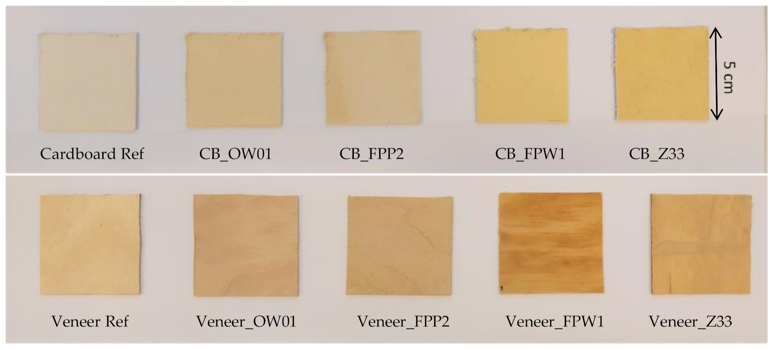
The substrate materials selected for this study were PankaMax cardboard (CB) from Pankaboard, Pankakoski, Finland (thickness of 1.75 mm and area density of 650 g/m2) and KoskiPly Birch Exterior AB/B (1.5 mm thick veneer) from Koskisen Oy, Kärkölä, Finland.
The fire-retardant materials selected for use were FireProof P2 and FireProof W1 from Kiilto Oy (Kiilto Oy, Lempäälä, Finland), Organowood® (Organowood AB, Täby, Sweden) Protection 01 from OrganoWood AB and Zeopol® 33 from Evonik (Evonik Resource Efficiency GmbH, Hanau-Wolfgang; Germany). FireProof P2 (FPP2) is an environmentally safe fire retardant designed for paper and cardboard applications. It is a liquid suitable for spray spreading with a density of 1.25 g/m3, a pH of 13, and dry material content of 27%. It should meet fire class E (SFS-EN ISO 11925) if applied at 10 g/m2 on cardboard. FireProof W1 (FPW1) is a fire retardant, which is specifically developed for treatment of spruce veneer, using spray or brush coating. It has a pH between 5–7 and a DIN 4 viscosity of 13 ± 2 s. It is specified to meet Euroclass B-s1 d0 when applied (on spruce veneer) at 250 g/m2. OrganoWood® Protection 01 (OW01) is a water-based wood treatment product composed of silicon minerals and natural plant compounds. It is intended for use in the surface treatment of wooden products, such as solid wood or particleboards. It is a transparent liquid with a density between 1.2–1.4 g/m3 and a pH of 10–11. When used for spruce panel coating, it meets reaction to fire classification Cs1 d0, according to EN13501-1 as dipped on surface at 0.33 L/m2 (about 250 g/m2). Zeopol® 33 (Z33) is a clear low viscous sodium silicate solution with 37% dry material content, a density of 1.378 g/m3 and pH of 11. It is suitable for spray spreading and is widely used in pulping or the recycled paper industry.
The ink used for the screen-printing trials was Asahi LS-411AW microparticle silver paste from Asahi Chemical Research Laboratory. It is a one-component, polymer-type silver paste with a polyester binder. It has a solid content of 75–78% and a viscosity of 200–300 ps at 25 °C. The ink is cured at 150 °C for 20 min. The typical sheet resistance for a 10 µm layer is <40 mΩ/sq.
2.2. Coating with Fire Retardants
Fire-retardant coatings were applied using the spray method on one side of the substrates. The application amounts are displayed in
Table 1. Of the fire-retardants used, OW01 was the easiest to apply, using a spray. Spraying was performed in a fume hood and drying was done in an oven with an exhaust exit to outside air. The application of Z33 using the spray method was quite similar to that of OW01, but first needed dilution from the original dry material content of 20% to 10% using purified water. The application of FPP2 required that some practical additional protection measures were taken in addition to the earlier protection measures of gloves, goggles, and fume hood. The fume hood was protected with a plastic film for easier cleaning, and a protective suit (Tyvek PRO-TECH F TOPGUARD) (Indutex GmbH, Krefeld, Germany) and gas mask (A2B2E2K2-P3 R filter) (3M, Cummins’ Neillsville, Wisconsin, USA) were also used. Any waste created were handled as hazardous waste. The same measures were followed for application of FPW1 as well, as it can corrode the metal of the fume hood.
2.3. Analytics for Surface Characteristics
A Theta optical tensiometer (Biolin Scientific, Gothenburg, Sweden) was used for measuring the contact angle of water on the uncoated and coated surfaces. Samples were conditioned and measured at 23 °C and 50% relative humidity. Measurements were performed with deionized water at a drop volume of 3 µL. The reported contact angle values are average values from five measurements.
The surface roughness of the uncoated and coated samples was measured from a 15 × 15 mm area using a Keyence VR-3200 optical 3D-profilometer (Keyence, Itasca, Illinois, USA). The reported roughness values are the roughness averages of the measured areas.
2.4. Limiting Oxygen Index (LOI)
The flame resistance of the fire-retardant-coated substrates was evaluated by the limiting oxygen index method (LOI), according to ISO 4589-2:2017. The standard specified methods for determining the minimum volume fraction of oxygen, in an admixture with nitrogen that will support combustion of small vertical test specimens under specified test conditions. The results are defined as oxygen index (OI) values. Samples were cut from coated cardboard or veneers into 2-cm-wide and 20-cm-long self-standing samples. The samples are placed vertically on the sample holder, and the oxygen content is adjusted. The measurement is made by increasing the relative oxygen amount in steps of 0.5% compared to the nitrogen, igniting the samples from the top, and analyzing if the material catches fire and how long it will burn, both time wise and length wise. The result is when the material can sustain burning for 3 min or the burning length is 5 cm in under 3 min time. Typically, 0.5% differences show differences in material burning properties. In very homogeneous samples, even a smaller step can show a big difference. The result is based on four to six measurements.
2.5. Screen Printing
The printing tests were performed using an EKRA E2 sheet-based screen printer and Asahi LS-411AW microparticle silver paste. A 325-24 (mesh count (LPI), wire diameter (µm)) screen mesh, squeegee hardness and angle of 65 ShA/45°, and printing speed of 40 mm/s were used. The printed samples were dried with hot air in a box oven at 150 °C for 20 min. The layout consisted of a conductor line and line space patterns with varying width (100, 150, 200, 300, 500, and 1000 µm) and orientation, as well as larger (1.5 × 1.5 cm) rectangular areas.
2.6. Analytics for Printed Patterns
The resistance (R) of printed samples with a size of 15 × 15 mm square was measured using a digital multimeter Keithley 2700 (Keithley Instruments LLC, Solon, Ohio, USA) connected to a four-point probe setup with probing tips arranged linearly with an equal 600 µm spacing. The equation for an infinite sheet, where the thickness of the layer is much smaller than the probe spacing, was then used for calculating the sheet resistance
For the line samples, the resistance (R) was measured using a digital multimeter (Keithley 2700). Using the width (w) and length (l) of the line, the following equation for calculating the sheet resistance (Rs) was applied:
An optical microscope was used to study the print quality attributes of the printed line space patterns. The number of measurements for the square patterns was ten and a maximum of five for the lines, due to a limited number of uniform printed lines in samples.
2.7. SEM
The morphology of samples was studied using a Scanning Electron Microscope (SEM) JEOL JSM T100 (JEOL Ltd., Tokyo, Japan) with a voltage of 10 kV. Images were taken from the cross-cut surface of samples containing a silver printed pattern.
2.8. Biodegradation in Soil
The biodegradability of materials was evaluated using ISO 17665:2012, which is based on CO2 evolution. Instead of passing carbon-dioxide-free air over the soil, and then determining the carbon dioxide content of the air as described in the standard, CO2 concentrations were analyzed from the head space volumes without passing air over soil.
Soil was collected from an agricultural field located in Helsinki, Finland. The pH of the soil was 6.4, organic matter content was 9% (dry weight) and the C/N ratio was 19. The soil was sieved to a 2 mm particle size, and the final soil moisture content was adjusted to 76% (~30% of the water holding capacity). For each replicate, 500 mg of material was mixed with 75 g of soil (dry weight) in a 1000 mL glass bottle sealed with septum and screw cap with a hole. Three replicates were prepared for each tested material, for blank and for microcrystalline cellulose with particle size 20 µm (Sigma-Aldrich/ Merck KGaA, Darmstadt, Germany) that was used as a reference compound. Samples were milled using an IKA A11 analytical mill (IKA, Staufen, Germany) and sieved to a 500 µm particle size. The carbon content of the materials and the nitrogen and carbon content of the soil were evaluated using a Flash 2000 EA CHNS-O (Thermo Fisher Scientific Oy, Espoo, Finland) elemental analyzer.
Carbon dioxide concentrations in the head space volumes of the bottles were measured at regular intervals by inserting a needle through the septum of the bottles and directly measuring the CO2 concentration using a Servoflex MiniFoodPack 5200 infrared analyzer (Servomex, Crowborough, UK). Bottles were aerated to remove excess CO2, closed with a septum and screw cap, and CO2 concentrations were measured for a second time. The net CO2 production from the test materials was calculated by subtracting the average amount of CO2 produced in the blank soils (no sample) from the amount of CO2 produced in the test material bottles. The biodegradation percentages were calculated from the ratio between the net CO2 production and the theoretical CO2 production calculated on the basis of the elemental carbon content of the material.
4. Discussion
The aim of this work was to analyze if there is any possibility for wood-based materials, such as cardboard or veneer, to act as substrate materials for printed electronics, focusing on printed circuit boards (PCB) manufactured by screen printing. Potential application areas for wood-based PCBs would be, for example, in environmental monitoring where biodegradability is needed. An extra-bulky, uncoated cardboard (CB) and 1.5 mm thick birch veneer were selected as base materials. To provide some level of fire resistance for the selected substrates, and to provide smoother surfaces for screen-printing, the substrates were coated with fire retardants.
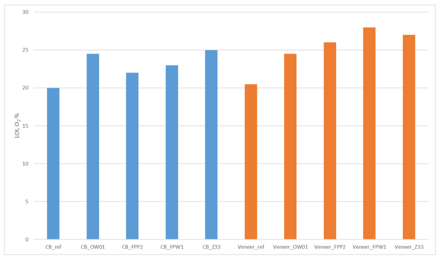
Four different fire-retardant (FR) materials were selected for testing and were spray coated on the substrates without adjusting the viscosity to the same level. OW01 and Z33 are silicon containing water-based materials, FPP2 is a commercial FR material designed for cardboard applications and FPW1 is a commercial FR material developed for spruce veneer. The application varied on CB from 17 to 143 g/m2. OW01 was applied at the lowest level, and it is specified to attain C classification when applied at 250 g/m2 using dip-coating. However, the 17 g/m2 amount, when absorbed on the cardboard fiber structure, was able to provide some protection as indicated by the LOI value of 24.5 O2-%. Z33 was absorbed onto the fiber structure at 37 g/m2 and gave the best fire resistance (LOI value of 25 O2-%). FPP2 should meet fire class E in the amount of 10 g/m2. Here it was applied at 44 g/m2 on the cardboard surface and provided a LOI value of 22 O2-%. Exceeding an LOI value of 21 O2-% indicates that the material requires a higher oxygen content to support combustion than is provided under normal conditions.
The applied FR amounts on veneer varied from 34 g/m2 (OW01) to 84 g/m2 (FPW1). The best fire protection was attained with FPW1 at an LOI value of 28 O2-%, which is a very good results as it is suggested to be used in the amounts of 250 g/m2 on veneer to meet the fire class C. Z33 was nearly as effective providing an LOI of 27 O2-% when applied at only 48 g/m2. It must be noted that LOI gives only an indication of material flammability resistance and does not confer any classification compliance. However, it does appear that Z33- or FPW1-coated veneer have the potential to provide some fire resistance for PCB solutions against electrical short circuits potentially causing ignition.
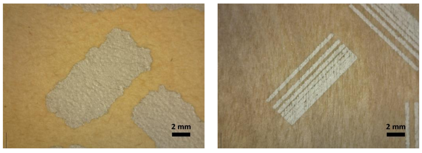
All the tested coatings gave higher roughness values and a lower contact angle, providing the surface with increased hydrophilicity for the carboard. The higher roughness and lower contact angle properties affected screen printing as wider line widths were observed compared to neat cardboard. The effects of these properties also resulted in higher sheet resistance values for the coated cardboards especially for 0.5 × 18 mm line pattern areas (see
Table 3). The sheet resistance over the 15 × 15 mm squares for the cardboard samples ranges from 36 to 51 mΩ/sq, which is close to the optimal sheet resistivity level given for the silver ink used in screen printing (<40 mΩ/sq for 10 µm line thickness). The thickness of printed patterns is in the level of 20 to 50 µm and presented in
Figure 5.
Figure 3 and
Figure 4 show that the lines are spread on the cardboard surface with no visible gap between them when printed close to each other. The roughness of the uncoated veneer was 6.6 µm being clearly smoother than that of the uncoated cardboard (22.6 µm).
The application of the OW01 and FPW1 FR coatings resulted in smoother surfaces that that of the untreated veneer as indicated by the roughness values of 6.0 µm and 1.2 µm, respectively. The roughness of coated veneer was 7.4 µm with Z33 and 10.2 µm with FPP2. The contact angle of veneer dropped significantly (from 103°) with all the FR coatings indicating a higher levelling of water and probably an improved levelling of printing inks on the surface. The characteristic of the veneer surface changed from hydrophobic when uncoated (>90°) to hydrophilic (<90°) after coating. The same change of hydrophobicity was also found for coated and uncoated cardboard. The line quality for the veneer samples was good, showing line widths of 400 (OW1) to 458 µm (uncoated) for a nominal screen-printed line width of 500 µm (see
Table 3). The minimum gap width was smallest (150 µm) on the uncoated veneer which also featured the highest contact angle.
For the uncoated veneer, the sheet resistance over the 0.5 × 8 mm line pattern areas were unmeasurable due to line breaks and was 91 mΩ/sq over the 15 × 15 mm square areas. The best overall performance of the coated veneer samples was found with Z33 which provided sheet resistance of 71 mΩ/sq over the line pattern areas and 100 mΩ/sq over the square areas and also provided the best visual appearance for the printed patterns. A sheet resistance range of 300–600 mΩ for Al-coated veneer was reported by Wang et al. [
20]. Li et al. coated veneer by sputtering copper on the surface at different temperatures and observed increases in sheet resistance from 40 mΩ up to >300 mΩ when the application temperature was raised from room temperature to 200 °C. It was assumed that, at higher temperatures, these increases may be caused by a reduction of the copper layer, due to a diffusion of ink on the surface or increases of surface roughness at an elevated temperature from the destruction of sealing strata on wood veneer [
21]. The silver ink curing used in the work reported here was 20 min at 150 °C, and it is possible that similar effects on the veneer, which probably contains lignin and hemicellulose, may occur under the FR-coating. Unfortunately, surface properties were not analyzed after printing, but could be done in further studies. A similar increase in sheet resistance was not found for the FR-coated dense cardboard over the square areas.
If printed electronics are used in applications which end up in a natural environment, biodegradability is a desired property. Potential applications include, for example, sensors for precision agriculture when used in multitude, and collection after use is not feasible, and sensors for monitoring environmental conditions, such as weather with remote connection. Biodegradability is also important when considering the concept of single-use electronics, such as disposable health monitoring test devices, e.g., digital pregnancy tests ending up in domestic waste. Another example is electronic devices attached to compostable products, such as cellulose-based packages. In all of these cases, the electronics end up in a biological environment after use or is not collected properly for recycling, and creation of a new source of electronic waste should be avoided.
In this study, biodegradation of uncoated veneer and cardboard, used as a substrate material, was evaluated in a soil environment. Compared to a microcrystalline cellulose reference compound, the relative biodegradability of veneer and cardboard in the soil was 52% and 33%, respectively. There are no requirements available for the biodegradability of printed electronics in soil, but ISO 17,665 sets requirements for biodegradable mulching films used in agriculture. According to the standard, the relative biodegradation should be 90% of reference material in order to be considered as biodegradable.
One explanation for the low biodegradability values is that both veneer and cardboard contain considerable amounts of lignin. PankaMax cardboard is manufactured from groundwood pulp typically containing 27% of lignin. Veneer is composed of thin slices of wood bound together by glue. Lignin is known to reduce the biodegradability of cellulosic materials relative to complete mineralization and CO
2 evolution [
22,
23]. It has also been demonstrated that a substantial fraction of
14C-labelled synthetic lignin was incorporated into humic compounds or other insolubles during composting, and only a minor part of the lignin was mineralized to carbon dioxide [
24]. Similar behavior was observed in soil as disintegration of paper mulches in agricultural soil was reduced with increasing lignin content [
25]. The formation of lignin is beneficial for soil but is difficult to take into consideration when the biodegradability of lignin-containing samples is evaluated.
In addition to lignin, other compounds and additives in veneer and cardboard can influence their biodegradability. The detailed composition of studied materials is not known, but a typical binder used in veneer is phenol formaldehyde, which has limited biodegradability [
26]. When materials for PCB substrates are selected, the biodegradability of all material components, including coatings, as well as their environmental safety, should be considered.
Biodegradability is a complex topic, and merely employing biodegradable substrates is not sufficient for producing biodegradable electronics. There are numerous other printed and assembled components and circuitry required for achieving sufficient electrical performance, and biodegradability of these aspects should be studied in the future.


 ,
, 


