
A Numerical Analysis of Ductile Deformation during Nanocutting of Silicon Carbide via Molecular Dynamics Simulation


Abstract
:1. Introduction
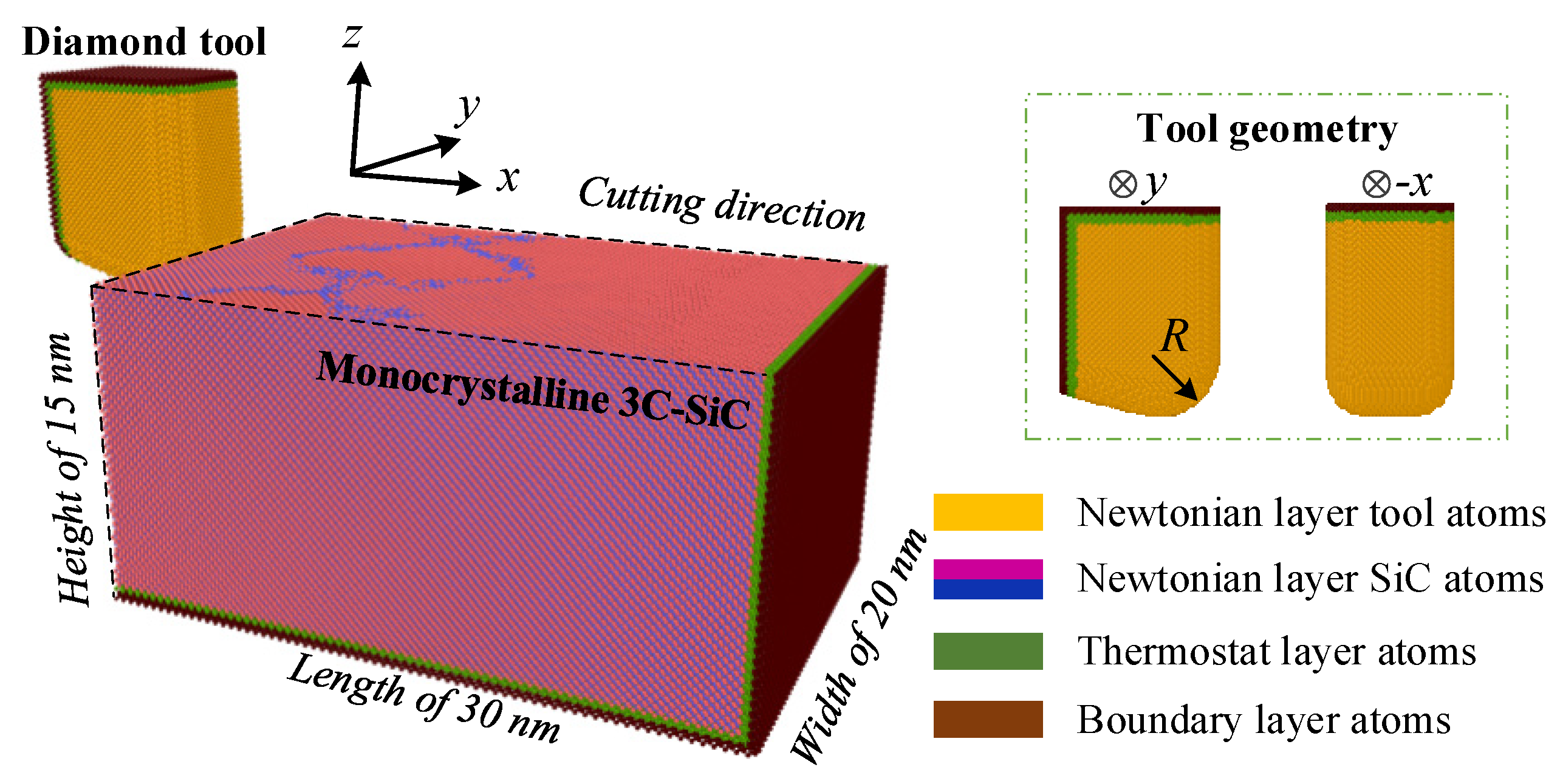
2. Modelling
3. Results and Discussion
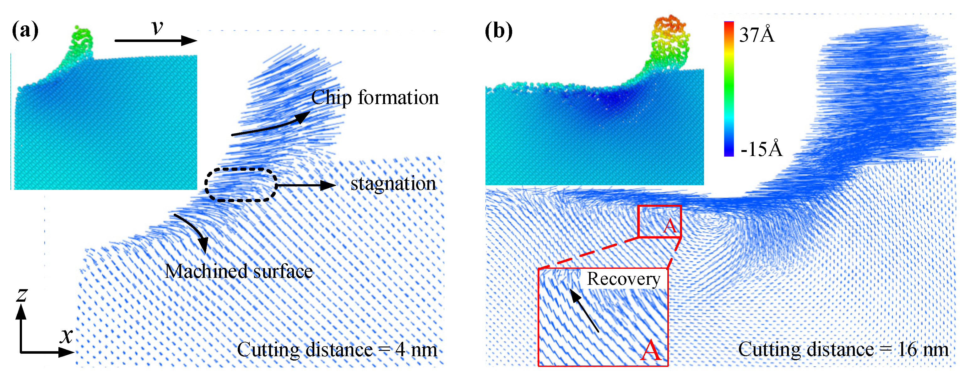
3.1. Ductile Machining Mechanism
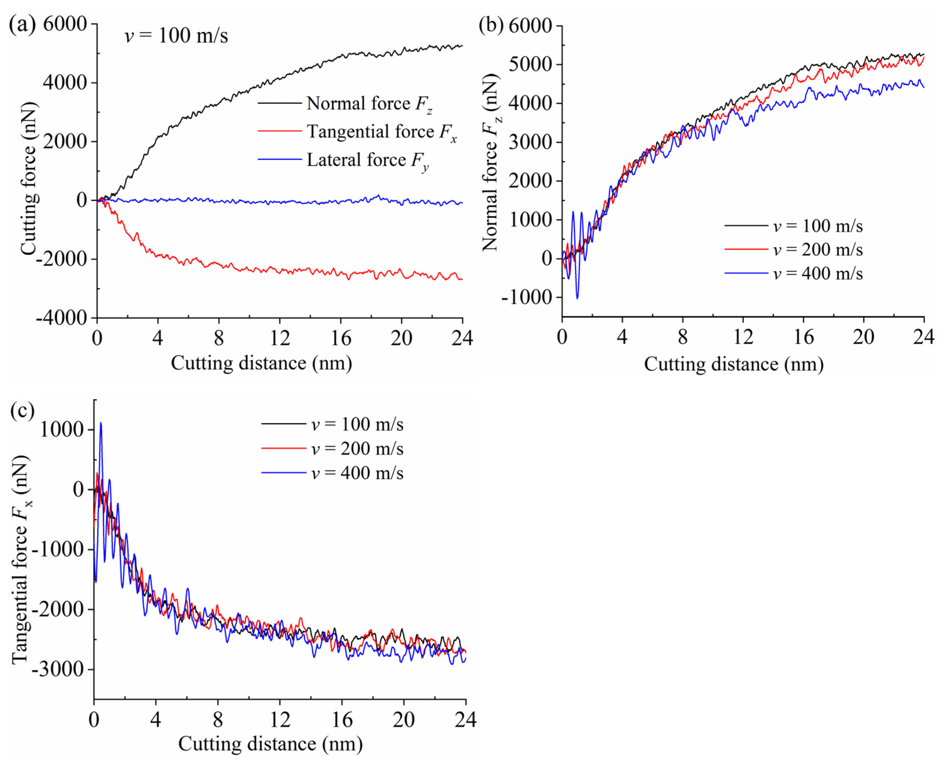
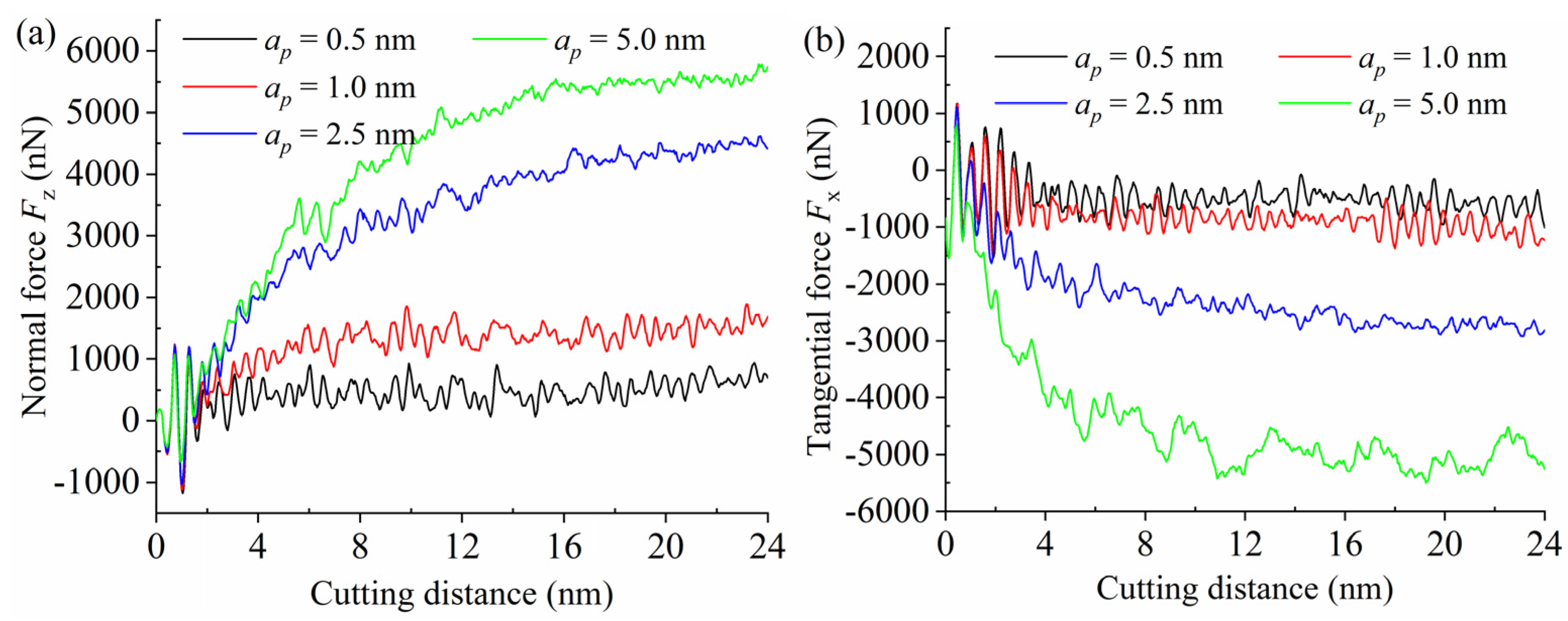
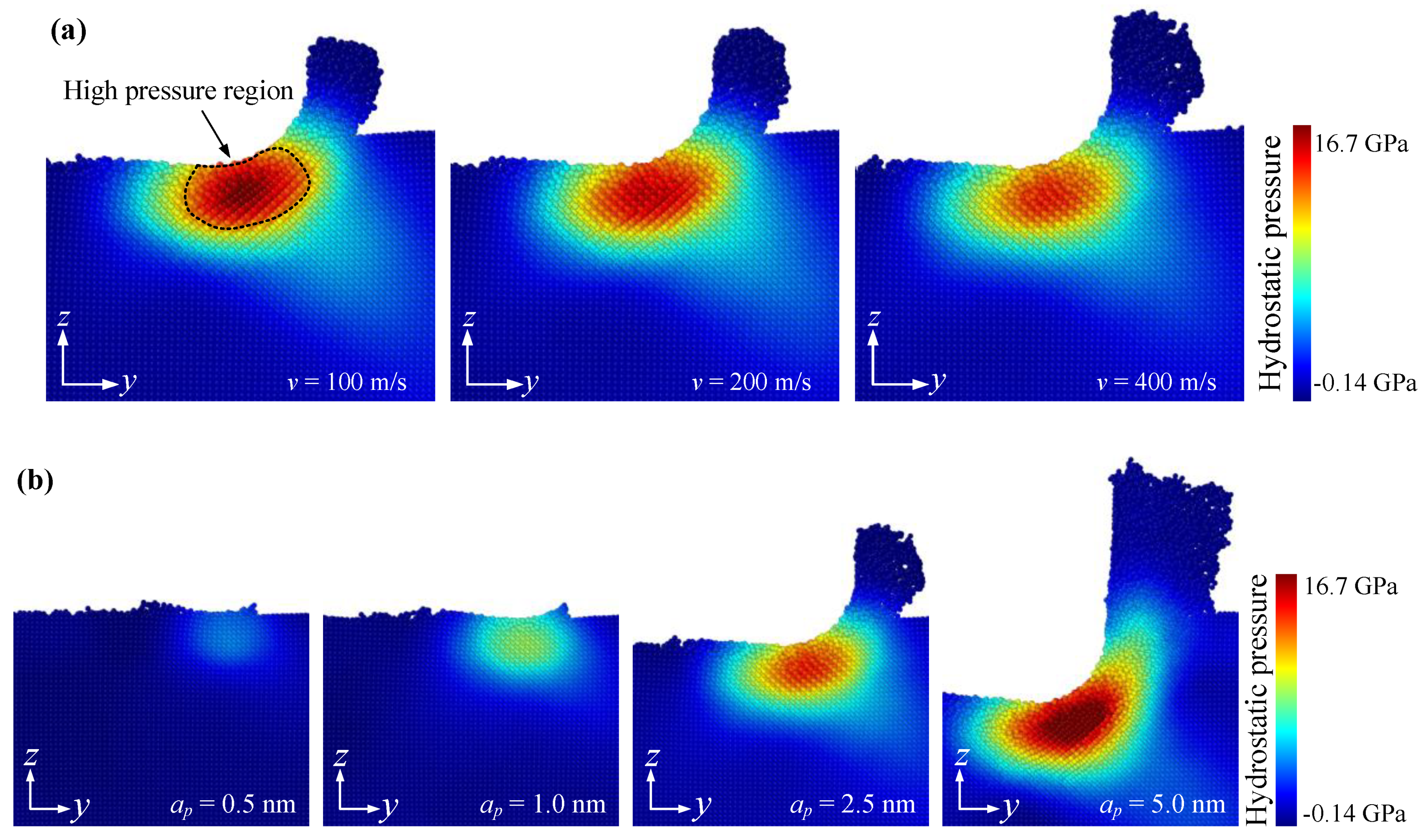
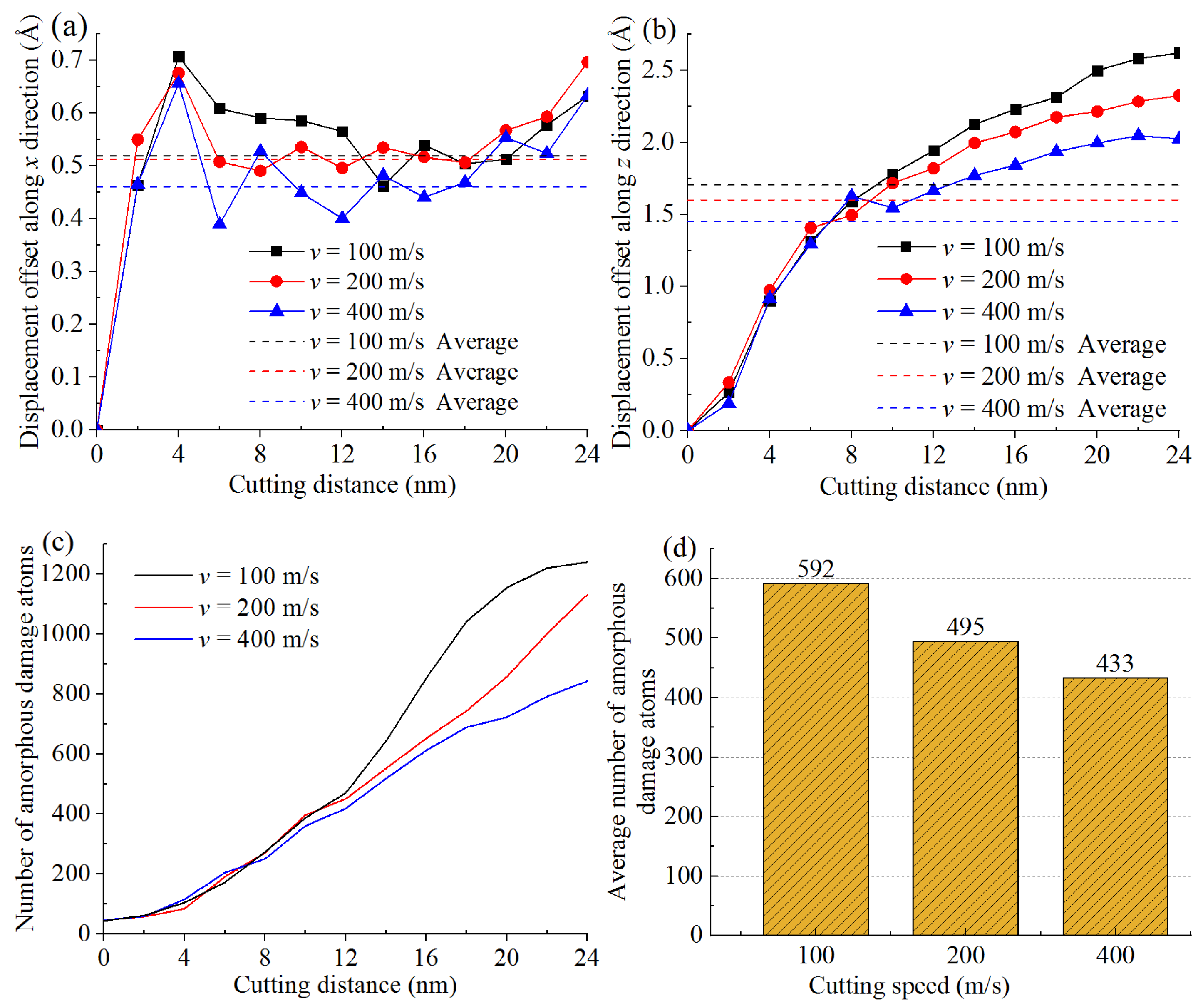
3.2. Cutting Force and Hydrostatic Pressure
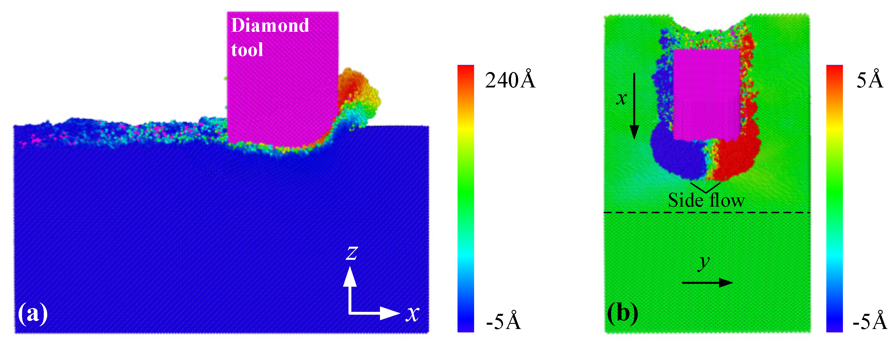
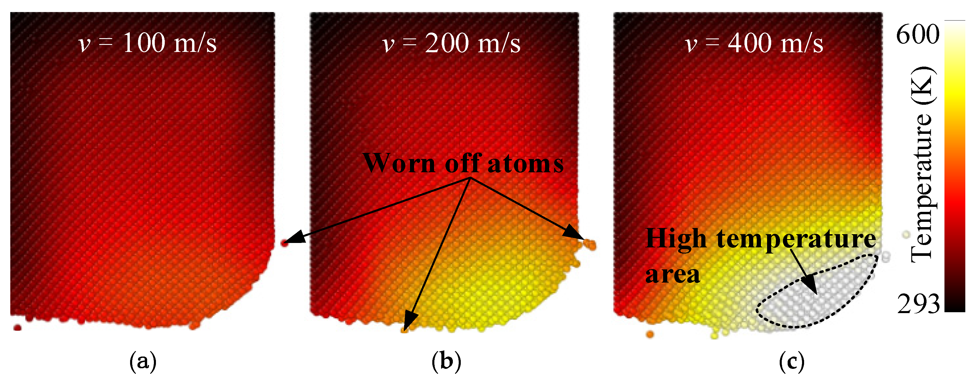
3.3. Tool Wear
4. Conclusions
- (1)
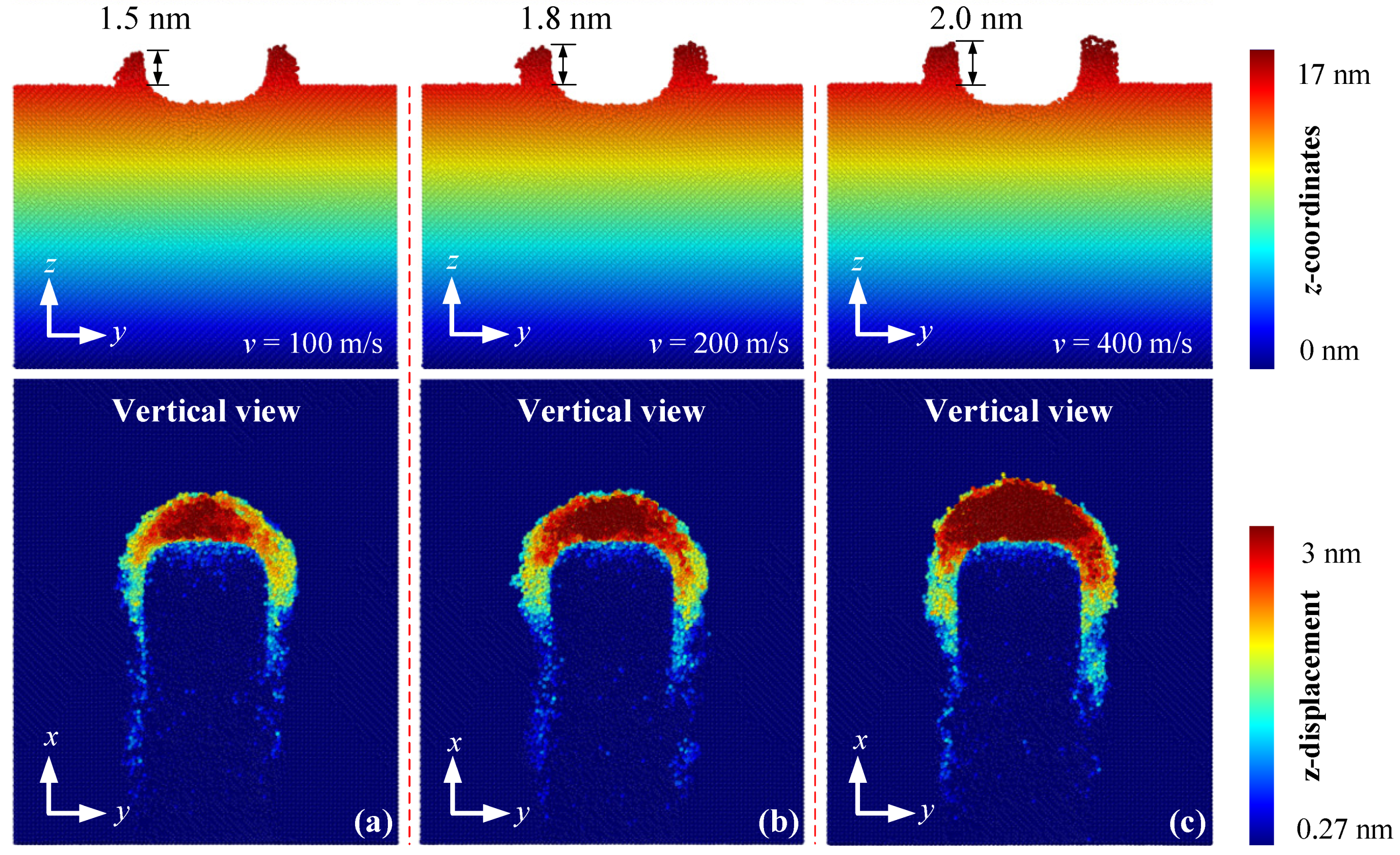
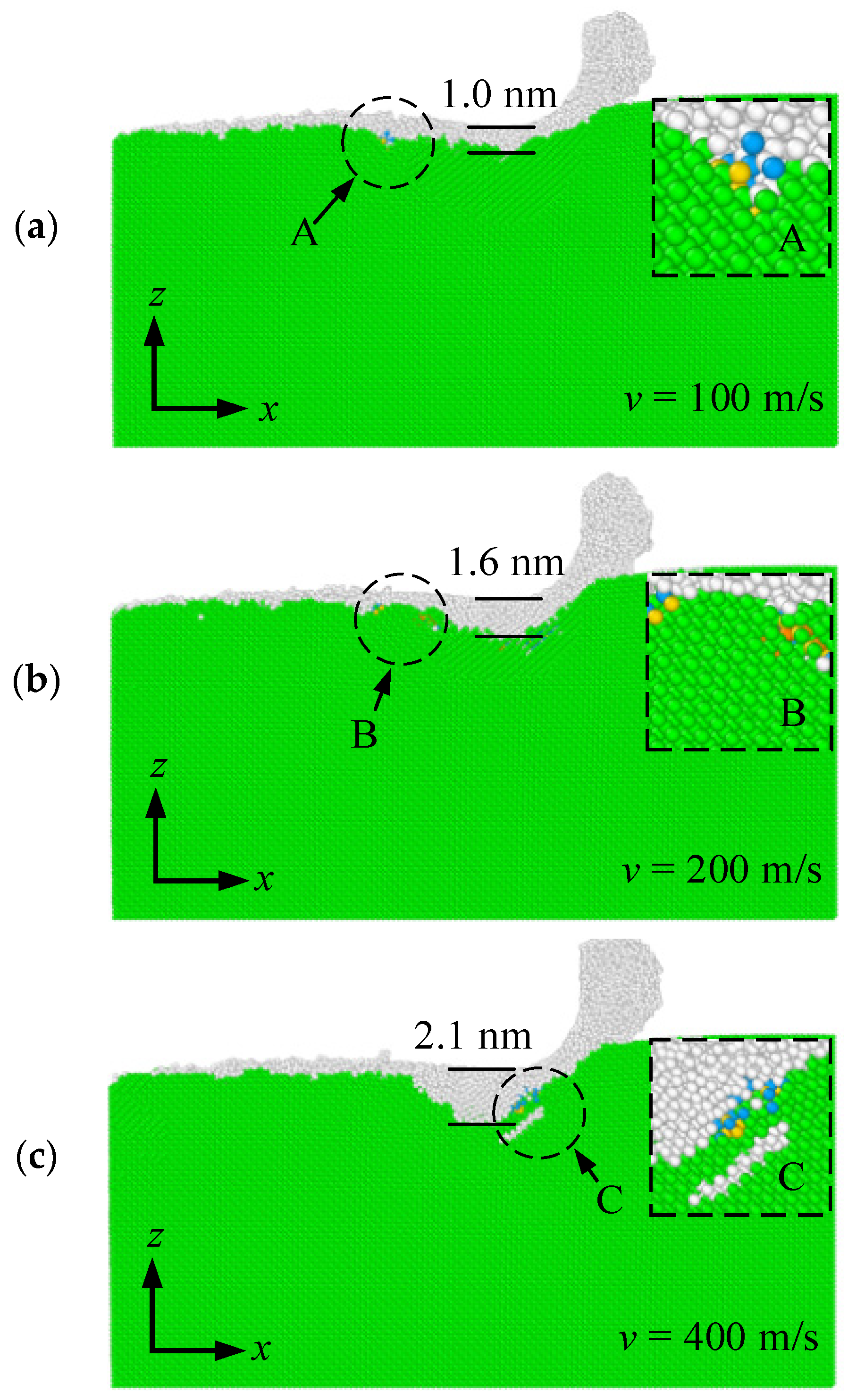
- Nanometric cutting at a higher speed was able to effectively improve the material removal rate, and reduce the cutting force and hydrostatic pressure, which were the favorable impacts. At the same time, it brought some adverse impacts, such as reducing the quality of machined surface and increasing the thickness of subsurface damage layer.
- (2)
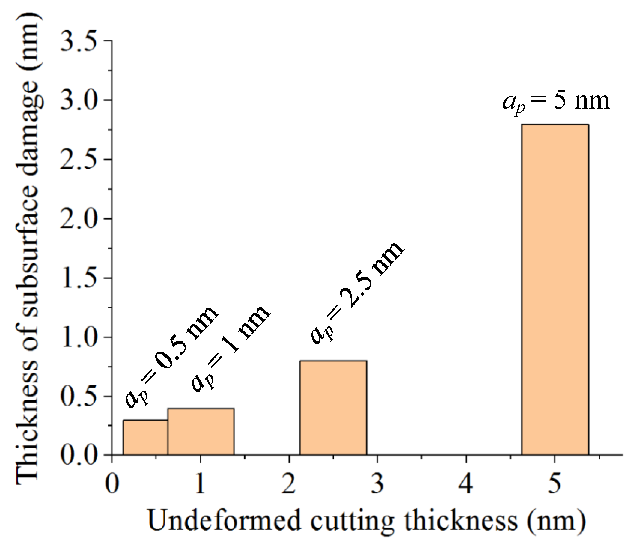
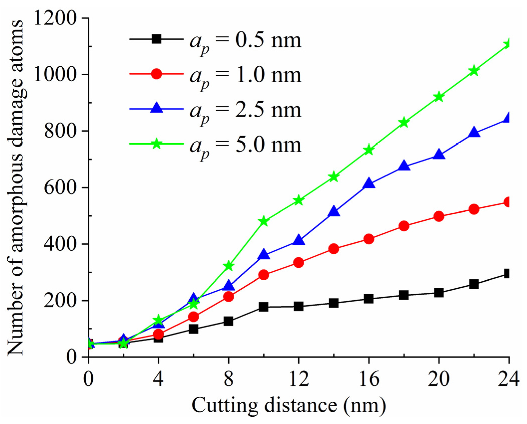
- In the nanometric cutting, the chip formation was dominated by the extrusion action rather than the shear theory. Nanometric cutting with a larger undeformed cutting thickness can improve the processing efficiency, however, it would enlarge the thickness of the subsurface damage layer, produce much more dislocation atoms, and increase the hydrostatic pressure.
- (3)
- The maximum temperature of the tool was concentrated at the transition arc between the tool rake face and clearance face, which was obviously distinct from that in the nanometric cutting of ductile material. The performance and service life of the diamond tool can be effectively improved by properly increasing the cutting speed and reducing the undeformed cutting thickness.
Author Contributions
Funding
Institutional Review Board Statement
Informed Consent Statement
Data Availability Statement
Acknowledgments
Conflicts of Interest
References
- Kalkhoran, S.N.A.; Vahdati, M.; Yan, J. Effect of relative tool sharpness on subsurface damage and material recovery in nanometric cutting of mono-crystalline silicon: A molecular dynamics approach. Mater. Sci. Semicond. Process. 2020, 108, 104868. [Google Scholar] [CrossRef]
- Liu, C.; Chen, X.; Ke, J.; She, Z.; Xu, J. Numerical investigation on subsurface damage in nanometric cutting of single-crystal silicon at elevated temperatures. J. Manuf. Process. 2021, 68, 1060–1071. [Google Scholar] [CrossRef]
- Liu, B.; Xu, Z.W.; Chen, C.; Pang, K.; Wang, Y.; Ruan, Q.H. Effect of tool edge radius on material removal mechanism of single-crystal silicon: Numerical and experimental study. Comput. Mater. Sci. 2019, 163, 127–133. [Google Scholar] [CrossRef]
- Liu, B.; Xu, Z.W.; Wang, Y.; Gao, X.; Kong, R.J. Effect of ion implantation on material removal mechanism of 6H-SiC in nano-cutting: A molecular dynamics study. Comput. Mater. Sci. 2020, 174, 109476. [Google Scholar] [CrossRef]
- Goel, S.; Luo, X.; Comley, P.; Reuben, R.L.; Cox, A. Brittle-ductile transition during diamond turning of single crystal silicon carbide. Int. J. Mach. Tool. Manuf. 2013, 65, 15–21. [Google Scholar] [CrossRef] [Green Version]
- Chavoshi, S.Z.; Luo, X.C. An atomistic simulation investigation on chip related phenomena in nanometric cutting of single crystal silicon at elevated temperatures. Comput. Mater. Sci. 2016, 113, 1–10. [Google Scholar] [CrossRef] [Green Version]
- Zhang, K.; Liu, G.Z.; Gao, H.Y.; Sun, H.; Tang, Y.L.; Tang, Y.L.; Wu, Y.H. Effect of machining parameters on Nnano-cutting of SiC ceramics. Adv. Mater. Res. 2012, 472–475, 1069–1073. [Google Scholar] [CrossRef]
- Ding, K.; Fu, Y.C.; Su, H.H.; Xu, H.X.; Cui, F.F.; Li, Q.L. Experimental studies on matching performance of grinding and vibration parameters in ultrasonic assisted grinding of SiC ceramics. Int. J. Adv. Manuf. Tech. 2017, 88, 2527–2535. [Google Scholar] [CrossRef]
- Pan, J.S.; Yan, Q.S.; Li, W.H.; Zhang, X.W. A nanomechanical analysis of deformation characteristics of 6H-SiC using an indenter and abrasives in different fixed methods. Micromachines 2019, 10, 332. [Google Scholar] [CrossRef] [Green Version]
- Prasad, K.E.; Ramesh, K.T. Hardness and mechanical anisotropy of hexagonal SiC single crystal polytypes. J. Alloy. Compd. 2019, 770, 158–165. [Google Scholar] [CrossRef]
- Shimada, S.; Ikawa, N.; Inamura, T.; Takezawa, N.; Ohmori, H.; Sata, T. Brittle-Ductile transition phenomena in microindentation and micromachining. CIRP Ann. Manuf. Tech. 1995, 44, 523–526. [Google Scholar] [CrossRef]
- Liu, Y.; Li, B.Z.; Kong, L.F. Molecular dynamics simulation of silicon carbide nanoscale material removal behavior. Ceram. Int. 2018, 44, 11910–11913. [Google Scholar] [CrossRef]
- Meng, B.; Yuan, D.; Zheng, J.; Xu, S. Molecular dynamics study on femtosecond laser aided machining of monocrystalline silicon carbide. Mat. Sci. Semicon. Proc. 2019, 101, 1–9. [Google Scholar] [CrossRef]
- Zhao, L.; Hu, W.J.; Zhang, Q.; Zhang, J.J.; Zhang, J.G.; Sun, T. Atomistic origin of brittle-to-ductile transition behavior of polycrystalline 3C-SiC in diamond cutting. Ceram. Int. 2021, 47, 23895–23904. [Google Scholar] [CrossRef]
- Zhang, J.J.; Han, L.; Zhang, J.G.; Liu, H.Y.; Yan, Y.D.; Sun, T. Brittle-to-ductile transition in elliptical vibration-assisted diamond cutting of reaction-bonded silicon carbide. J. Manuf. Proc. 2019, 45, 670–681. [Google Scholar] [CrossRef]
- Xiao, G.B.; Ren, M.J.; To, S. A study of mechanics in brittle-ductile cutting mode transition. Micromachines 2018, 9, 49. [Google Scholar] [CrossRef] [Green Version]
- Liu, H.T.; Xie, W.K.; Sun, Y.Z.; Zhu, X.F.; Wang, M.H. Investigations on brittle-ductile cutting transition and crack formation in diamond cutting of mono-crystalline silicon. Int. J. Adv. Manuf. Tech. 2018, 95, 317–326. [Google Scholar] [CrossRef]
- Peng, T.; Xu, X. Energy-efficient machining systems: A critical review. Int. J. Adv. Manuf. Tech. 2014, 72, 1389–1406. [Google Scholar] [CrossRef]
- Tan, T.H.; Yan, J.W. Atomic-scale characterization of subsurface damage and structural changes of single-crystal silicon carbide subjected to electrical discharge machining. Acta Mater. 2017, 123, 362–372. [Google Scholar] [CrossRef]
- Basa, A.; Wang, D.; Espallargas, N.; Wan, D. An in-situ electrochemical nanoindentation (ECNI) study on the effect of hydrogen on the mechanical properties of 316L austenitic stainless steel. Materials 2021, 14, 6426. [Google Scholar] [CrossRef]
- Shibata, T.; Ono, A.; Kurihara, K.; Makino, E.; Ikeda, M. Cross-section transmission electron microscope observations of diamond-turned single-crystal Si surfaces. Appl. Phys. Lett. 1994, 65, 2553–2555. [Google Scholar] [CrossRef]
- Ji, C.H.; Shi, J.; Liu, Z.Q.; Wang, Y.C. Comparison of tool-chip stress distributions in nano-machining of monocrystalline silicon and copper. Int. J. Mech. Sci. 2013, 77, 30–39. [Google Scholar] [CrossRef]
- Chavoshi, S.Z.; Luo, X.C. Molecular dynamics simulation study of deformation mechanisms in 3C-SiC during nanometric cutting at elevated temperatures. Mat. Sci. Eng. A 2016, 654, 400–417. [Google Scholar] [CrossRef] [Green Version]
- Stukowski, A. Visualization and analysis of atomistic simulation data with OVITO-the Open Visualization Tool. Modell. Simul. Mater. Sci. Eng. 2010, 18, 2154–2162. [Google Scholar] [CrossRef]
- Zhu, P.Z.; Qiu, C.; Fang, F.Z.; Yuan, D.D.; Shen, X.C. Molecular dynamics simulations of nanometric cutting mechanisms of amorphous alloy. Appl. Surf. Sci. 2014, 317, 432–442. [Google Scholar] [CrossRef]
- Guo, Y.B.; Liang, Y.C. Atomistic simulation of thermal effects and defect structures during nanomachining of copper. Trans. Nonferr. Metal. Soc. 2012, 22, 2762–2770. [Google Scholar] [CrossRef]
- Bohdal, L.; Kulakowska, A.; Kulakowski, M. Finite element analysis and experimental investigation of cut surface formation of magnetic silicon steel in shear cutting. Materials 2021, 14, 6415. [Google Scholar] [CrossRef]
- Uysal, A.; Jawahir, I.S. A slip-line model for serrated chip formation in machining of stainless steel and validation. Int. J. Adv. Manuf. Tech. 2019, 101, 2449–2464. [Google Scholar] [CrossRef]
- Ajayi, O.O.; Abiola, A.; Ogbonnaya, M.; Michael, A. Development of thermomechanical model for the analysis of effects of friction and cutting speed on temperature distribution around AISI 316L during orthogonal machining. Procedia Manuf. 2016, 7, 682–687. [Google Scholar] [CrossRef]
- Tanaka, H.; Shimada, S. Guideline for ultra-precision machining of silicon carbide based on molecular dynamics analysis. In Proceedings of the 11th Euspen International Conference, Como, Italy, 23–26 May 2011. [Google Scholar] [CrossRef]


| Contents | Detailed Parameters |
|---|---|
| Workpiece | Material: Monocrystalline 3C-SiC |
| Dimensions: 30 × 20 × 15 nm3 | |
| Tool | Material: Nonrigid diamond |
| Rake angle: 0° | |
| Clearance angle: 15° | |
| Edge radius: 2.5 nm | |
| Cutting speed | 100, 200, 400 m/s |
| Undeformed cutting thickness | 0.5, 1.0, 2.5, 5.0 nm |
| Machining distance | 0–24 nm |
| Nanocutting direction | <1 −2 1 0> orientation on (0 0 0 1) plane |
| Initial temperature | 300 K |
| Thermostat method | NVT ensemble |
| Timestep | 1.0 fs |
| Potential function | ABOP Tersoff potential |
| Integration algorithm | Velocity-Verlet |
Publisher’s Note: MDPI stays neutral with regard to jurisdictional claims in published maps and institutional affiliations. |
© 2022 by the authors. Licensee MDPI, Basel, Switzerland. This article is an open access article distributed under the terms and conditions of the Creative Commons Attribution (CC BY) license (https://creativecommons.org/licenses/by/4.0/).
Share and Cite
Liu, B.; Li, X.; Kong, R.; Yang, H.; Jiang, L. A Numerical Analysis of Ductile Deformation during Nanocutting of Silicon Carbide via Molecular Dynamics Simulation. Materials 2022, 15, 2325. https://doi.org/10.3390/ma15062325
Liu B, Li X, Kong R, Yang H, Jiang L. A Numerical Analysis of Ductile Deformation during Nanocutting of Silicon Carbide via Molecular Dynamics Simulation. Materials. 2022; 15(6):2325. https://doi.org/10.3390/ma15062325
Chicago/Turabian StyleLiu, Bing, Xiaolin Li, Ruijie Kong, Haijie Yang, and Lili Jiang. 2022. "A Numerical Analysis of Ductile Deformation during Nanocutting of Silicon Carbide via Molecular Dynamics Simulation" Materials 15, no. 6: 2325. https://doi.org/10.3390/ma15062325
APA StyleLiu, B., Li, X., Kong, R., Yang, H., & Jiang, L. (2022). A Numerical Analysis of Ductile Deformation during Nanocutting of Silicon Carbide via Molecular Dynamics Simulation. Materials, 15(6), 2325. https://doi.org/10.3390/ma15062325