1. Introduction
In the Internet-of-things (IoT) era, energy-efficient and data processing speeds become the bottlenecks for further progress in informative operation technologies. High-density memories with the analog switching type are the basic need for neuromorphic computing [
1,
2]. Various analog-programmable emerging nonvolatile memory devices and, first of all, resistive random-access memories (RRAM), are cutting-edge technologies [
3,
4]. Because of the simple two-terminal design, a low-cost, cost-efficient, ultrahigh density, high-speed operating, etc., RRAM has become the most prospective candidate for emerging nonvolatile memory devices [
5,
6,
7,
8].
RRAM, also known as memristor, is an electronic device based on a metal-insulator-metal (MIM) structure, in which the internal resistance state is the recorded history of the applied voltage (or current), and the switching is the change of the state from a high-resistance state to a low-resistance state and back. The extremal parameters of RRAM are known for HfO
2 (extremely small device sized ~2 nm and only the minimal energy with a 6-bit/cell storage capacity) [
9,
10], and high-speed resistive switching (~few nanoseconds) is obtained for memristors based on AlN films [
11].
As the RRAM memristor size is scaled down to nanometer ranges, controlling the size and shape of the nanostructure electrode is very critical as RRAM defects can play an important role as a way to improve the electric field localization, increase the charge trapping ability, and also it can serve different purposes based on the structure design [
2].
A stable bipolar resistive switching effect with the ON/OFF current ratio amounting from one to 4–5 orders of magnitude is found for two-layer films of partially fluorinated graphene with graphene quantum dots (GQDs) and polyvinyl alcohol [
12]. Resistance switches were observed when the fluorination degree was relatively low (F/C ~20–25%), and quantum dots of graphene are the basis for the FG film conductivity. These structures are perspectives for nonvolatile memory cells, for the information storage, and data processing of flexible and printed electronics. The main problem of these structures is the size and quality of GQDs in the FG layer. GQDs are formed during the fluorination process in the hydrofluoric acid solution [
13,
14,
15]. To stop fluorination at a particular stage and create partially fluorinated material with required GQDs is a complicated task due to the strong fluorinated process dependence on a lot of graphene parameters (structural, morphological, and electrical).
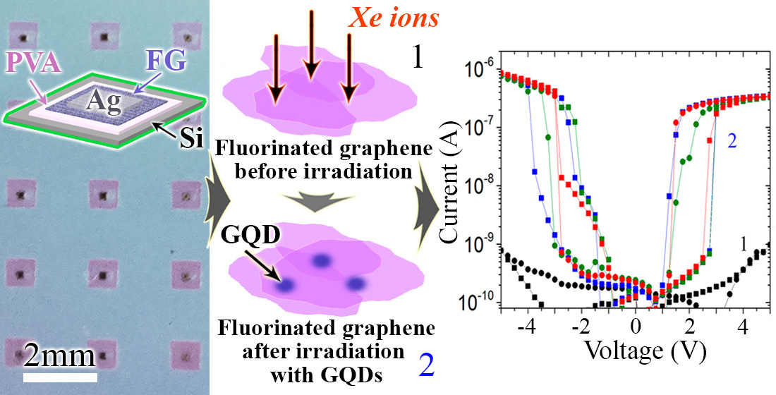
The new approach for creating GQDs in the fluorinated matrix, which is necessary for the memristive switchings, is suggested with the use of irradiation by heavy high-energy ions. According to our results, irradiation leads to the FG defluorination in the ion track area with the formation of 3–5 nm GQDs [
16]. In the present study, Xe ion irradiation was used to create the GQDs in 2D printed crossbar structures with an active dielectric FG film layer on PVA. As a result, the memristive effect with the ON/OFF current relation of ~2–4 orders of magnitude was observed in all irradiated structures, and the opening time was 30–40 ns. Thus, this approach is promising for the formation of two-phase memristor materials.
2. Materials and Methods
2.1. FG Suspension Preparation
The first stage of sample preparation is the fabrication of graphene suspensions. In this study, liquid exfoliation of natural graphite in combination with ultrasonic treatment and centrifugation was used. The fluorination process proceeds in a weak (~3–7%) aqueous hydrofluoric acid solution [
13,
14,
15]. In the process of fluorination, additional exfoliation greatly reduces the thickness of fluorinated graphene flakes to several monolayers. Simultaneously, the films obtained from the suspensions become smoother and more uniform [
13]. As a result, we created the FG suspension with a fluorination degree of F/C ~30–35%. This fluorination degree is the maximum of our fluorination approach and allows us to create dielectric films.
2.2. Fabrication of Memristor Structures
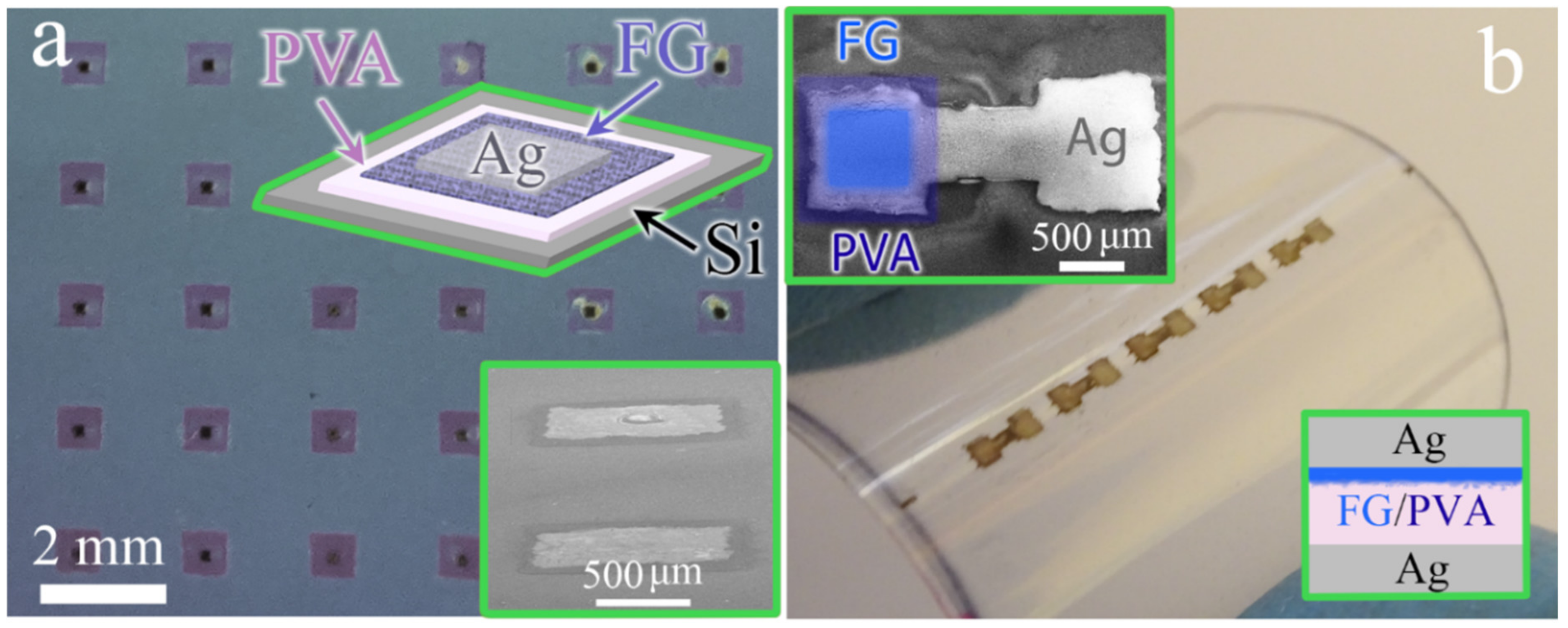
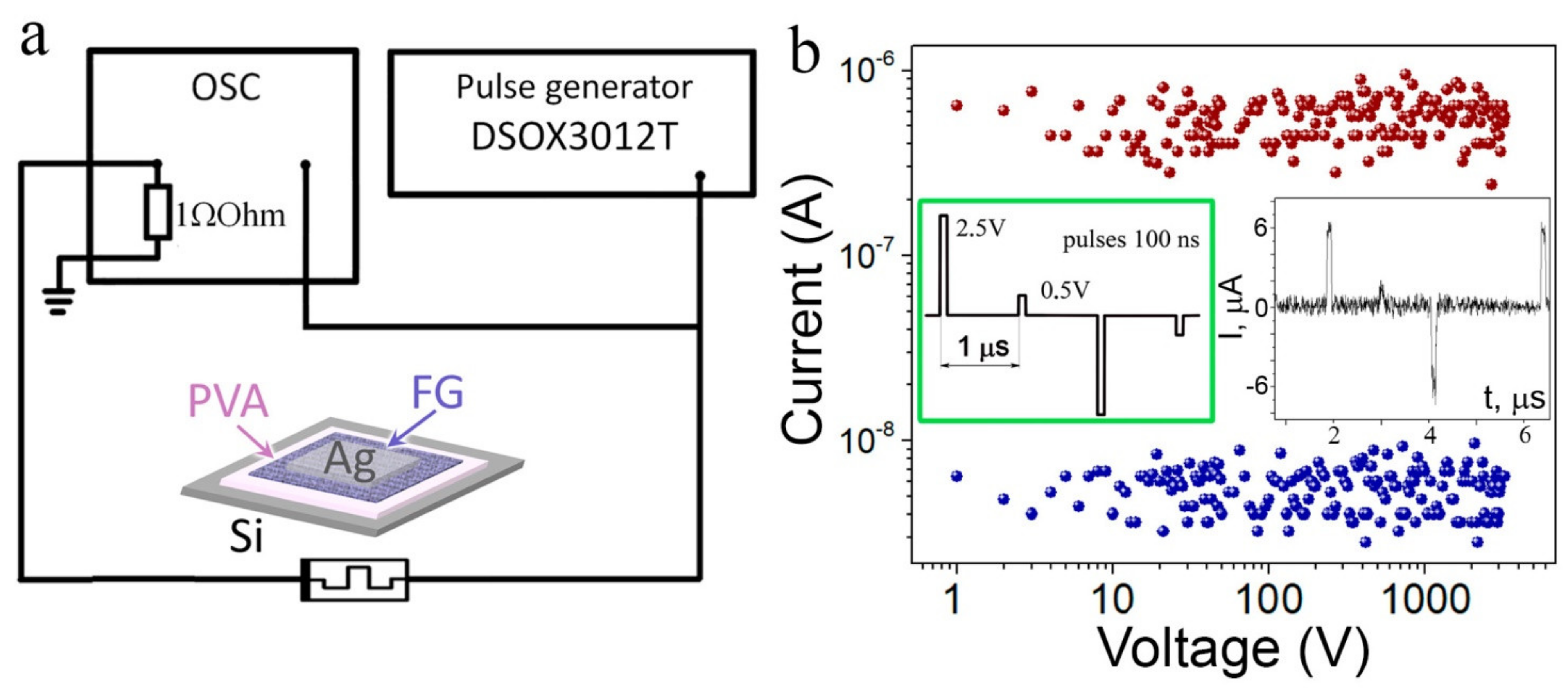
PVA was deposited on a silicon substrate or PET (polyethylene terephthalate) using a spin processor, and the deposited PVA layer thickness was 30 nm. In the present study, we have used PVA with a low molecular weight of 13,000–23,000 (Sigma-Aldrich, St. Louis, MI, USA). Fluorinated graphene has a fluorinated degree ~30–35%. The thickness of printed FG layers on PVA was varied from 4 nm to 20 nm with the step of 4 nm (5, 10, 15, 20, and 25 printed layers). The SEM and optical image of FG–PVA film, the schematic image of crossbar memristor structures, and the array of memristors printed on PET are presented in
Figure 1. The active memristor layer size in the structures is 900 × 900 μm
2. Ag inks were used for the bottom and top contacts with the line width of 300 × 300 μm
2 and the thickness of 200 nm. The upper Ag electrode for the crossbar structures was created after the ion irradiation of the active layers. The Ag contacts sheet resistivity was ~20 Ohm/sq. In some cases, silicon substrates were used as bottom contacts.
The polyvinyl alcohol used in the present study is short chains, and for this reason, PVA is a dielectric material. Fluorinated graphene before irradiation is also a dielectric material. The current-voltage characteristics for structures with an active layer created from PVA only or structures with FG layer are given in the
Supplementary Figure S1a,b.
2.3. Ion Irradiation Regimes
Irradiation was carried out by the Xe ions with the energy of either 26 MeV or 167 MeV; the fluences were 3 × 10¹⁰ and 3 × 1011 cm−2. The ion flux in the ion beam was 5.7 × 10⁸ ions/cm2s1 at room temperature, in a vacuum at the pressure of 6.3 × 10⁻⁶ Torr. The ion projected range (the ion penetration depth into the Si substrates) was equal to ~5 and ~19 μm for 26 and 167 MeV, respectively. Thus, the main part of defects introduced by ions are located in the substrates, and, in the thin active layer (35–50 nm, which consist of 30 nm of PVA and 5–20 nm of FG) of memristor structures, ion losses were connected with the ion interaction with the electron subsystem of the structures and atom ionization (electron losses). The ion irradiations were carried out on an ion-beam line for the applied research on the IC-100 cyclotron at FLNR JINR, Dubna.
2.4. Experimental Techniques
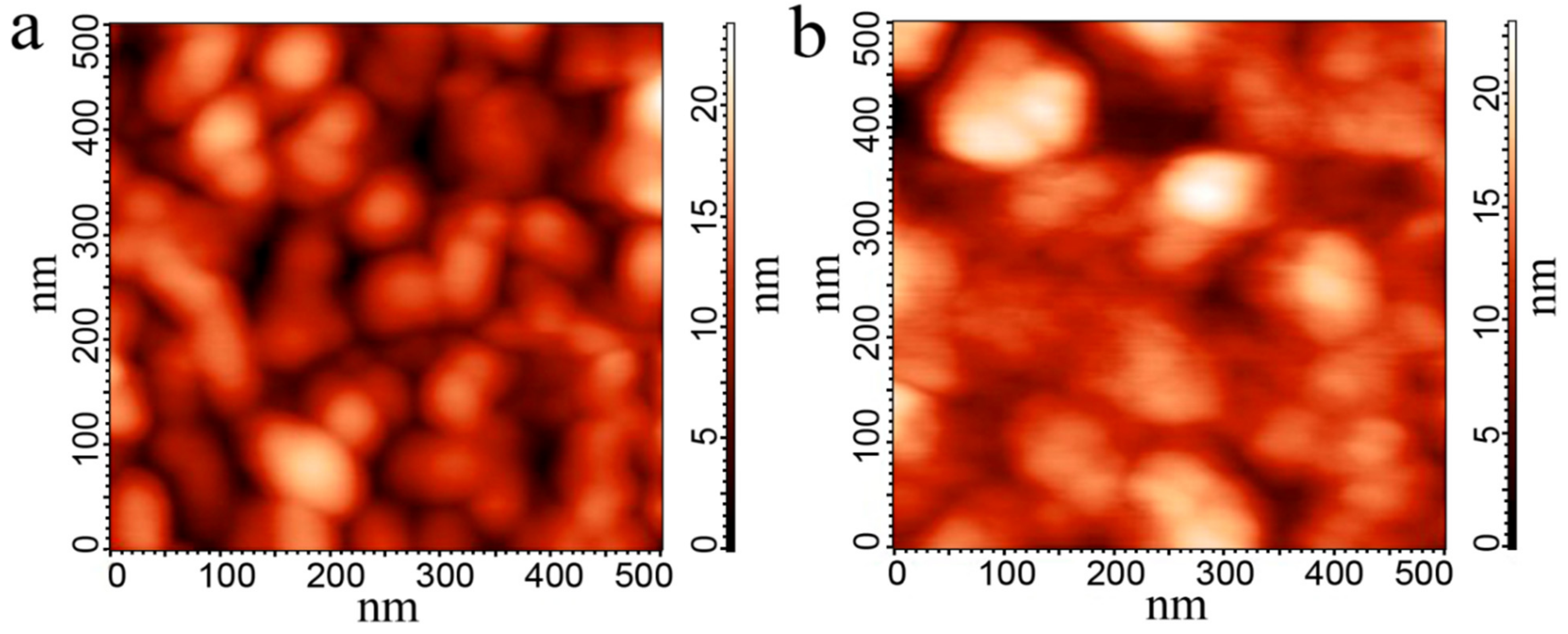
The structural and electric properties of the films were studied by means of atomic force microscopy (AFM), scanning electron microscopy (SEM), and the experimental complex for testing electric properties. The film and structure morphologies were examined on Hitachi SU8220 scanning electron microscopes at electron–beam energies ranging from 2 to 15 keV. A Solver PRO NT-MDT scanning microscope was used for obtaining the AFM images of substrate and sample surfaces and for measuring the film thicknesses. The measurements were carried out in contact and semi-contact modes. The AFM probe tip rounding radius was ~10 nm.
To visualize fluorinated graphene in the active layer, such AFM measurement modes as MAG and MAGSin were used. The signal associated with the probe phase is proportional to the product of the alternating signal amplitude at the modulation frequency (MAG is a signal proportional to the amplitude of cantilever oscillations) multiplied on the sinus of the cantilever oscillations phase shift relative to the reference signal. Accordingly, the phase shift value of the cantilever oscillations relative to the reference signal consists of the sum of the excitation signal phase shift relative to the reference and the cantilever oscillations phase shift relative to the excitation signal accurate to a certain “hardware” constant. The oscillation phase is more sensitive, in comparison with the amplitude, to changes in the interaction of the probe and the surface, and in particular to changes with local differences in the surface adhesion and viscoelasticity.
The film sheet resistance was studied with the use of four-probe JANDEL equipment and an HM21 Test Unit. For measuring current-voltage (I–V) characteristics, a Keithley picoamperemeter (model 6485) was used. Pulsed measurements were recorded on oscilloscope Keysight DSOX3012T.
The films and the structures were fabricated by the 2D printing method. A Dimatix FUJIFILM DMP-2831 printer equipped with a DMC-11610 printing head with 16 nozzle carriers of about 20-μm in diameter was used for printing. The printing process was implemented on both solid and flexible substrates. As flexible substrates, polyethylene terephthalate (PET) substrates with an adhesive coating (Lamond) and thickness of ~200-μm were used. During the printing process, the substrate temperature was maintained at 60 °C.
4. Discussion
Unexpected technological approaches often allow one to obtain promising solutions for the development of the new-generation devices in a wide spectrum of applications (for instance, [
6,
17,
18]).
In recent years, much attention has been paid to the studies related to nanostructure irradiation with various ion beams. The interest in these studies is associated not only with obtaining fundamental knowledge about the processes of radiation damage and its evolution in nanostructured objects but also with the practical application of ionizing radiation for the possibility of directed modification of the properties of nanostructures. The theory of properties nanomaterial modification by ionizing radiation is based on the theory of a thermal peak arising from the interaction of an incident ion with a substance and the subsequent energy transfer to the electron and nuclear subsystems for very short periods, thereby causing a sharp temperature increase in the structure, comparable, in some cases, with the material melting point. The distinctive feature of ion radiation from a similar thermal effect is that the modification of the properties of nanostructures during irradiation occurs locally along the entire path of ions in the material, while, during the thermal annealing, changes occur throughout the material bulk [
19].
In two-dimensional materials, the tuning of intrinsic material properties inevitably occurs through modifications on the atomic scale. Thus, 2D material science deals with defect engineering in the widest sense, that is, with the possibility of controlled removal, ddition, or manipulation of atoms, and as such, represents the key to unlocking the full potential for applications [
20]. Ion irradiation, with the possibility of controlled introduction of energy ions, provides an alternative simple top-down route for graphene modifications and the formation of graphene quantum dots [
21,
22,
23,
24].
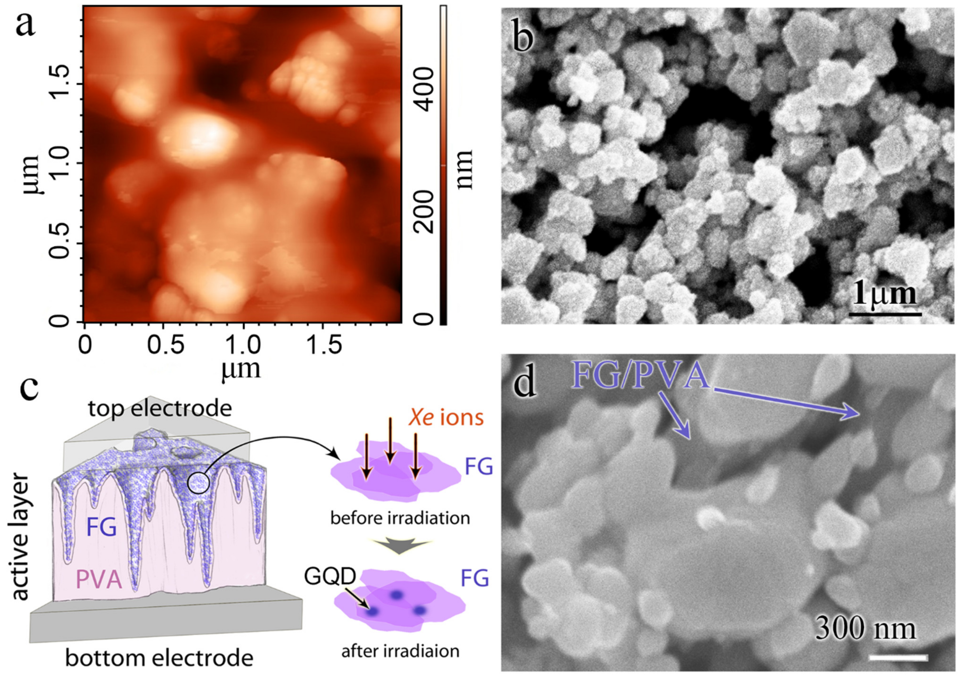
We assume that the formation of GQDs took place in the ion track areas. As mentioned above, when the ion passed through the film, a large amount of heat (up to 1500–3000 °C) was released locally in the few-nanometer size tracks for a short time (~10
−12–10
−11 s) [
25]. This local heating leads to the defluorination process. The images of GQDs obtained with the use of HREM are given in (
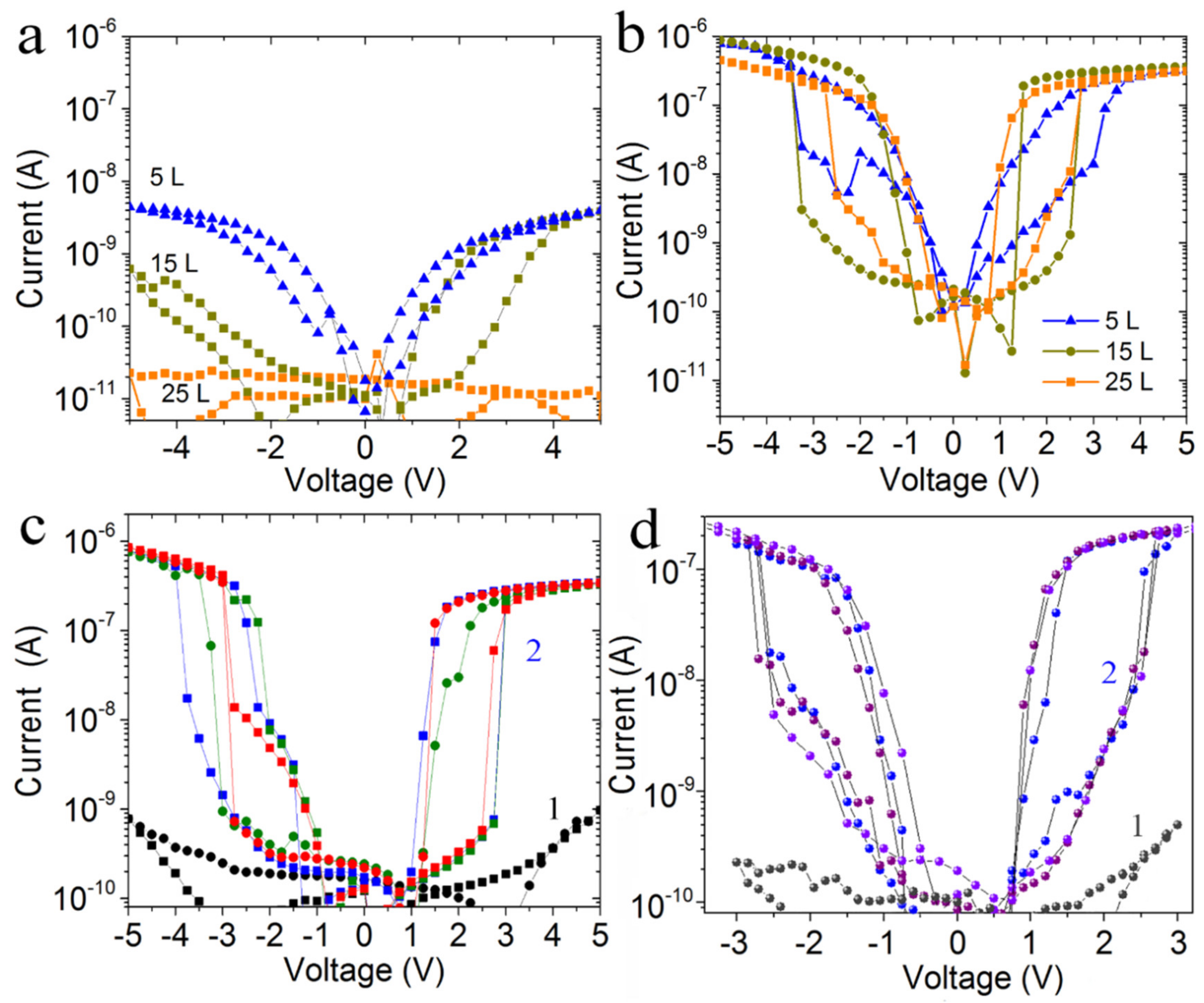
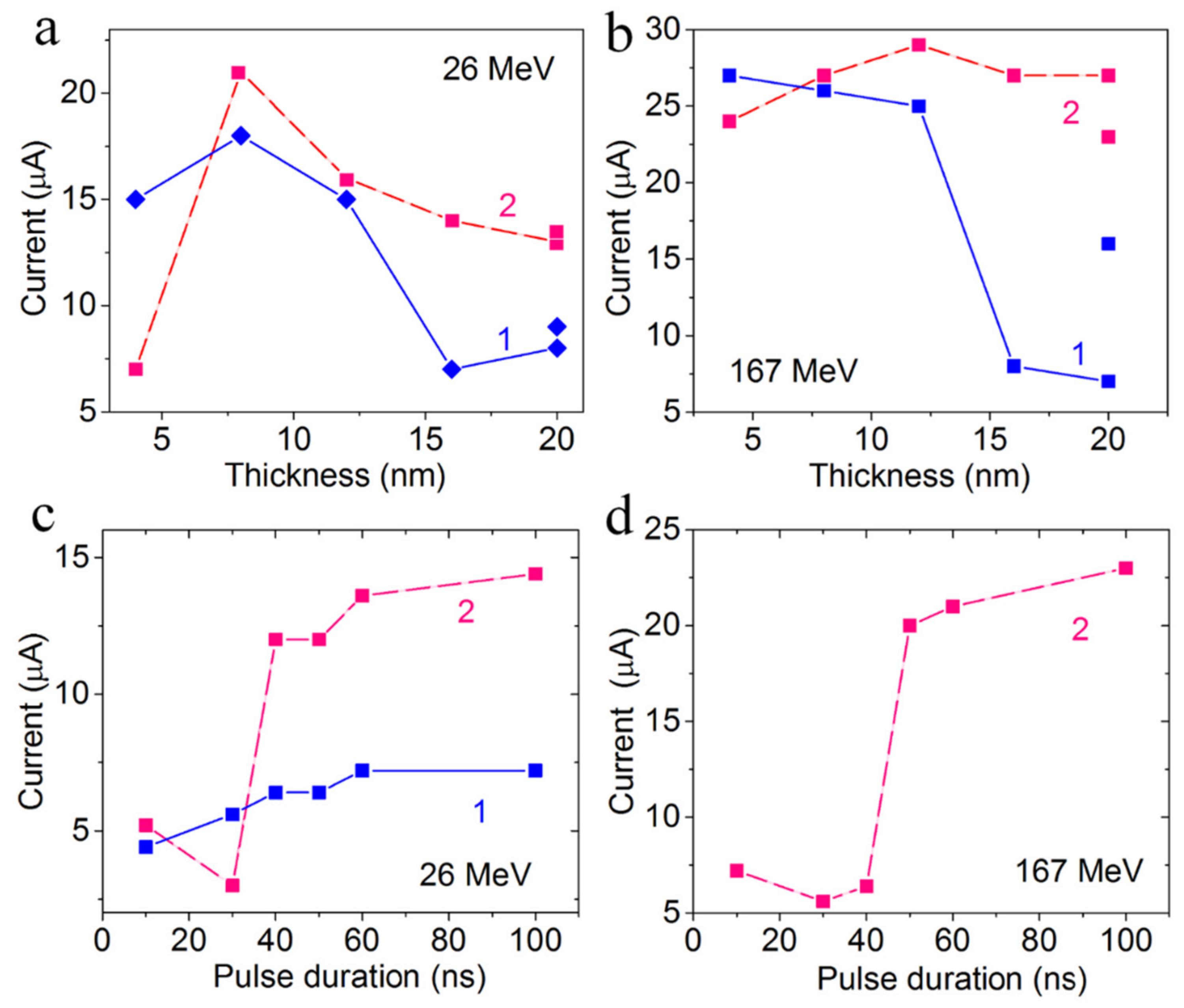
Supplementary Figure S2). The FG film thickness was varied from 4 to 20 nm. We suggest the formation of a vertically ordered system of GQDs in tracks, which leads to weak dependence of currents in irradiated crossbar structures (see
Figure 8a,b) for FG thickness range of 4–12 nm due to overcoming of the percolation threshold already at an ion dose of 3 × 10
10 cm
−2. For higher FG thickness, a decrease in current is most likely connected with the suppressing of fluorite removal when going deeper into the film.
According to the data presented above, the irradiation by Xe ions with an energy of 26–167 MeV and fluences of 3 × 10
10 cm
−2 and 3 × 10
11 cm
−2 changes the structure of active layers (formation of GQDs, fragmentation of the particles) and introduces some active centers, which leads to the observation of resistive switchings. The observation of resistive switchings after irradiation is the main finding of the present research. Based on our previous study [
16], we can state that, due to defluorination, ion irradiation leads to the formation of graphene quantum dots in FG, and, most likely, electrically active centers in PVA or at the FG–PVA interface. This observation correlates with the known data in that chalcogenide atoms are easily removed from a 2D material (MoS
2) upon irradiation due to the lower binding energy of chalcogenide atoms compared to transition metal atoms [
20,
26].
The mechanisms of the resistance-change phenomenon can be classed into two main types. The first one connects with the resistive switchings due to the formation/disintegration of conductive channels or filaments with different origins [
5,
9]. The second type of switching mechanism implies the participation of some electrically active centers (GQDs and traps) that can change their conductivity under applied voltage [
12]. In the last case and in our materials, the open state current depends on the area of the structure due to variation in the number of conductive passes formed in structures. Thus, the resistive switching effect in our structures has described the conduction over quantum dots proceeding with the participation of active traps at the GQDs–PVA interface. GQDs provide the permanent conductive part of the pathways, whereas the traps at the GQDs–PVA interface are activated/deactivated only upon the applied voltage [
12].
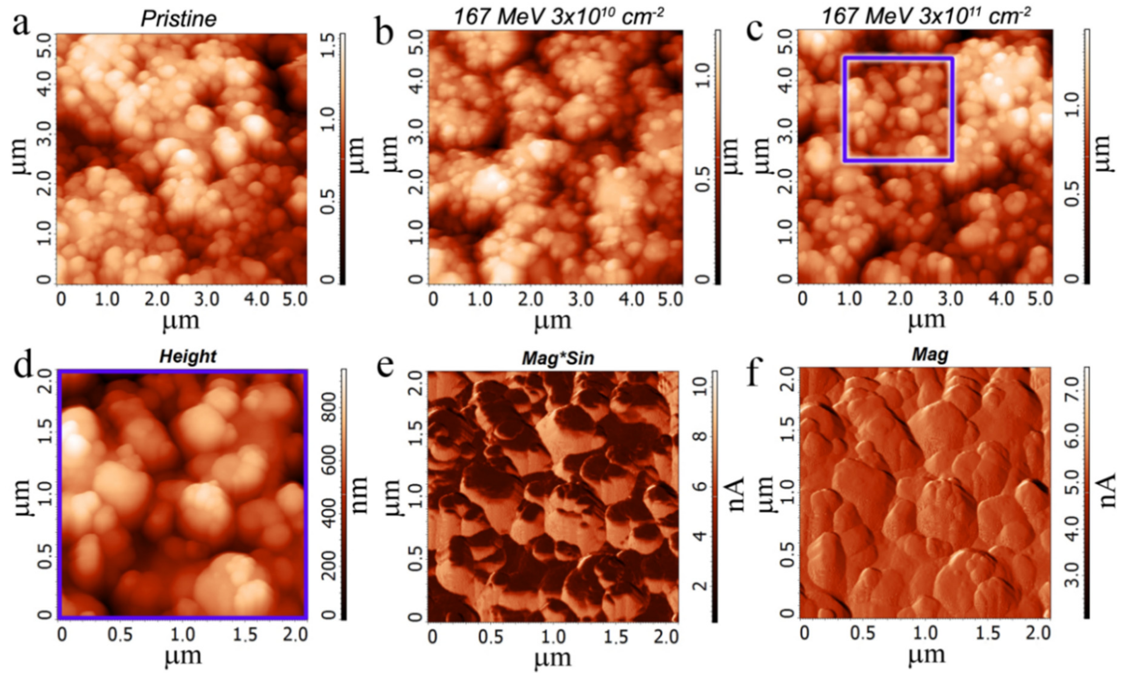
As is shown in
Figure 3, the ion irradiation leads to the formation of thermally expanded flakes with a size of ~100 nm and cracking of the FG flakes on small particles with an ion energy increase. The appearance of small (~3 nm) graphene quantum dots embedded in FG nanoparticles is also expected in the irradiated films, according to our previous study [
16]. After the Xe ions irradiation with both energies (26 and 167 MeV) and fluences (3 × 10
10 and 3 × 10
11 cm
−2), the resistive switchings were observed in all irradiated structures. The ON/OFF current ratios practically in all cases were 2–4 orders of magnitude regardless of the FG layer thickness. The current values in the crossbar structures are increased from 10
−11–10
−9 A to 10
−7–10
−6 A. It is worth mentioning that, after irradiation, the PVA film (without FG layer) does not show any conductivity or resistive switchings.
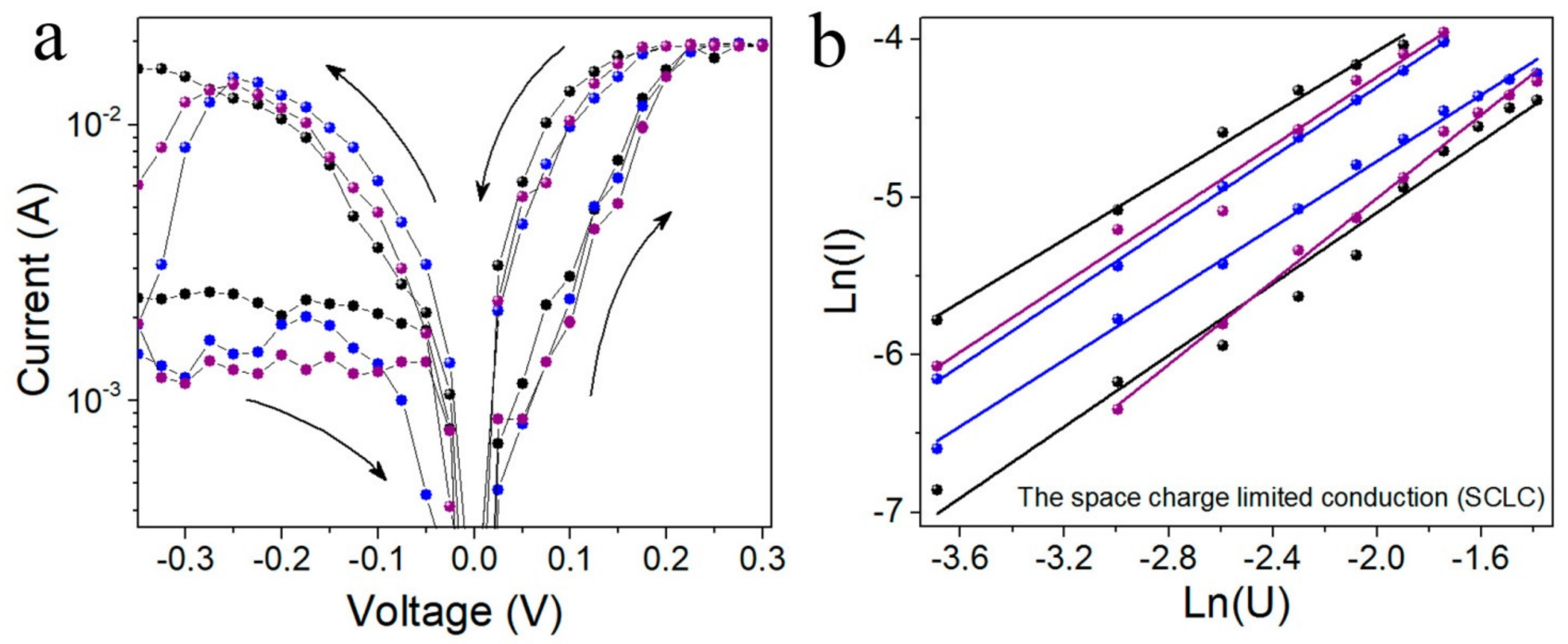
At the current-voltage characteristics in coordinates ln(I) versus ln(V) corresponding to the space charge limited conduction (SCLC) for crossbar structures, a linear fitting is observed. The same conductive mechanism was found for the case of Ag–FG–PVA–Ag crossbar structures with the FG–PVA active layer, in which GQDs are formed due to low fluorination [
12]. SCLC is connected with the carrier tunneling between the traps. These traps are suggested to be related to GQDs in the FG matrix. The barrier height at the GQDs–FG interface was estimated in [
17] as 0.48–0.50 eV for the similar FG layers. These values can be varied depending on the GQD size. For small GQDs (3–5 nm), the barrier height is strongly decreased. Practically the same slope (1.0–1.3) of all curves means that the traps involved in the conduction do not change.
In our study, the resistive switching mechanism is most likely associated with the activation with an applied voltage of the localized states at the FG–PVA interface, which, in turn, leads to the formation of paths for the electric current flow between the GQDs. Thus, on the one hand, PVA plays the role of a porous framework. On the other hand, PVA is involved in the surface states formation because it increases the ON/OFF current ratio. The strong current increase in the open state is associated with the percolation transition in the active layer, i.e., with the appearance of current paths after the voltage application.
One more interesting finding is connected with the fact that the current in the open state is very weak depending on the FG thickness in the studied range of fluences and energies. We have suggested that the GQDs formed in one ion track under irradiation have good electric connections or one GQD multilayer with a thickness up to ~10 nm is formed due to irradiation. Thus, in [
27], the possibility of stitching individual graphene sheets into a common three-dimensional structure using ion irradiation was shown, and according to [
28], the passage of heavy Au ions through the PMMA–graphene–Cu trilayer structure leads to creating rectilinear damage zones, the so-called latent tracks, all along the ion trajectory in the structure.
It was demonstrated that FG–PVA crossbar structures have good flexibility [
12]. The currents in open and closed states are not practically changed up to the tensile strain due to the structure bending up to 6.5%. For a higher strain (6.5–8%), the ON/OFF ratio is decreased. Thus, the considered structures with the active FG–PVA layer are perspectives for the development of flexible memristors. The use of 2D printed technologies to create these memristors allows one to elaborate on the cheap variant of flexible memristor technologies.

 ,
, 

