
Development of Actuators for Repairing Cracks by Coating W Wires with Reactive Multilayers

 , and
, and 
Abstract
:
1. Introduction
2. Materials and Methods
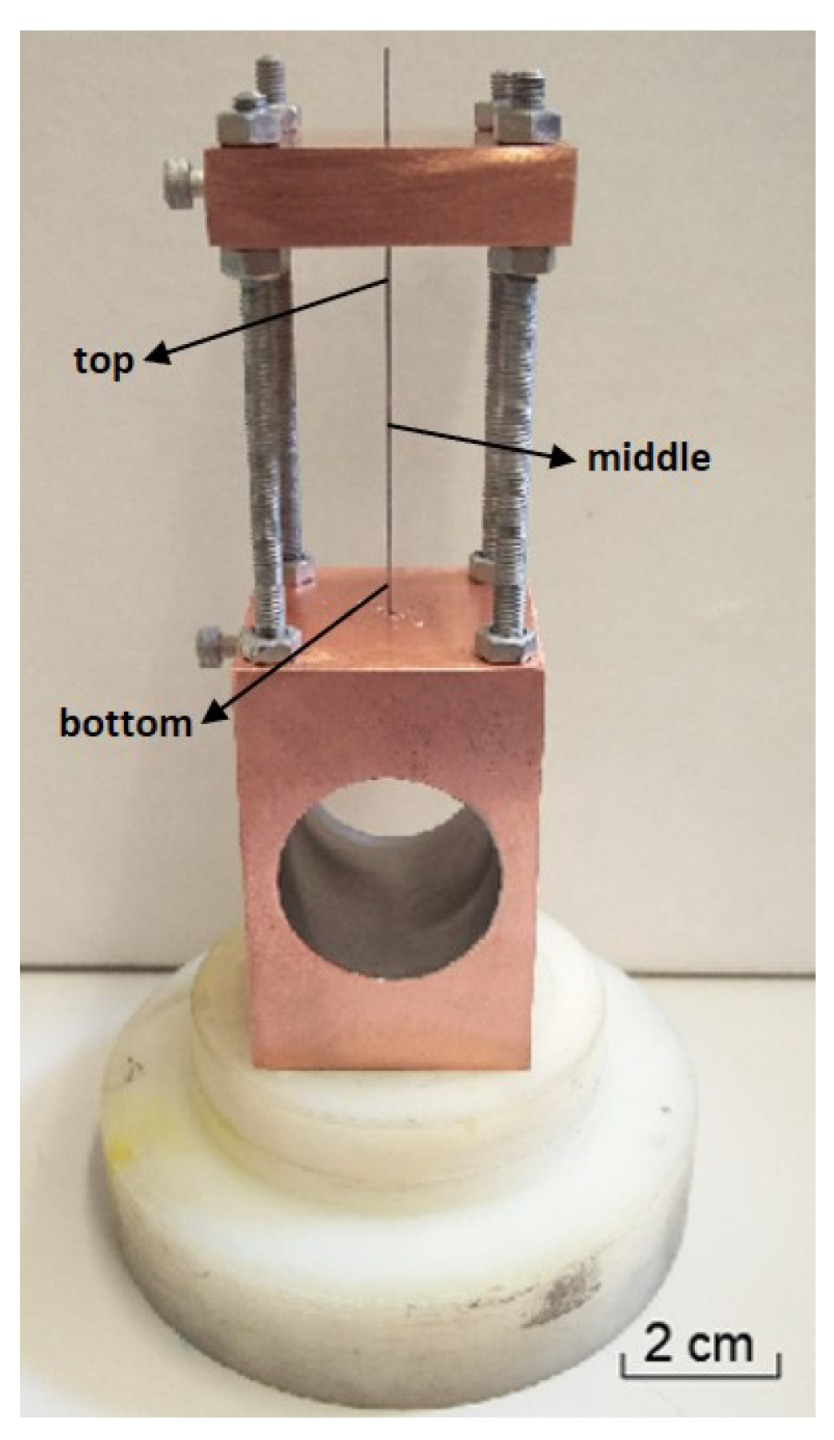
2.1. Deposition Technique
2.2. Characterization Techniques
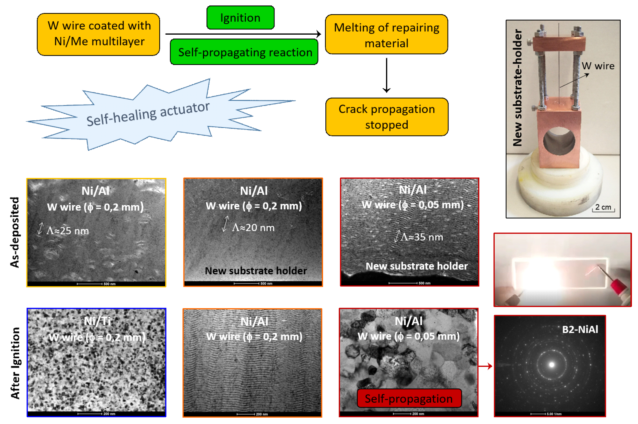
3. Results and Discussion
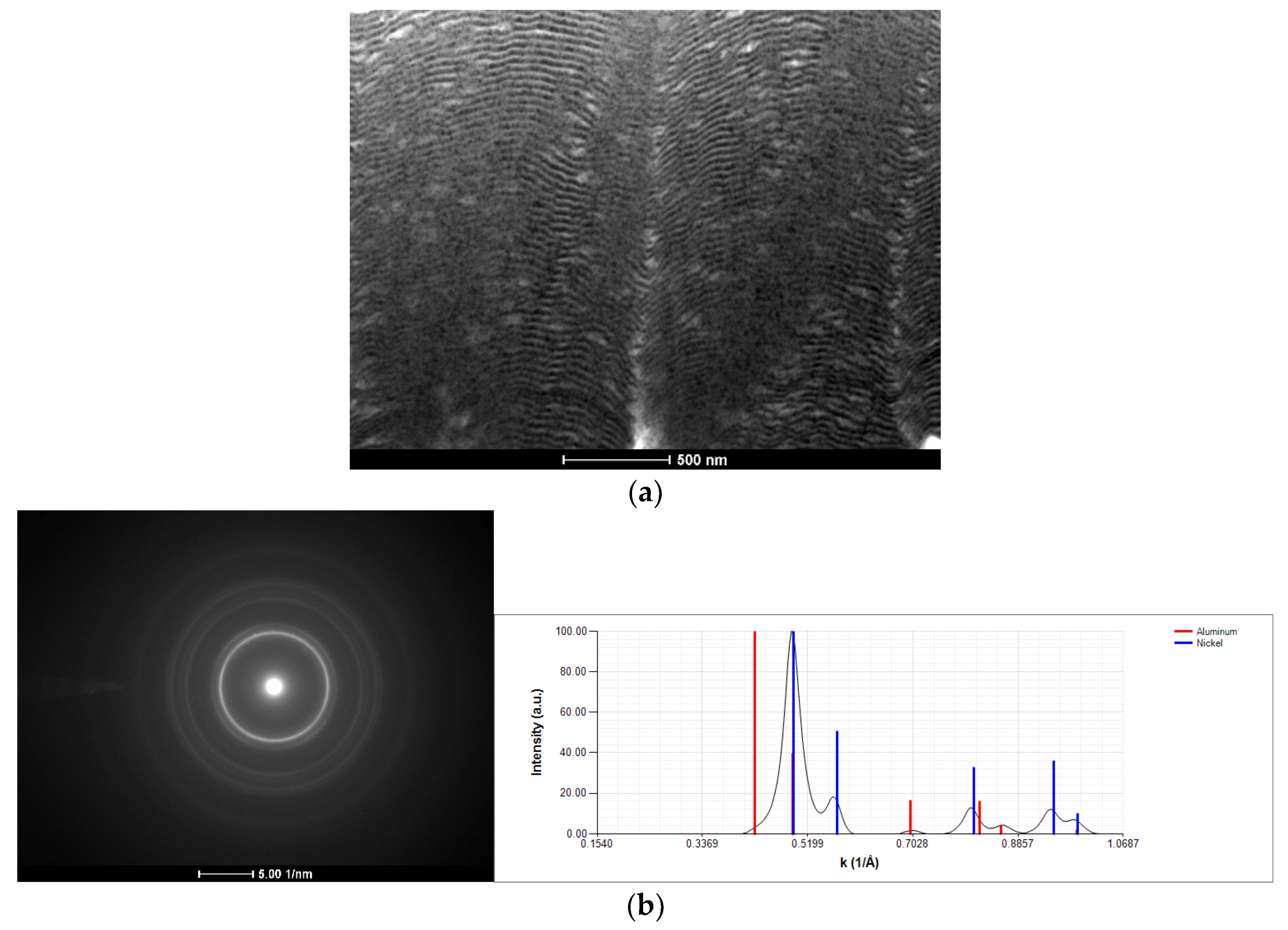
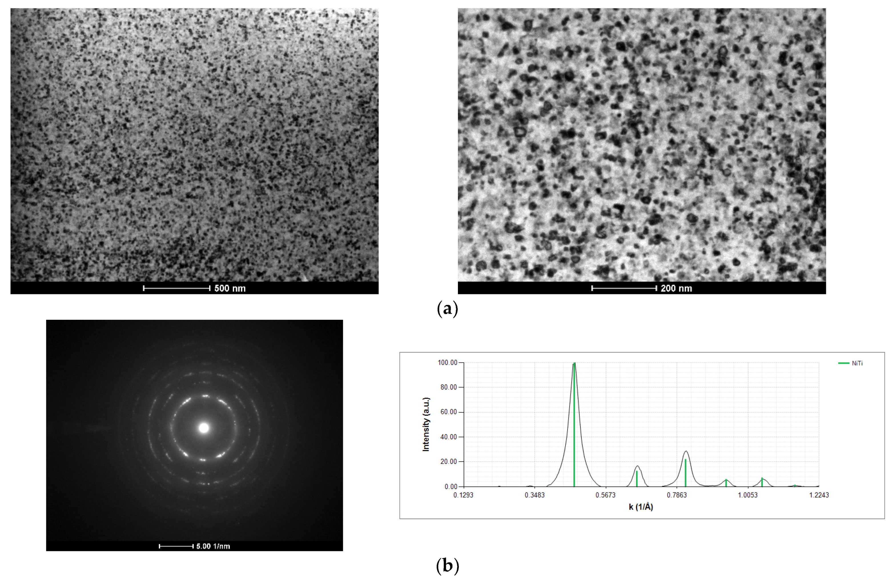
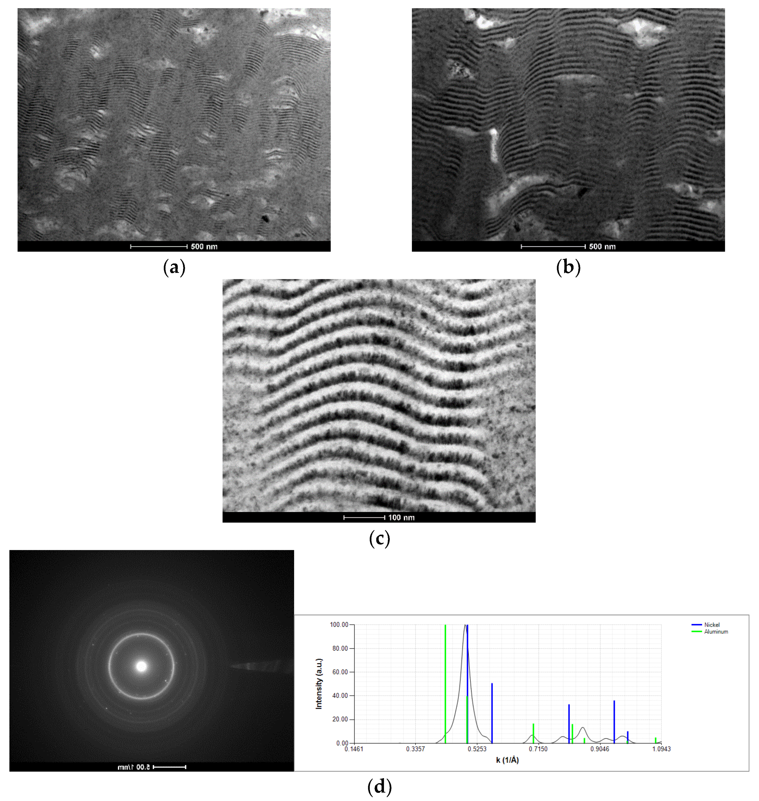
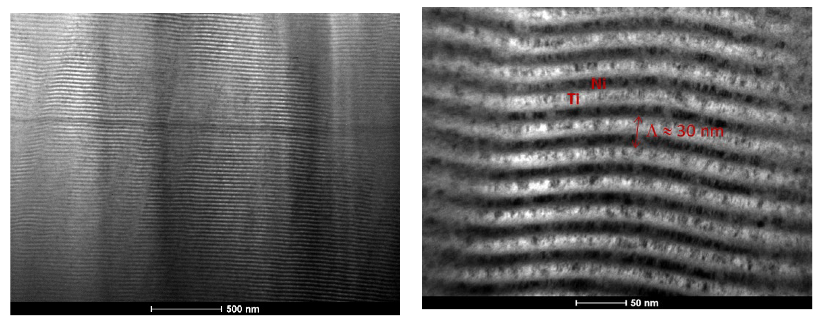
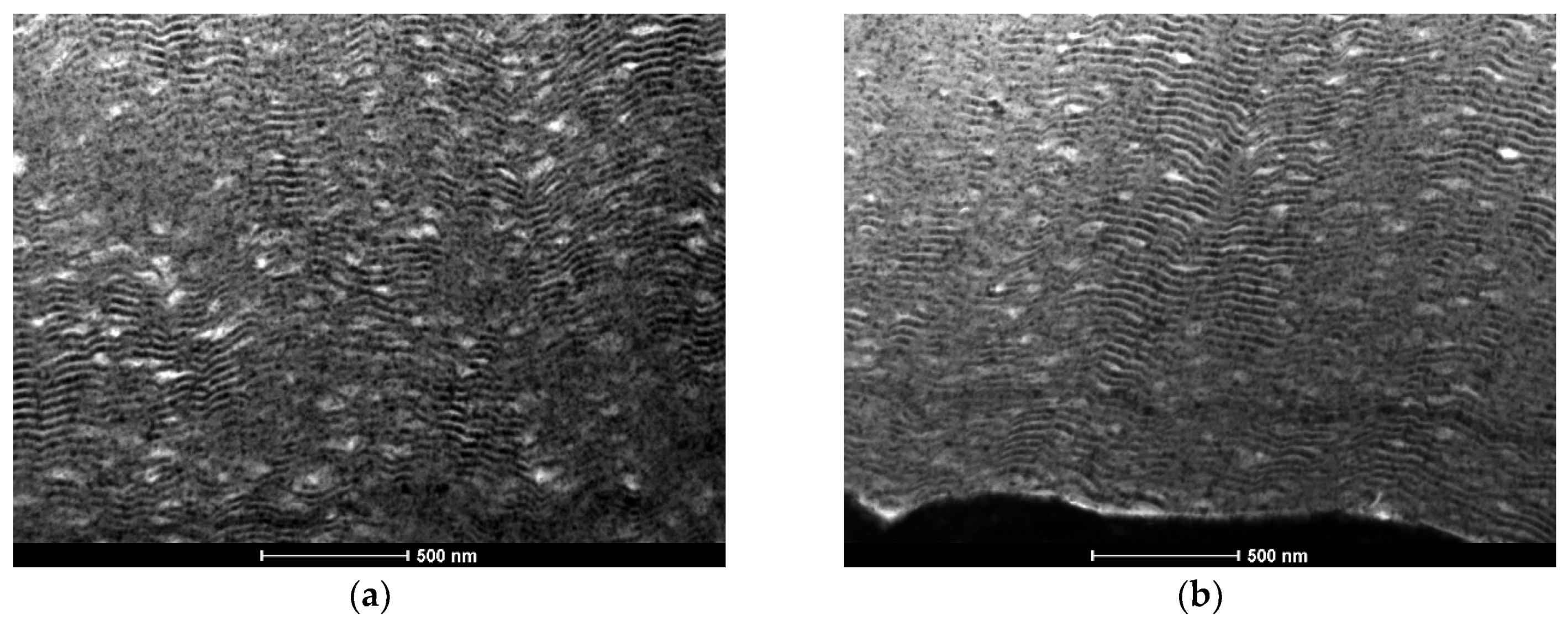
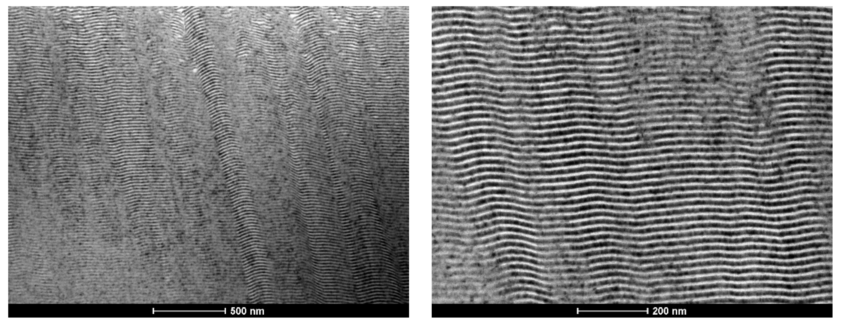
3.1. As-Deposited
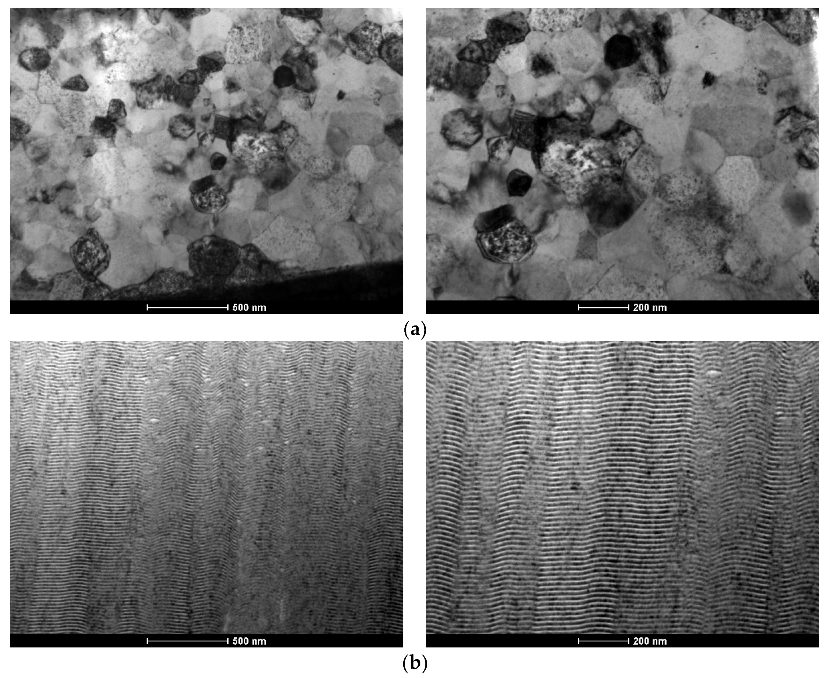
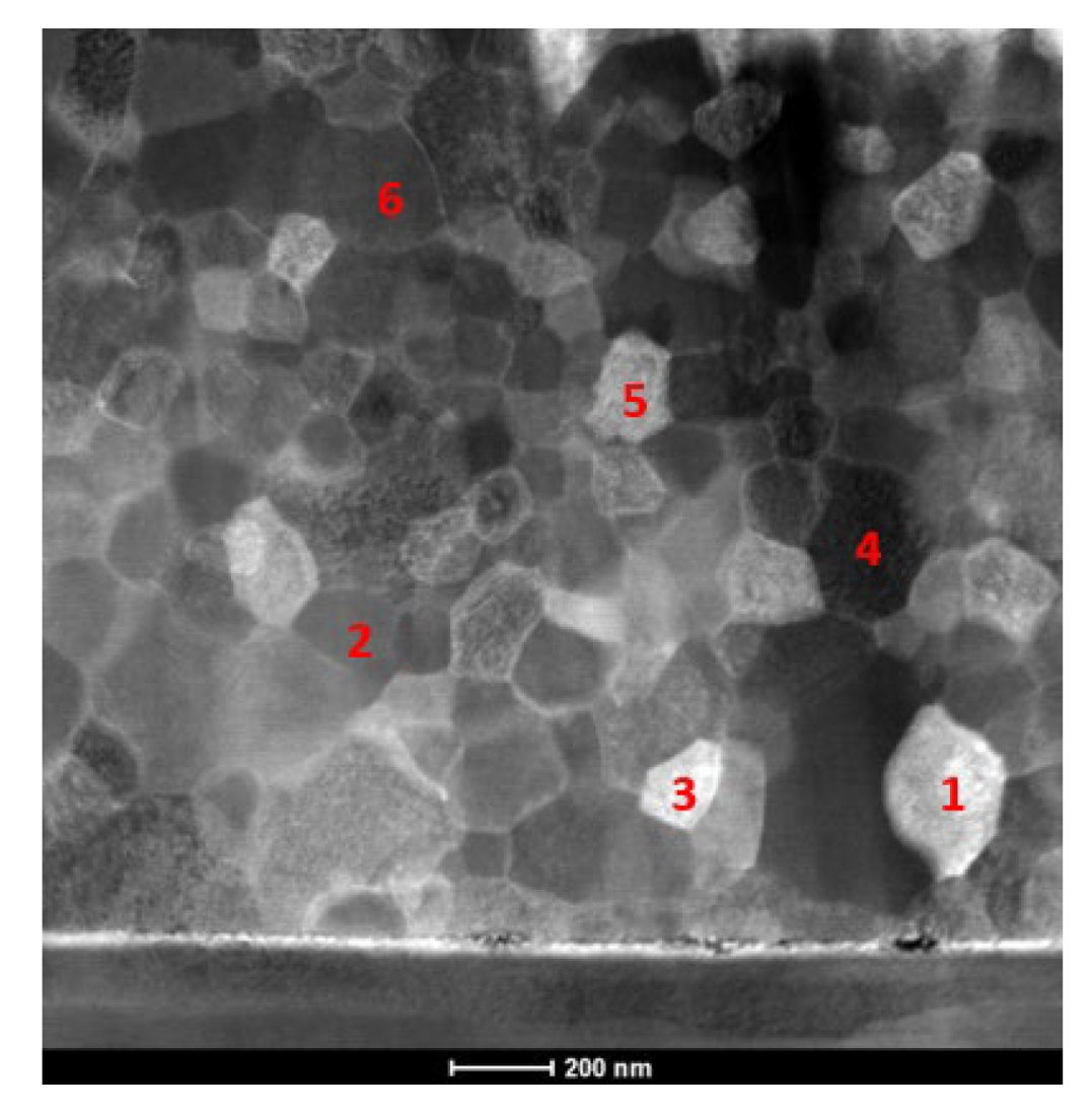
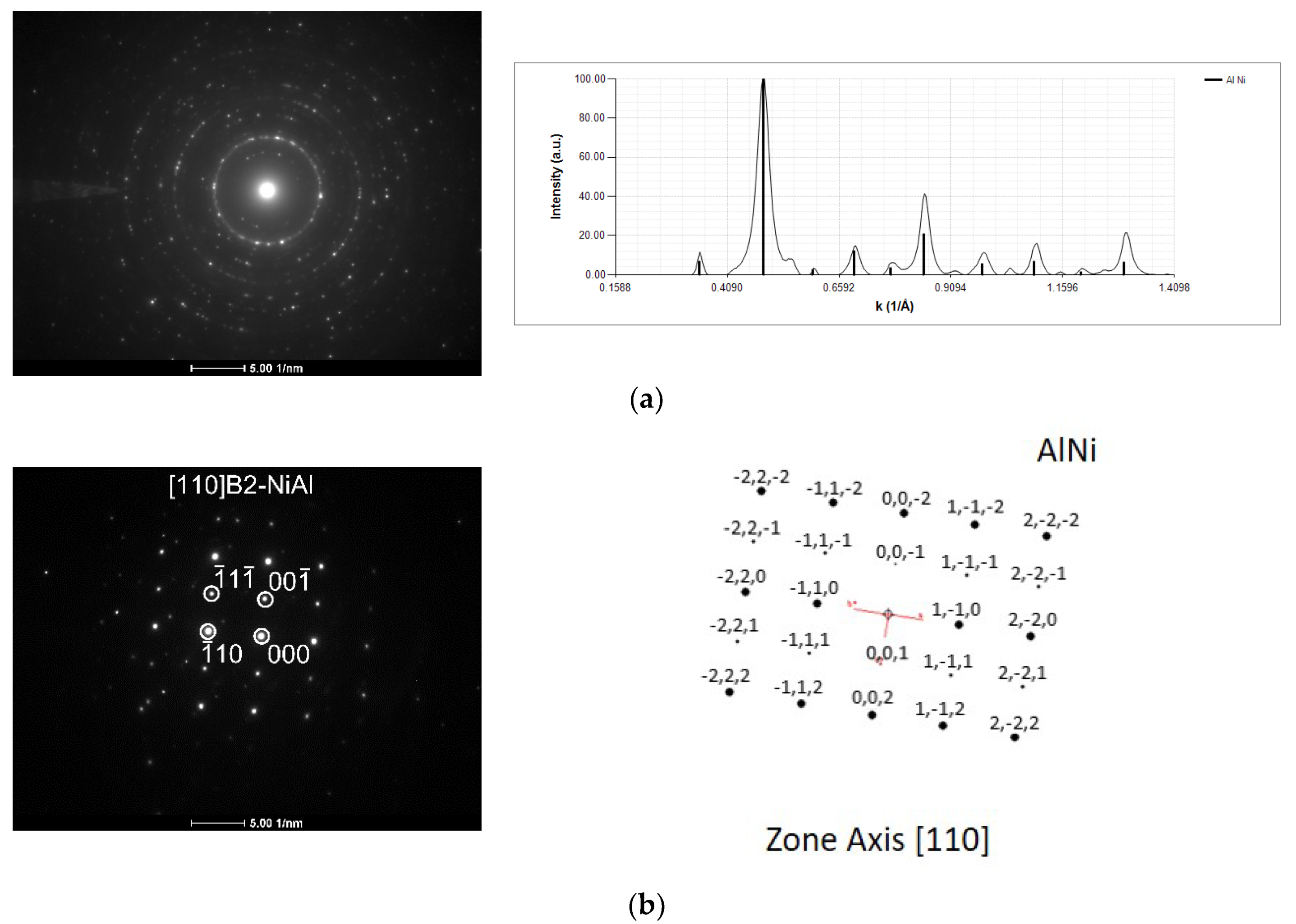
3.2. After Ignition
4. Conclusions
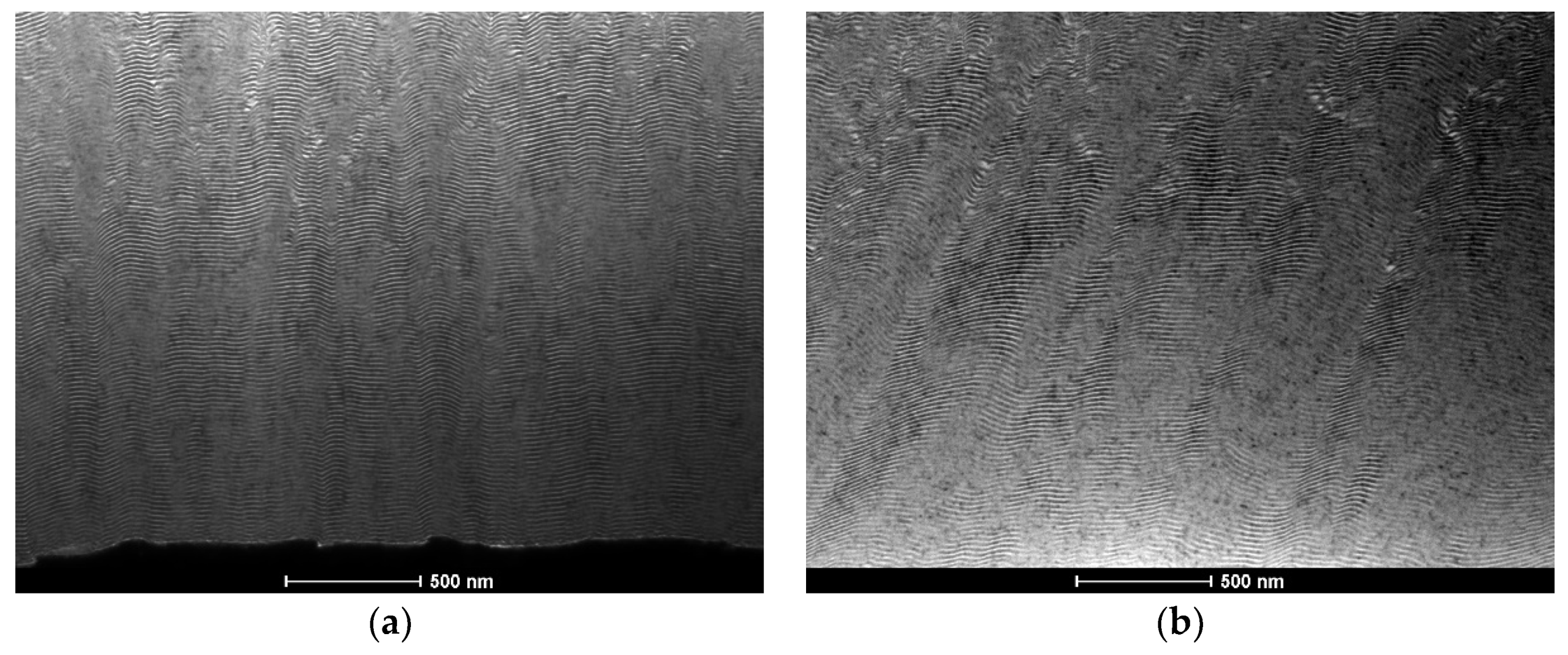
- The nanostructured character of as-deposited Ni/Me multilayer thin films onto tungsten wires was confirmed by TEM;
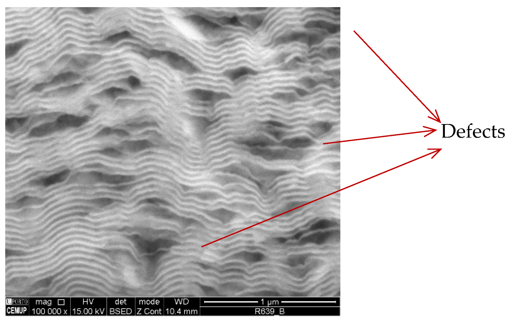
- The presence of Al-rich droplets is detected by TEM in Al/Ni multilayer thin films, especially if deposited onto the smallest diameter W wires (ϕ = 0.05 mm);
- The use of a new substrate holder allowed these defects to be reduced, and more homogeneous films were obtained throughout the entire length of the wires;
- In the case of the Ni–Ti system, defect-free multilayer thin films are deposited independently of the substrate holder, wire diameter, or modulation period;
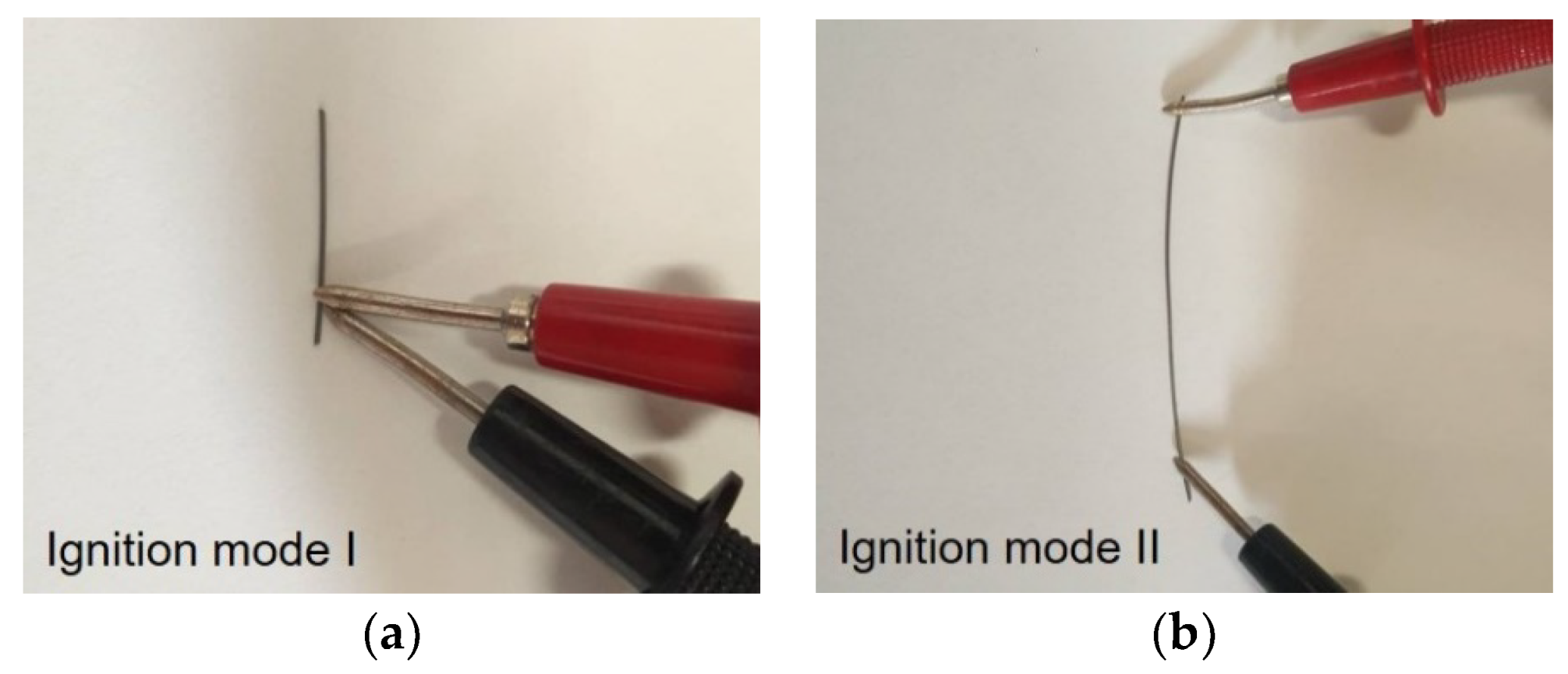
- Low energy Ni/Ti films present a fine grained microstructure, and the formation of the NiTi intermetallic phase occurred after several “shots” of ignition using mode I. However, self-propagation was not promoted;
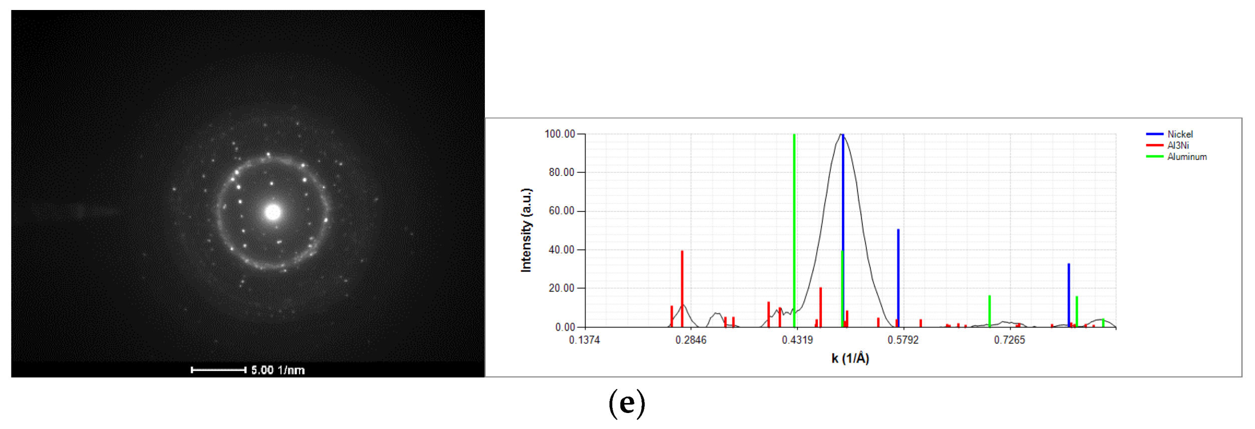
- Using the mode II ignition, a self-propagating reaction was triggered in a W wire (ϕ = 0.05 mm) coated with an Al/Ni multilayer thin film with a modulation period close to 20–30 nm;
- During the self-propagating reaction, the desired B2-AlNi intermetallic phase formed, according to the average chemical composition of the film.
Author Contributions
Funding
Institutional Review Board Statement
Informed Consent Statement
Data Availability Statement
Acknowledgments
Conflicts of Interest
References
- Dreizin, E.L. Metal-Based Reactive Nanomaterials. Prog. Energy Combust. Sci. 2009, 35, 141–167. [Google Scholar] [CrossRef]
- Weihs, T.P. Fabrication and Characterization of Reactive Multilayer Foils and Films. In Metallic Films for Electronic, Optical and Magnetic Applications—Structure, Processing and Properties, 1st ed.; Barmak, K., Coffey, K., Eds.; Woodhead Publishing Limited: Cambridge, UK, 2014; pp. 160–242. [Google Scholar] [CrossRef]
- Ramos, A.S.; Cavaleiro, A.J.; Vieira, M.T.; Morgiel, J.; Safran, G. Thermal stability of nanoscale metallic multilayers. Thin Solid Films 2014, 571, 268–274. [Google Scholar] [CrossRef]
- Colgan, E.G. A review of thin-film aluminide formation. Mater. Sci. Rep. 1990, 5, 1–44. [Google Scholar] [CrossRef]
- Ramos, A.S.; Vieira, M.T.; Morgiel, J.; Grzonka, J.; Simões, S.; Vieira, M.F. Production of intermetallic compounds from Ti/Al and Ni/Al multilayer thin films—A comparative study. J. Alloys Compd. 2009, 484, 335–340. [Google Scholar] [CrossRef]
- Adams, D.P. Reactive multilayers fabricated by vapor deposition: A critical review. Thin Solid Films 2015, 576, 98–128. [Google Scholar] [CrossRef] [Green Version]
- Adams, D.P.; Rodriguez, M.A.; McDonald, J.P.; Bai, M.M.; Jones, E., Jr.; Brewer, L.; Moore, J.J. Reactive Ni/Ti nanolaminates. J. Appl. Phys. 2009, 106, 093505. [Google Scholar] [CrossRef]
- Lehnert, T.; Grimmer, H.; Boni, P.; Horisberger, M.; Gotthardt, R. Characterization of shape-memory alloy thin films made up from sputter-deposited Ni/Ti multilayers. Acta Mater. 2000, 48, 4065–4071. [Google Scholar] [CrossRef]
- Cho, H.; Kim, H.Y.; Miyazaki, S. Fabrication and characterization of Ti-Ni shape memory thin film using Ti/Ni multilayer technique. Sci. Technol. Adv. Mater. 2005, 6, 678–683. [Google Scholar] [CrossRef]
- Wang, J.; Besnoin, E.; Duckham, A.; Spey, S.J.; Reiss, M.E.; Knio, O.M.; Powers, M.; Whitener, M.; Weihs, T.P. Room-temperature soldering with nanostructured foils. Appl. Phys. Lett. 2003, 83, 3987–3989. [Google Scholar] [CrossRef]
- Duckham, A.; Spey, S.J.; Wang, J.; Reiss, M.E.; Weihs, T.P.; Besnoin, E.; Knio, O.M. Reactive nanostructured foil used as heat source for joining titanium. J. Appl. Phys. 2004, 96, 2336–2342. [Google Scholar] [CrossRef]
- Qiu, X.; Wang, J. Bonding silicon wafers with reactive multilayer foils. Sens. Actuators A 2008, 141, 476–481. [Google Scholar] [CrossRef]
- Cao, J.; Feng, J.C.; Li, Z.R. Microstructure and fracture properties of reaction-assisted diffusion bonding of TiAl intermetallic with Al/Ni multilayer foils. J. Alloys Compd. 2008, 466, 363–367. [Google Scholar] [CrossRef]
- Cavaleiro, A.J.; Ramos, A.S.; Braz Fernandes, F.M.; Schell, N.; Vieira, M.T. Follow-up structural evolution of Ni/Ti reactive nano and microlayers during diffusion bonding of NiTi to Ti6Al4V in a synchrotron beamline. J. Mater. Process. Technol. 2020, 275, 116354. [Google Scholar] [CrossRef]
- Rabinovich, O.S.; Grinchuk, P.S.; Andreev, A.M.; Khina, B.B. Conditions for combustion synthesis in nanosized Ni-Al films on a substrate. Phys. Rev. B 2007, 392, 272–280. [Google Scholar] [CrossRef]
- Ramos, A.S.; Maj, L.; Morgiel, J.; Vieira, M.T. Coating of Tungsten Wire with Ni/Al Multilayers for Self-Healing Applications. Metals 2017, 7, 574. [Google Scholar] [CrossRef] [Green Version]
- Edelstein, A.S.; Everett, R.K.; Richard, G.Y.; Qadri, S.B.; Altman, E.I.; Foley, J.C.; Perepezko, J.H. Intermetallic phase formation during annealing of Al/Ni multilayers. J. Appl. Phys. 1994, 76, 7850–7859. [Google Scholar] [CrossRef] [Green Version]
- Liu, B.; Yu, X.; Jiang, X.; Qiao, Y.; You, L.; Wang, Y.; Ye, F. Effect of deposition substrates on surface topography, interface roughness and phase transformation of the Al/Ni multilayers. Appl. Surf. Sci. 2021, 546, 149098. [Google Scholar] [CrossRef]
- Kittell, D.E.; Yarrington, C.D.; Hobbs, M.L.; Abere, M.J.; Adams, D.P. A diffusion-limited reaction model for self-propagating Al/Pt multilayers with quench limits. J. Appl. Phys. 2018, 123, 145302. [Google Scholar] [CrossRef]
- Kang, B.C.; Kim, H.Y.; Kwon, O.Y.; Hong, S.H. Bilayer thickness effects on nanoindentation behavior of Ag/Ni multilayers. Scr. Mater. 2007, 57, 703–706. [Google Scholar] [CrossRef]
- Ramos, A.S.; Simões, S.; Maj, L.; Morgiel, J.; Vieira, M.T. Effect of deposition parameters on the reactivity of Al/Ni multilayer thin films. Coatings 2020, 10, 721. [Google Scholar] [CrossRef]
- Lima, P.C.; Rodrigues, P.F.; Ramos, A.S.; Costa, J.D.M.; Braz Fernandes, F.M.; Vieira, M.T. Experimental Analysis of NiTi Alloy during Strain-Controlled Low-Cycle Fatigue. Materials 2021, 14, 4455. [Google Scholar] [CrossRef]
- Knepper, R.; Snyder, M.R.; Fritz, G.; Fisher, K.; Knio, O.M.; Weihs, T.P. Effect of varying bilayer spacing distribution on reaction heat and velocity in reactive Al/Ni multilayers. J. Appl. Phys. 2009, 105, 083504. [Google Scholar] [CrossRef]
- Cavaleiro, A.J.; Santos, R.J.; Ramos, A.S.; Vieira, M.T. In-situ thermal evolution of Ni/Ti multilayer thin films. Intermetallics 2014, 51, 11–17. [Google Scholar] [CrossRef]
- Cho, H.; Kim, H.Y.; Miyazaki, S. Alloying process of sputter-deposited Ti/Ni multilayer thin films. Mater. Sci. Eng. A 2006, 438–440, 699–702. [Google Scholar] [CrossRef]
- Monroe, P.R.; Baker, I. Effect of Accelerating Voltage on Planar and Axial Channeling in Ordered Intermetallic Compounds. J. Mater. Res. 1992, 7, 2119–2125. [Google Scholar] [CrossRef]


| Point | Al [at.%] | V [at.%] | Ni [at.%] |
|---|---|---|---|
| 1 | 42.4 | 3.6 | 54.0 |
| 2 | 41.0 | 4.4 | 54.6 |
| 3 | 36.0 | 4.0 | 60.0 |
| 4 | 41.3 | 5.0 | 53.7 |
| 5 | 40.4 | 4.4 | 55.2 |
| 6 | 37.4 | 5.0 | 57.6 |
Publisher’s Note: MDPI stays neutral with regard to jurisdictional claims in published maps and institutional affiliations. |
© 2022 by the authors. Licensee MDPI, Basel, Switzerland. This article is an open access article distributed under the terms and conditions of the Creative Commons Attribution (CC BY) license (https://creativecommons.org/licenses/by/4.0/).
Share and Cite
Santos Silva, G.; Maj, L.; Morgiel, J.; Vieira, M.T.; Ramos, A.S. Development of Actuators for Repairing Cracks by Coating W Wires with Reactive Multilayers. Materials 2022, 15, 869. https://doi.org/10.3390/ma15030869
Santos Silva G, Maj L, Morgiel J, Vieira MT, Ramos AS. Development of Actuators for Repairing Cracks by Coating W Wires with Reactive Multilayers. Materials. 2022; 15(3):869. https://doi.org/10.3390/ma15030869
Chicago/Turabian StyleSantos Silva, Gabriel, Lukasz Maj, Jerzy Morgiel, Maria Teresa Vieira, and Ana Sofia Ramos. 2022. "Development of Actuators for Repairing Cracks by Coating W Wires with Reactive Multilayers" Materials 15, no. 3: 869. https://doi.org/10.3390/ma15030869
APA StyleSantos Silva, G., Maj, L., Morgiel, J., Vieira, M. T., & Ramos, A. S. (2022). Development of Actuators for Repairing Cracks by Coating W Wires with Reactive Multilayers. Materials, 15(3), 869. https://doi.org/10.3390/ma15030869