2. Statement of the Problem
To estimate the radiation resistance of semiconductors at a relatively low level of compensation, the parameter
ηe is often used, that is, the removal rate of carriers under the irradiation influence (see, for example, [
4,
5]):
where
n0 is the electron concentration in the semiconductor before irradiation,
n is the electron concentration after irradiation, and
Φ is the fluence (for certainty, we will consider the n-type conductivity material).
In wide-gap semiconductors (i.e., SiC, GaN, AlGaN, Ga
2O
3), at the current level of technology, there are always deep centers (levels) that are practically not ionized at room temperature. When heated, the degree of their ionization increases, which leads to a temperature dependence of the measured
ηe value [
6]. It should also be noted that, in determining the
ηe value, the concentration of uncompensated donors,
Nd −
Na, is often used instead of the
n value. In current
n-type device-quality SiC, prior to irradiation, the concentration of carriers at room temperature can be considered equal with acceptable accuracy to the concentration of shallow donor
Nd (nitrogen). Irradiation with protons and/or electrons creates acceptor-type levels in the band gap [
7,
8]. As long as the total concentration of acceptor levels created by irradiation,
, is less than the initial carrier concentration
n0, the residual electron concentration in the conduction band can be considered equal to
n =
n0 −
. However, at
>
n0, the shallow donor level responsible for the initial electron concentration in the non-irradiated semiconductor turns out to be completely empty, and the “residual” electron concentration
n is determined by the generation of electrons from deep levels.
The
η value can critically depend on the method of measurement. In the case of measuring current-voltage (
I–V) characteristics or the Hall effect, the electron concentration after irradiation
n is directly determined from the measurements. The value of
n is determined directly, in this case, at any levels of compensation, including large fluences
Φ, when expression (1) becomes inapplicable. When measuring capacitance-voltage characteristics (
C–V measurements), carried out on reverse-biased Schottky diodes or p-n junctions, the
Nd − Na value is measured. In this case, the removal rate
ηN (also at a relatively low level of compensation) is defined as:
where (
Nd −
Na)
0 is the initial value of the concentration of uncompensated donors, and (
Nd −
Na)
1 is the (
Nd −
Na) value after irradiation.
Properly speaking, the degree of deep centers filling in the I–V (or the Hall effect) measurements and C–V measurements is always different. The quasi-neutral situation is realized when measuring the I–V characteristics. Then, the filling of the level is determined by two processes: thermal emission of electrons from the corresponding center, and recapture from the conduction band (C-band) to the level. If the level at the measurement temperature lies above the Fermi level, then it is empty; below it, it is filled.
In C–V measurements, the levels at which electrons are captured as a result of irradiation are located in the space charge layer, where there are practically no electrons in the C-band, and the carrier concentration at the level is determined by thermal emission from the level. At long measurement times, all levels lying in the upper half of the band gap should be emptied. However, for sufficiently deep levels, the time for complete depletion can be extremely long and significantly exceed the practically acceptable measurement time.
If the acceptor level is formed during irradiation in the lower half of the band gap, it will be filled with electrons, charged negatively, and will contribute to both a decrease in the Nd − Na value and a decrease in the concentration n.
If an acceptor level is formed in the upper half of the band gap, then it will reduce the n value. However, the decrease in the value of Nd − Na will depend on its depth (ionization energy). If the level ionization energy is large enough (deep level), then in a reasonable time for C–V measurements, it can remain almost completely filled with electrons. In this case, this level will contribute to the measured Nd − Na value. However, a relatively shallow level in C–V measurements can be completely emptied in a time much shorter than the measurement time already at room temperature. In this case, such a level will not contribute to the measured Nd − Na value.
Measurements of current-voltage and
C–V characteristics of SiC Schottky diodes irradiated with protons and electrons were made in the Ref. [
9]. Both types of irradiation lead to an increase in the resistance of the diode base. With large radiation doses, the resistance of the sample base increases extremely sharply, and measuring the
I–V characteristics allows to trace the change in electron concentration by many orders of magnitude.
The value of
Nd −
Na, determined from the capacitance–voltage characteristics at the same irradiation level, decreases at a much weaker rate [
10,
11]. In addition, since levels with different ionization empty at different rates, the measured
C–V characteristics significantly depend on the measurement frequency and are characterized by a noticeable frequency dispersion at a given irradiation level [
11].
The above considerations can be clearly illustrated using a simple qualitative model.
3. Qualitative Model
It is known that a number of deep levels are formed in silicon carbide under the actions of electron and proton irradiation [
9,
10,
11,
12,
13,
14,
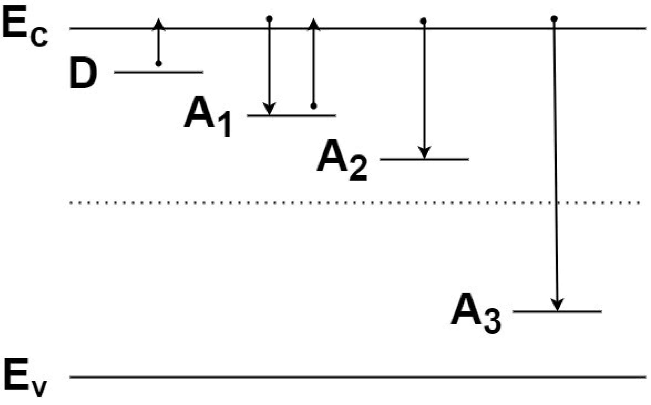
15]. Within the framework of the problem under consideration, these levels can be divided into three groups. Next, we will consider a simple model where each of these groups will be presented by one most characteristic level (
Figure 1):
1. Shallow donor level D with Nd concentration that existed in the sample before irradiation. The concentration of this level does not depend on the radiation dose. An impurity nitrogen level with an ionization energy Ei = 0.1 eV is considered such a level. With a sufficiently large fluence Φ, this level will be almost completely depleted in the quasi-neutral region. In the space charge layer, the level is completely empty at any Φ.
2. Relatively shallow acceptor level A1 with a concentration of
NA1. Its characteristic relaxation time to the equilibrium value,
, is determined by the time of electron emission from the level to the
C-band
τe and the capture time
τc. Such a level will be filled in the quasi-neutral region and emptied in the space charge layer. It is expedient to choose the Z
1/2 level with the ionization energy
Ei = 0.68 eV, as such a model level is in 4H-SiC [
5,
8]. The appearance of this level as a result of irradiation will reduce the electron concentration in the conduction band
n, determined from the current–voltage characteristics. However, as will be shown below, during
C–V measurements, this level will be completely empty and not affect the decrease in the
Nd −
Na value.
3. The A2 level is located in the upper half of the band gap, but its ionization energy (
Ec −
EA2) is quite high (>1 eV), so that during the characteristic time of measuring the
C–V characteristics, the ionization of electrons from this level can be neglected. It is expedient to choose the E
6/7 level with the ionization energy
Ei ~ 1.5 eV, as such a model level in 4H-SiC [
5,
8].
4. Level A3 is located in the lower half of the band gap, and its ionization energy is even higher. The total concentration of very deep levels will be denoted as NA = NA2 + NA3. These levels will decrease both the n value and the Nd − Na value.
Due to the large difference in the ionization energy of the levels under consideration, the concentration of electron
nj, supplied to the conduction band from each level, can be considered with good accuracy independent of the filling of all other levels. Then (see, for example, [
16]):
where
Nc is the density of states in the conduction band,
(here,
is the ionization energy of the corresponding level), and
g is the degeneracy factor of the corresponding level. In calculations, the
g was taken to be equal to unity (
g = 1).
At low radiation doses (Nd ≥ NA1 + NA), we took the total electron concentration n in the conduction band as the sum n1 + n2, where n1 and n2 are the concentrations of electrons delivered to the conduction band from levels D and A1, respectively, calculated by Formula (3).
When calculating the
n1 according to Formula (3), the
Nd −
Na will obviously be equal to
Nd −
Φ(a
A1 + a
NA), where a
A1 is the rate of center
A1 generation; a
NA is the total rate of all other acceptor levels’ generation. Note that the A1 level plays the role of an electron source in the
C-zone, especially at high temperatures [
17]. When calculating the value
nj = n2 according to (3), the
Nd −
Na will be equal to a
A1Φ.
At high radiation doses (Nd < NA1 + NA), the D level is completely empty. The residual conductivity of the base is due to the carrier’s ionization from level A1. Note that, in accordance with the adopted model, the probability of ionization from levels with higher ionization energies (A2 and A3 levels) is assumed to be zero.
In calculations, the rate of the center Z1/2 generation, determined from the analysis of DLTS spectra, was used.
Irradiation with 15 MeV energy protons was carried out in a portable MGTs-20 cyclotron. Irradiation with 0.9 MeV electrons was carried out on a resonant transformer accelerator. The electron beam’s current density was 12.5 µA cm−2. The pulse duration was 330 µs, and the pulse repetition rate was 490 Hz.
The carrier removal rates and generation rates of radiation defects used in the calculations are presented in
Table 1.
4. Results and Discussion
Let us consider the situation using an example of irradiation with protons and electrons of 4H-SiC Schottky diodes with a blocking voltage of 600 V. The initial concentration of donors in the base, that is, the concentration corresponding to the
D level,
Nd, is taken to be equal to 7 × 10
15 cm
−3 [
6]. The density of states,
Nc at room temperature in the 4H-SiC is
Nc ≈ 9 × 10
18 cm
−3. Electron mobility
μe is assumed to be independent of fluence
Φ and equal to 800 cm
2/Vs [
18].
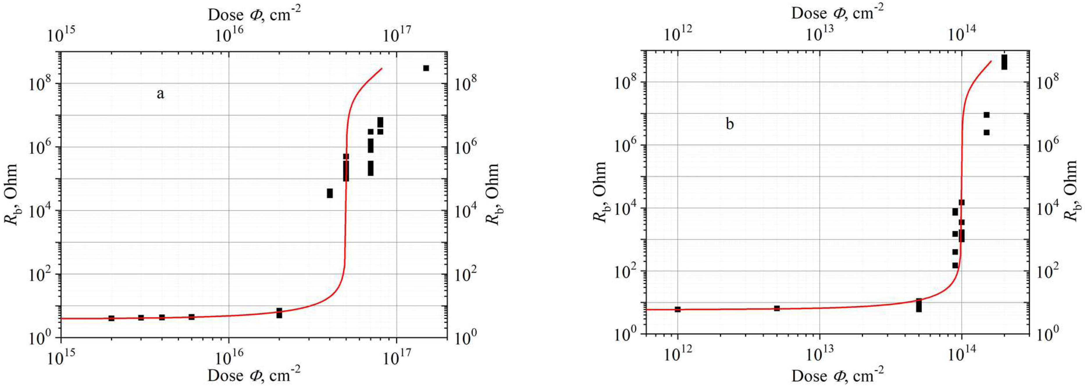
Figure 2 presents the experimental dependences of the diode base resistance
Rb = L/(enµS) on the doses with electron (
Figure 2a) and proton (
Figure 2b) irradiation [
11,
17]. Here,
e is the electron charge,
n is the electron concentration in the conduction band calculated in accordance with (3),
L = 10 μm, and
S = 6.75 × 10
−4 cm
−2 is the base length and diode area, respectively. These dependences are compared with the results of calculations in accordance with Equation (3).
Taking into account the fact that the change in the resistance
Rb was traced in
Figure 2 by eight orders of magnitude, the agreement between the experimental data and the calculations should be recognized as satisfactory. The obtained experimental results qualitatively agree with the data obtained in [
7] during irradiation of 4H-SiC structures with an initial electron concentration of 7.2 × 10
15 cm
−3 by electrons with an energy of 400 keV.
Two characteristic parts can be distinguished in
Figure 2.
At radiation doses of Φ ≤ 3 × 1016 cm−2 (electrons) and Φ ≤ 6 × 1013 cm−2 (protons), the resistance Rb increases relatively weakly (and practically linearly) with the radiation dose growth. This situation corresponds to the condition Nd ≥ NA1 + NA. Conductivity is due to electrons ionized from the shallow donor level D. In this case, the carrier removal rates calculated by Formulas (1) and (2) will be close.
At radiation doses
Φ ≥ 3 × 10
16 cm
−2 (electrons) and
Φ ≥ 6 × 10
13 cm
−2 (protons), there is a sharp increase in the base resistance with increasing
Φ. The shallow level D is almost completely compensated, and the residual conductivity is due to the generation of electrons to the conduction band from the A1 level. (In more accurate calculations, it should be taken into account that, in addition to the Z
1/2 level, which is presented in the model by the A1 level, electron irradiation also creates shallow levels with ionization energies of 0.25, 038, and 0.43 eV [
5]).
It should be emphasized that the type of dependences
Rb(
Φ), presented in
Figure 2a,b, is of a general nature and characteristic of all studied SiC Schottky diodes.
As mentioned above, when measuring the
C–V characteristics of reverse-biased Schottky diodes and p-n junctions, it is not the carrier concentration
n that is measured, but the
Nd −
Na value. In this case, when calculating the value of
n from the data of such measurements, it is assumed that all acceptor centers created by irradiation with a concentration of
Na remain negatively charged in the process of measuring the
C–V characteristics. However, when a reverse voltage is applied, the acceptor centers in the space charge region become empty (neutral), and do not contribute to the measured
Nd −
Na value. In this case, the characteristic time of electron emission
τe from the corresponding level after the application of the reverse voltage is of fundamental importance. This time can be estimated as [
19]:
where
σ is the capture cross-section,
νt is the electron thermal velocity, and
Nc is the density of states in the conduction band.
Taking for the Z
1/2 level (level A1 in
Figure 1) (
Ec −
Et) = 0.68 eV,
σ = 6 × 10
−14 cm
2,
vT ≈ 2 × 10
7 cm/s, and
Nc = 1.7 × 10
19 cm
−3 [5, 18), we get
τe ≈ 4 × 10
−2 s. For shallower levels with ionization energy 0.25, 038, and 0.43 eV [
5], the time of depletion will be even shorter. Such times are significantly shorter than the practical time of measurement of the
C–V characteristics. Thus, the value of
Nd −
Na obtained from
C–V measurements is not, strictly speaking, equal to the decrease in the electron concentration
n as a result of irradiation.
Note that for a deeper level A2 with an ionization energy
Ei ~ 1.5 eV (
Figure 1), identified with the E
6/7 level [
5,
8], the emission time will be ~5 × 10
12 s, which is many orders of magnitude greater than any practically acceptable time for measuring
C–V characteristics. Thus, the E
6/7 level and, of course, the levels lying in the lower half of the band gap will contribute to the measured
Nd −
Na value.
When estimating the n value from C–V measurements, a factor that makes it difficult to unambiguously interpret the experimental results is also a noticeable frequency dispersion of the capacitance of reverse-biased junctions in SiC structures.
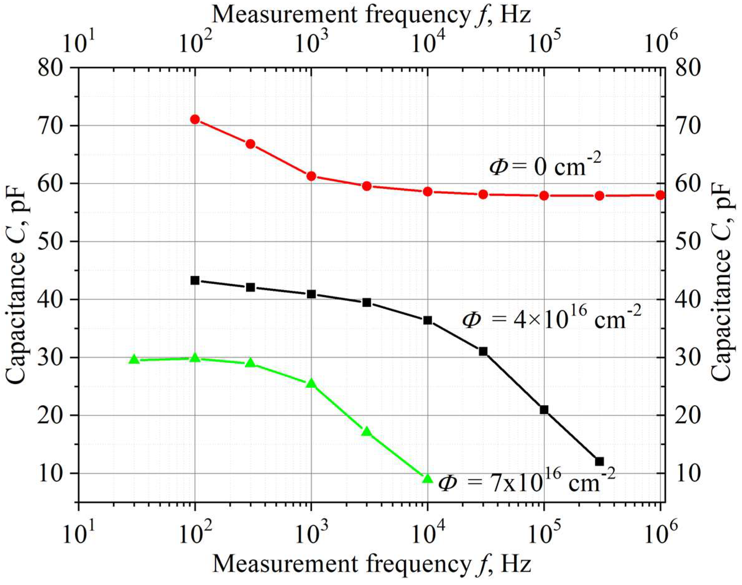
Figure 3 shows the frequency dependence of the capacitance of a reverse-biased high-voltage 4H-SiC Schottky diode (CPW4-1200S002B diode with 1200 V blocking voltage), measured in the Ref. [
11] over a wide frequency range.
As can be seen from
Figure 3, the frequency dispersion in a non-radiated diode is rather insignificant, and it can be neglected at frequencies
f ≥ 10 Hz. As the dose (fluence)
Φ increases, the dispersion increases greatly, reflecting the appearance of relatively shallow centers, rapidly emptying when reverse bias is applied. The frequency dependence of the capacitance is due to the fact that at high frequencies, the deep centers do not have time to ionize, and at low and high frequencies, they find themselves in different charge states, giving a different contribution to the value of the measured capacitance.
It is important to emphasize that when measuring the carrier concentration from
I–V characteristics, the directly measured value (base resistance
Rb) at an irradiation dose
Φ = 7 × 10
16 cm
−2 changes with respect to
Rb in a non-irradiated structure by ~5 orders of magnitude (
Figure 2a). With
C–V measurements, the capacitance under the same conditions only changes several times (
Figure 3). It is obvious that the determination of the concentration from the
I–V characteristics has an incomparably higher resolution.


