Article

Effect of Substrate Temperature on the Structural, Optical and Electrical Properties of DC Magnetron Sputtered VO2 Thin Films

1
Department of Electrical and Computer Engineering, University of Saskatchewan, Saskatoon, SK S7N 5A9, Canada
2
Cisco Systems Inc., 170 West Tasman Drive, San Jose, CA 95134, USA
3
Department of Mechanical Engineering, University of Saskatchewan, Saskatoon, SK S7N 5A9, Canada
*
Author to whom correspondence should be addressed.
Materials 2022, 15(21), 7849; https://doi.org/10.3390/ma15217849
Submission received: 17 September 2022 / Revised: 26 October 2022 / Accepted: 1 November 2022 / Published: 7 November 2022
(This article belongs to the Section Thin Films and Interfaces)

Abstract

:
This study focuses on the effect of the substrate temperature (TS) on the quality of VO2 thin films prepared by DC magnetron sputtering. TS was varied from 350 to 600 °C and the effects on the surface morphology, microstructure, optical and electrical properties of the films were investigated. The results show that TS below 500 °C favors the growth of V2O5 phase, whereas higher TS (≥500 °C) facilitates the formation of the VO2 phase. Optical characterization of the as-prepared VO2 films displayed a reduced optical transmittance ( T ˜ ) across the near-infrared region (NIR), reduced phase transition temperature (Tt), and broadened hysteresis width (ΔH) through the phase transition region. In addition, a decline of the luminous modulation ( Δ T ˜ lum ) and solar modulation ( Δ T ˜ sol ) efficiencies of the as-prepared films have been determined. Furthermore, compared with the high-quality films reported previously, the electrical conductivity (σ) as a function of temperature (T) reveals reduced conductivity contrast (Δσ) between the insulating and metallic phases of the VO2 films, which was of the order of 2. These outcomes indicated the presence of defects and unrelaxed lattice strain in the films. Further, the comparison of present results with those in the literature from similar works show that the preparation of high-quality films at TS lower than 650 °C presents significant challenges.

1. Introduction

Vanadium dioxide (VO2) has been widely studied for applications such as optical switches, sensors, smart windows, and optical memory devices [1,2,3,4]. Currently, potential applications can also be found in neuromorphic computing materials and metamaterials [5,6,7,8]. The primary reason for its importance in electronics, photonics and optical switching applications is the fast metal-to-insulator phase transition (MIT) between the semiconductor and metallic phases. During the MIT, the VO2 crystal undergoes an abrupt phase transformation from high temperature tetragonal phase to a low temperature monoclinic phase at around 68 °C [9]. Up to now, a variety of deposition methods (i.e., magnetron sputtering, pulsed laser deposition, chemical vapor deposition, electron beam evaporation etc.) have been employed to prepare VO2 thin films [10,11,12,13,14,15]. Regardless of the method, high growth temperatures (450–800 °C) are employed to assure its stoichiometry [16,17,18,19], which is crucial in the synthesis of VO2 thin films that display a sharp phase transition. However, instrumentation that delivers high substrate temperatures (TS) is costly and not industry-friendly [20]. For this reason, there have been numerous efforts to bring the TS down to more practical temperatures [21,22,23,24,25,26,27]. A few studies have already reported the fabrication of the VO2 thin films at low TS (down to around 300 °C) by applying a buffer layer such as ZnO, AZO, TiO2, SnO2 or VO [21,22,23]. Other pronounced efforts typically include substrate biasing, applying high power pulse, and post-annealing [24,25,26,27]. In order to reduce the TS, a clear understanding of the effect of the synthesis (substrate) temperature on the stoichiometry, structure and phase transition properties is critical. Some previous works have already revealed the effects of TS on the microstructure, stress state, and transition temperatures of VO2 thin films [16,28,29,30,31]. Nevertheless, these works are not comprehensive and do not necessarily signify a clear relation of the underlying mechanism related to physical changes due to the TS.
In our earlier works [17,32], we have reported the preparation of stoichiometric, near-epitaxial VO2 thin films at TS of 650 °C by DC reactive magnetron sputtering, where the films showed highly discernable optical and electrical phase transition properties (i.e., high optical transmittance ( Δ T ˜ ) and electrical conductivity (Δσ) contrasts, sharp transitions and near-zero optical transmission in the metallic phase). We have also investigated the effect of substrate biasing on the quality of VO2 thin films [33]. In the present work, we have undertaken the deposition of VO2 films at TS varying from 350 to 600 °C and examined the effects on the microstructure, surface morphology, roughness, optical and electrical phase transition properties. We compared these results with the films deposited at 650 °C in our previous works [17,32]. In addition, we extracted and analyzed the Δ T ˜ along with the luminous ( Δ T ˜ lum ) and solar ( Δ T ˜ sol ) optical modulation efficiencies. Furthermore, we estimated the electrical bandgap of the films and compared the results with those of high-quality VO2 thin films prepared at 650 °C reported previously [32]. Additionally, we compared our results with other works that studied the effect of TS on the properties of VO2 thin films.

2. Materials and Methods

Single crystal p-Si (100) and r-cut sapphire were used as substrates for the thin film preparation. Prior to the deposition, the substrates were ultrasonically cleaned in ethanol and dried in air. After the cleaning process, the substrates were placed in a sputtering chamber. DC reactive magnetron sputtering was utilized to prepare VO2 thin films. For this purpose, a high-purity vanadium target (99.95%, Plasmionique, Inc., Varennes, QC, Canada) was used. During every deposition, stable argon (Ar) and oxygen (O2) flow with constant rates of 100 sccm and 1.3 sccm were maintained, respectively. The selected Ar and O2 flow rates facilitate the growth of pure VO2 films using the above-mentioned deposition process which has been also reported in Ref. [17]. All depositions were performed under a constant pressure of 1.3 Pa for a duration of 2 h. The thin films were prepared at six different TS values. The deposition conditions for each TS are summarized in Table 1.
After deposition, the structural properties of the as-prepared thin films were examined at room temperature using Raman spectroscopy (Renishaw Invia Reflex Raman Microscope, Wharton-under-Edge, UK), scanning electron microscopy (Hitachi HT-7700 SEM, Tokyo, Japan), and X-ray diffractometry (Rigaku Ultima IV XRD, Tokyo, Japan). The average crystalline grain size was estimated using ImageJ (a software program developed by NIH, Bethesda, MD, USA [34]) on SEM images. Surface profilometry was used to examine the surface roughness of the films using a profilometer (Zygo OMP-0592, Middlefield, CT, USA). The optical transmittance spectrum was measured using a Lambda 900 UV-Vis-NIR Perkin-Elmer spectrophotometer (Waltham, MA, USA) in the wavelength (λ) range of 300–2500 nm. During the optical measurements, VO2-film/substrate sample was mounted on a purpose-built sample heating platform connected to a DC power supply (similar to the one in Ref. [32]). An Omega ® CN-16Pt-330 PID temperature controller (La Chaux-de-Fonds, Switzerland) was used to control the sample holder temperature and monitor the sample temperature during the heating and cooling processes. The temperature (T) dependence of the optical transmittance ( T ˜ ) measurements were conducted at a heating rate of ~0.5 °C/min. The T-dependence of the conductivity (σ) of the as-prepared films on sapphire substrates were carried out by depositing gold (Au) contacts at room temperature with the size of (1 mm × 2 mm) using a radio frequency (RF) sputtering system. These measurements were carried out in a cryostat where the samples were placed on a copper (Cu) block which was connected to a DC power supply. The supply was used to heat the block. The temperature of the samples was measured by the use of a thermocouple which was mounted in close proximity to the sample. During these measurements, the heating of the sample was specifically kept at a low rate (~0.5 °C/min) to prevent a lag between the temperature reading and the actual temperature of the sample.

3. Results

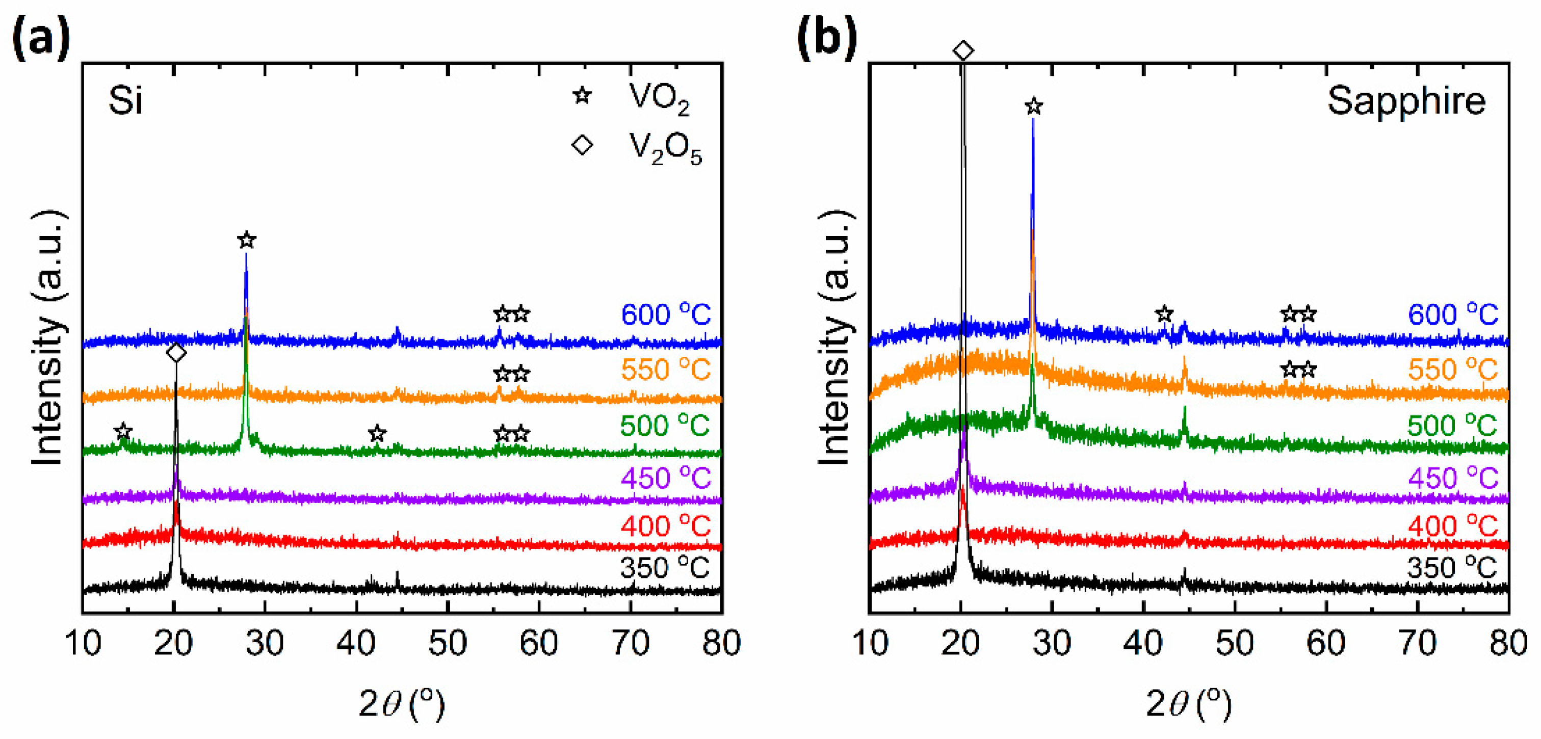
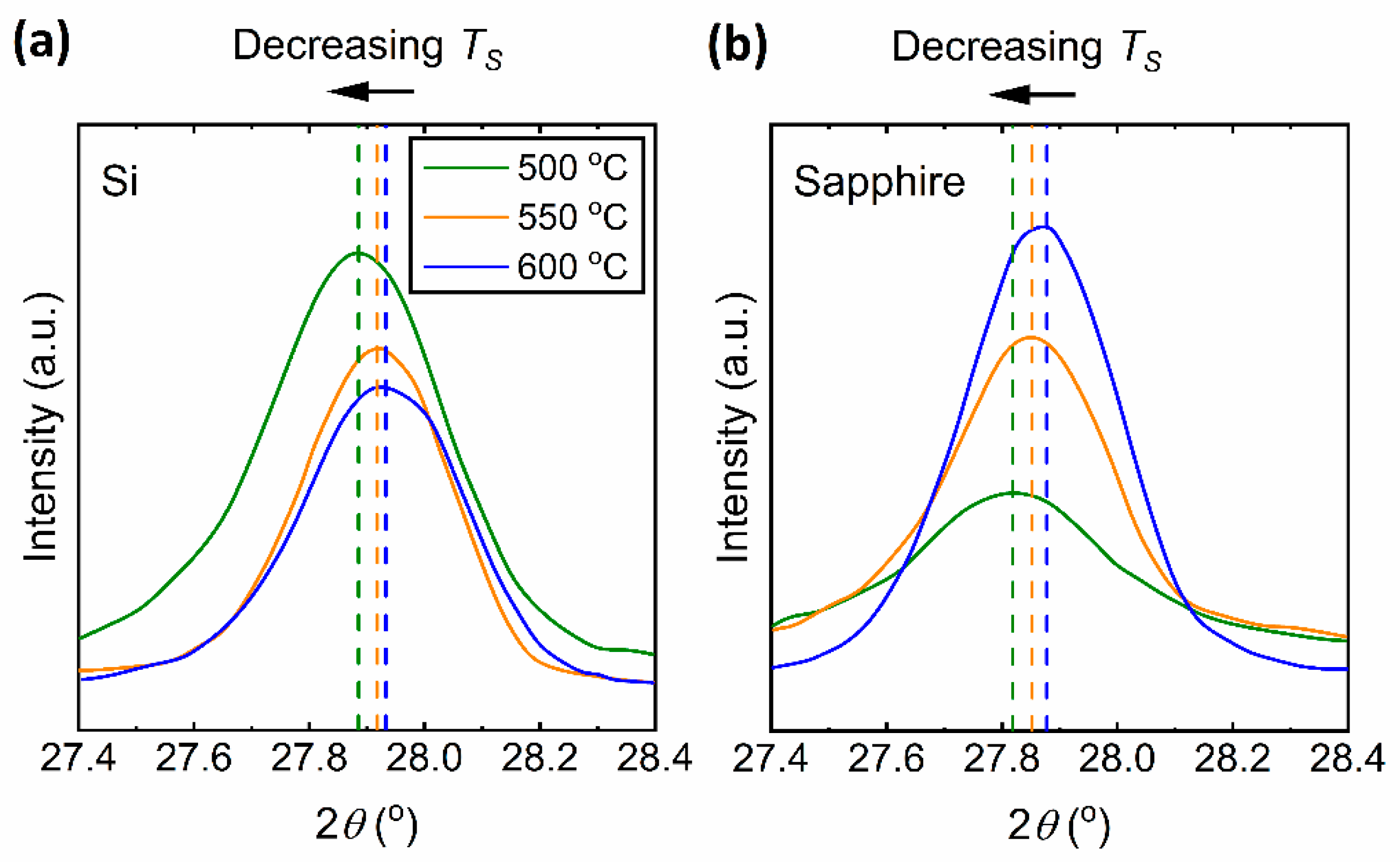
3.1. Microstructural Characterization by Raman Spectroscopy and XRD

The microstructural characterization of the vanadium oxide thin films prepared at different TS was carried out using Raman spectroscopy and x-ray diffraction (XRD) for which the results can be found in Figure 1 and Figure 2, respectively. These figures show that the pure monoclinic VO2 phase is achieved only for samples deposited at TS = 500 °C and higher temperatures. In Figure 1, the Raman peaks at 144, 193, 223, 260, 308, 334, 389, 497 and 613 cm−1 represent the pure monoclinic phase of VO2 [15]. In Figure 2, the diffraction peaks at 2θ = 28°, 56°, and 58° correspond to the (011), (220), and (022) of pure monoclinic phase of VO2 [35]. For TS = 450 °C, the Raman peaks of pure VO2 are not observed in Figure 1 and a small diffraction peak at 2θ = 20° appears in Figure 2, which corresponds to the (001) peak of V2O5. As the TS is further decreased down to 350 °C, the (001) peak of V2O5 dominates the XRD spectrum as can be seen in Figure 2a,b. The Raman peaks at 145, 195, 284, 303, 405, 483, 528, 701, and 996 cm−1 in Figure 1a,b, signify the presence of V2O5 phase to be the dominant in the thin film [15] below a TS of 450 °C. It can be seen that both Raman and XRD peaks of V2O5 become the strongest when the TS reaches 350 °C. It is worth mentioning that the sharp Raman peak around 520 cm−1 for the film deposited TS = 350 °C on a Si substrate arises from the Si substrate itself and is absent in films deposited on sapphire substrates.

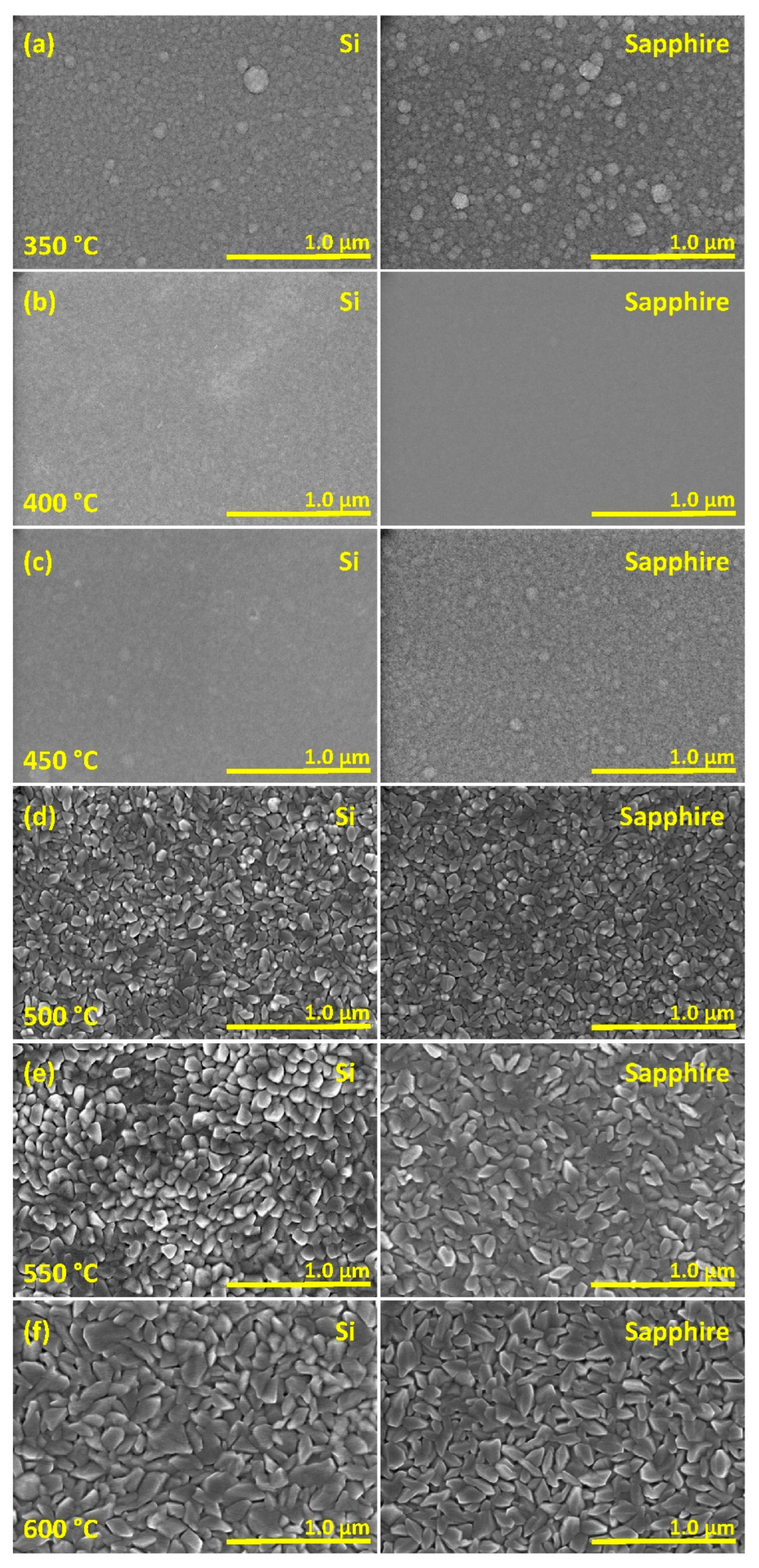
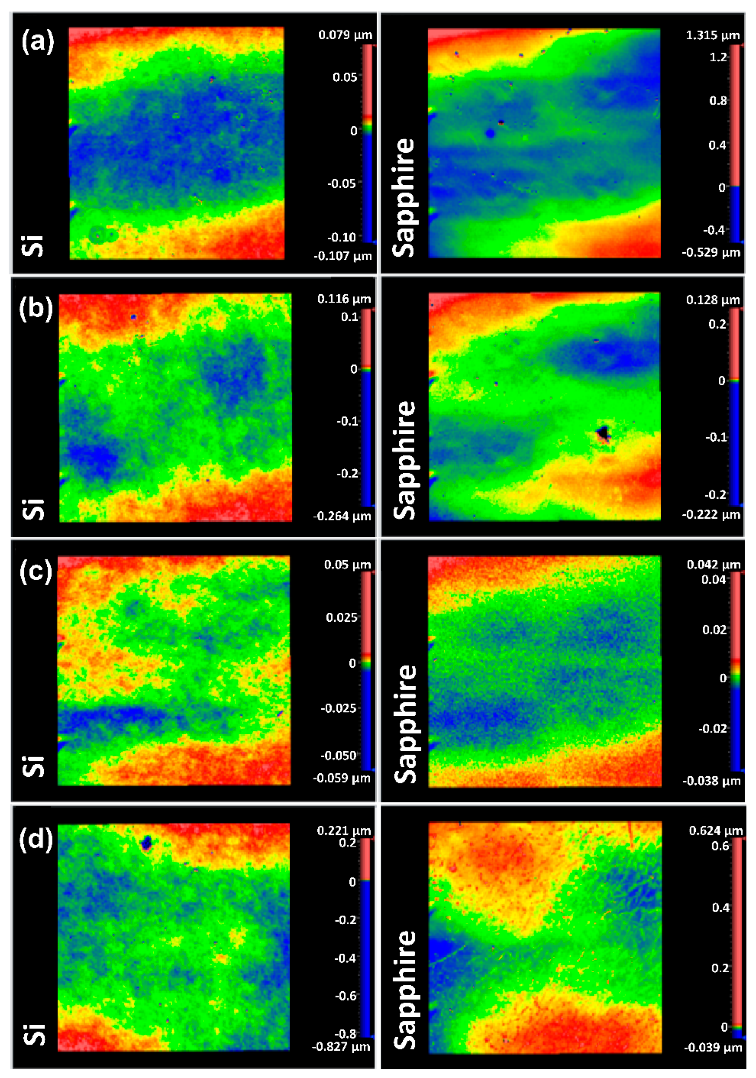
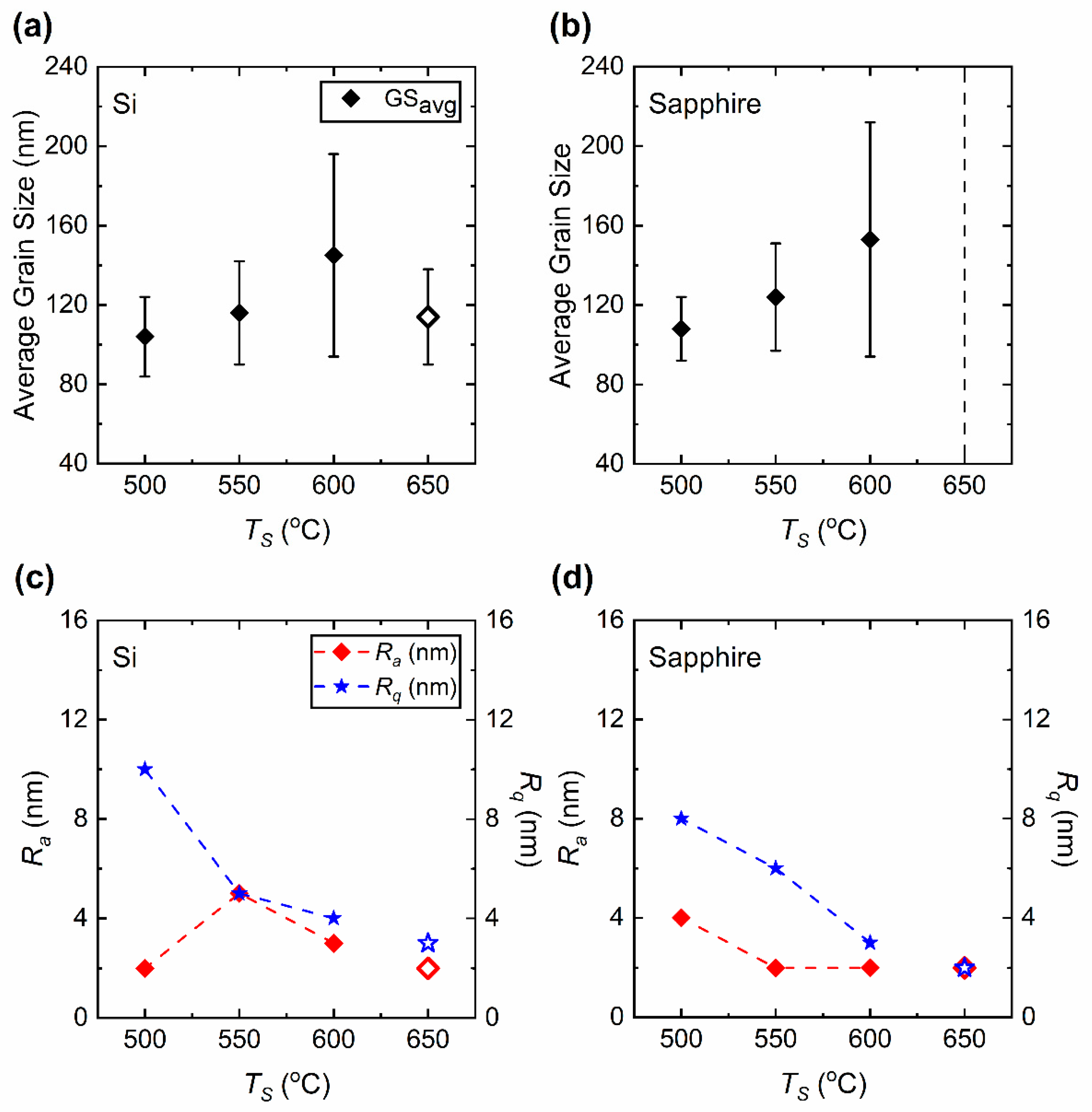
3.2. Surface Morphology and Roughness Characterization by SEM and Profilometry

Figure 3 presents the SEM surface images of the as-prepared VO2 thin films. It can be observed that the TS affects the surface morphology of the thin films. As observed from (a) to (b) to (c) the films show a misoriented crystalline structure with grain sizes ranging between around 100 and 150 nm. The substrate temperatures of 450 and 400 °C produce V2O5 nanostructured films with smooth surfaces. When the TS is lowered to 350 °C the V2O5 grains become clearly discernable in the films. Surface profilometry shows that TS also affects the surface roughness of VO2 films. Figure 4 shows the surface profile images of the VO2 films deposited at various TS-values. These images are taken at a surface area of approximately 0.6 × 0.6 mm2 of each film. Roughness measurements show that the root-mean-square (Rq) roughness of films on both Si and sapphire substrates increases as TS is lowered. The maximum Rq measured was obtained for VO2 films deposited at 500 °C, with 10 nm for films on Si and 8 nm for films on sapphire substrates. The minimum Rq is measured for films deposited at 600 °C as 4 nm on Si and 3 nm on sapphire substrates. Yet, these films show increased roughness compared to the films prepared at 650 °C [17]. The Rq is measured as 3 nm on Si and 2 nm on sapphire substrates for films prepared at 650 °C. These, in fact, manifest properties associated with high-quality VO2 films as investigated previously [36]. Nevertheless, the average roughness (Ra) does not exhibit a strong variation with respect to TS, in contrast to the clear trend exhibited by Rq. Table 2 and Figure 5 present the average grain size (GSavg), Ra and Rq of the VO2 thin films prepared on Si and sapphire substrates. The grain size in the films on sapphire substrates decreases from 153 nm to 108 nm as TS is lowered from 600 to 500 °C. Indeed, near-epitaxial growth on sapphire films has been reported in the literature [37]. On the other hand, the grain size of the films prepared on Si substrates, within experimental uncertainties, does not exhibit any compelling dependence on TS, even though there is seemingly a maximum average grain size at TS = 600 °C. Films on Si substrates prepared at 600 °C show grains with largely varying size (large standard deviation) and orientation. Even though the grain size is reduced for films prepared at TS = 550 and 500 °C the misorientation of grains is still evident. The thickness of the VO2 films prepared at TS = 600, 550 and 500 °C are measured by using cross-section SEM images as 210 ± 8, 230 ± 14, and 289 ± 15 nm, respectively.

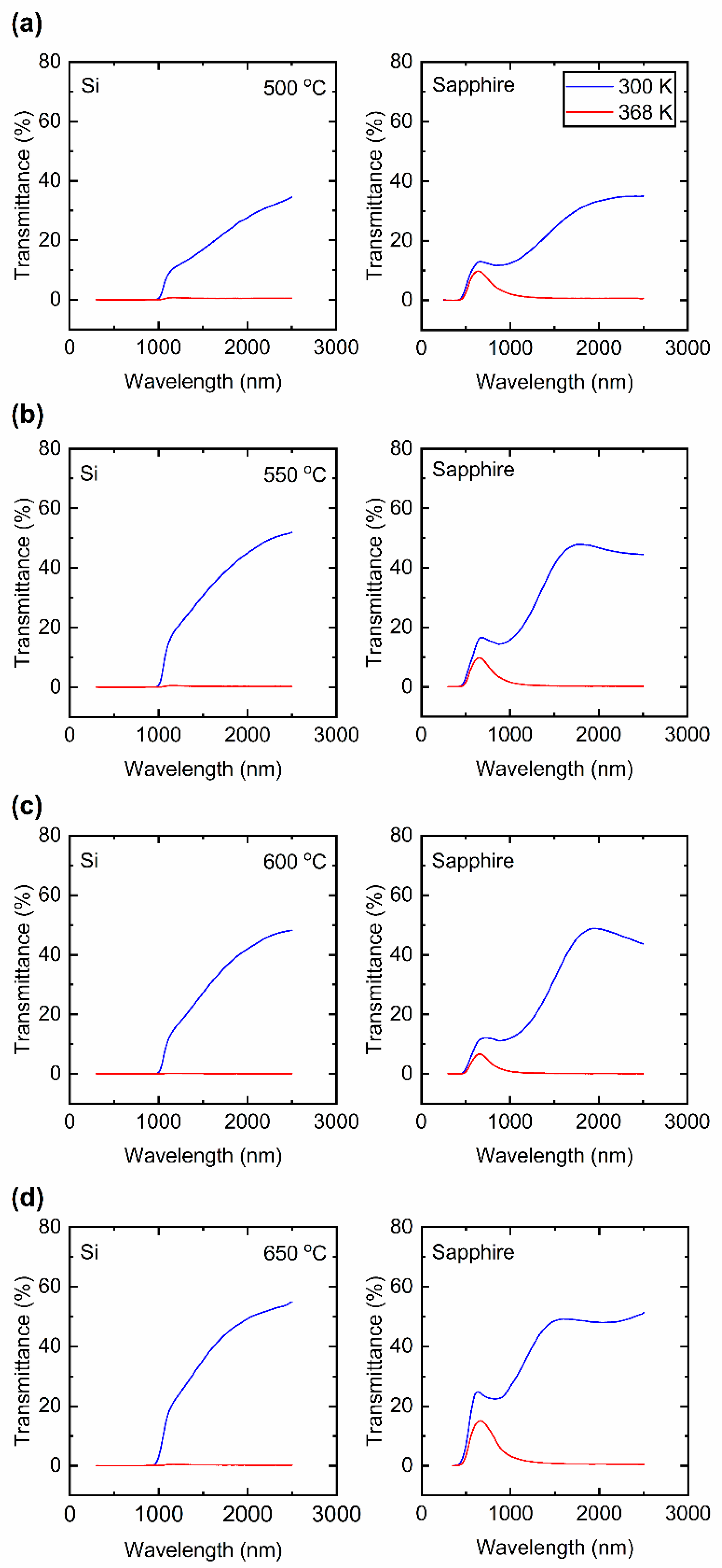
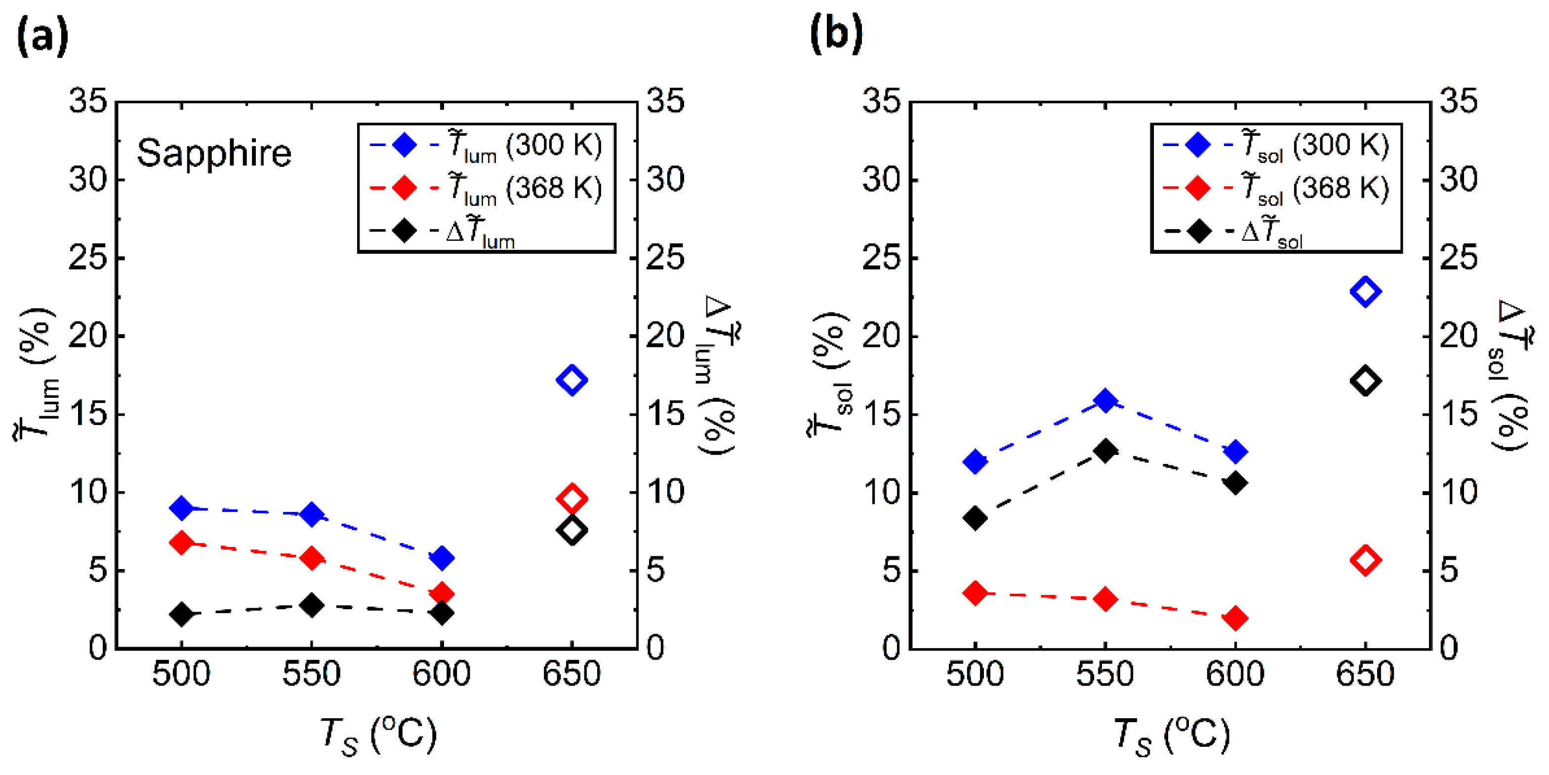
3.3. Optical Characterization by Spectrophotometry

To understand the effect of TS on the structural VO2 phase transition properties, the optical transmission ( T ˜ ) spectrum of VO2 thin films was measured at 300 K (27 °C) (in the insulating phase) and at 368 K (95 °C) (in the metallic phase) in a wavelength range between 300 and 2500 nm. Figure 6 presents the T ˜ spectra of these VO2 thin films. In practical terms, no notable difference can be found in the trend of the T ˜ spectra for samples prepared at TS = 600 and 550 °C. In Figure 6a, for the film prepared at TS = 500 °C, T ˜ 2500 nm is observed to be the lowest among other examined films, which is around 34% in the insulating phase. In Figure 6b,c the T ˜ of films deposited at TS = 550 and 600 °C on sapphire are observed to be very close. The drop of the T ˜ for films prepared at 500 °C can be related to the increased defects and the inferior crystal quality of VO2 thin films, which can be clearly observed in Figure 3d. At 368 K, all the VO2 films on both Si and sapphire substrates transition into a near-zero transmittance in the metallic phase. Table 3 presents the details of T ˜ values at 300 K and 368 K along with the optical transmittance contrast ( Δ T ˜ ) of the as-prepared VO2 films obtained at NIR wavelengths of 1500, 2000 and 2500 nm. Δ T ˜ is defined as the difference in the optical transmittance of the insulating and metallic phases.
Figure 7a gives the temperature dependence of T ˜ 2500 nm of the VO2 thin films prepared at various TS-values. Figure 7b–e show the d T ˜ / d T vs. T plots which give the critical temperatures (TIMT and TMIT) and sharpness (full width at half maximum, FWHM) of the IM and MI phase transitions. It is important to emphasize that the narrow and sharp hysteresis of IM and MI transitions in VO2 films deposited at 650 °C on sapphire substrate in Ref. [17] is not observed in the thin films deposited at TS = 600 °C and below. The hysteresis width (ΔH) of the films deposited on both Si and sapphire substrates become broader as the TS is lowered. The broadening appears to be about 14–16 K for films on Si and 13–21 K for films on sapphire.
Figure 8 presents the comparison of phase transition properties obtained at λ = 2500 nm. In Figure 8a the insulator-to-metal (TIMT), metal-to-insulator (TMIT) and the phase transition (Tt) temperatures are presented. The Tt is calculated as the mean of the TIMT and TMIT and is given in Equation (1) below:
T t = T IMT + T MIT 2
By definition, Tt depends on the hysteresis width (ΔH). It is observed that the critical temperatures on silicon substrates are relatively the same as TS is lowered from 650 [17] to 550 °C, but eventually decrease sharply for films prepared at 500 °C. For films on Si, as the Tt stays approximately constant for TS = 650, 600 and 550 °C at about 340 K but falls to 320 K for TS = 500 °C. On the other hand, the Tt of the films on sapphire appear to be lower compared to that for the film prepared at 650 °C in Ref. [17], displaying the lowest Tt around 322 K at 500 °C. There is no clear dependence of Tt on TS for films prepared on sapphire substrates. This change in Tt indicates increased defects in the VO2 films. In addition, the change may be attributed to the spatial variation of local TIMT and TMIT due to increased number of coexisting metallic and insulating phases within the volume of the films as pointed out elsewhere [38]. Figure 8b presents the ΔH and the full width half maximum (FWHM) of the IM and MI transitions of the as-prepared VO2 thin films. The increasing FWHM can be interpreted as the degrading sharpness of the phase transitions. Figure 8c introduces the comparison of transmittance contrast ( Δ T ˜ ) of the as-prepared films at λ = 1500, 2000, and 2500 nm which are commonly considered in NIR applications [39,40,41,42,43]. At lower TS, the ΔH becomes broader. The luminous (visible) and solar transmission characteristics of the as-prepared VO2 films deposited on sapphire substrates are also analyzed. The luminous transmittance ( T ˜ lum ), solar transmittance ( T ˜ sol ), the luminous modulation ( Δ T ˜ lum ) and solar modulation ( Δ T ˜ sol ) efficiencies are commonly considered properties for smart window applications [44,45,46,47,48,49,50]. T ˜ lum measures the amount of visible light passing through a semi-transparent material. T ˜ sol is considered as an index that characterizes the transmission of sunlight within the visible and near-infrared spectrum. T ˜ lum and T ˜ sol can be determined from Equation (2) below:
T ˜ lum , sol = φ lum , sol ( λ ) T ˜ ( λ ) d λ φ lum , sol ( λ ) d λ
T ˜ lum is obtained for a wavelength range between 380 and 780 nm and T ˜ sol is obtained for wavelengths between 300 and 2500 nm. φ lum ( λ ) is the spectral sensitivity of the light adapted human eye [51], φ sol ( λ ) is the solar irradiance spectrum for air mass of 1.5 (37° sunlight above the horizon of earth) [52], and T ˜ ( λ ) is acquired from the transmittance spectrum of the as-prepared films. Δ T ˜ lum and Δ T ˜ sol are calculated from the Equation (3) given below:
Δ T ˜ lum ,   sol = T ˜ lum ,   sol ( 300   K ) T ˜ lum ,   sol ( 368   K )
The results of the calculations of T ˜ lum , sol and Δ T ˜ lum , sol values are summarized in Table 4. Figure 9 gives the distribution of the data presented in Table 4. In Figure 9a, T ˜ lum values obtained for VO2 thin films prepared at TS = 500, 550 and 600 °C in the insulating phase (300 K) appear to be smaller from that obtained for films prepared at TS = 650 °C. The T ˜ lum values in the metallic phase (368 K) show a similar characteristic. Since the difference between T ˜ lum values obtained at 300 and 368 K is not large due to the high optical transmittance between 450 and 700 nm, the Δ T ˜ lum values are small. Figure 9b presents T ˜ sol and Δ T ˜ sol values of the as-prepared VO2 films which are also lower than those obtained for the film prepared at 650 °C [17]. However, the T ˜ sol values at 368 K are indeed much lower compared to the ones at 300 K, due to the near-zero transmission in the NIR region integrated in Equation (2). This large difference between the T ˜ sol values at 300 and 368 K is reflected on the large values of Δ T ˜ sol .

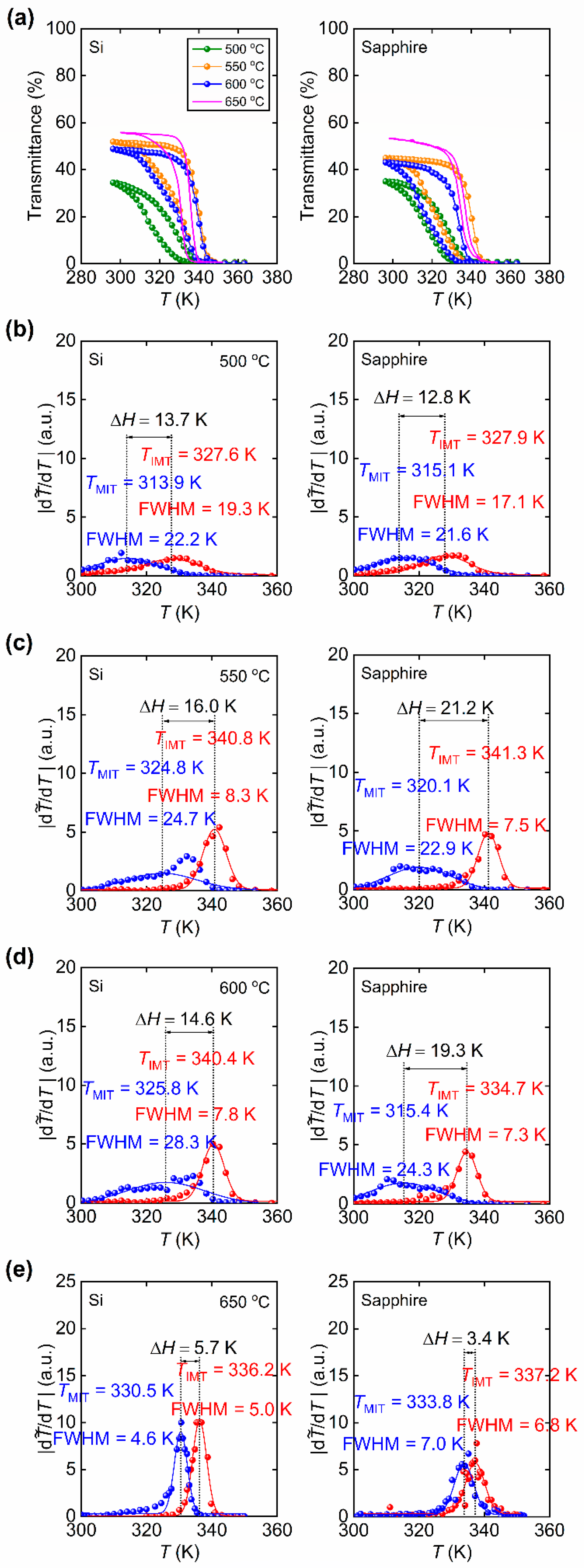
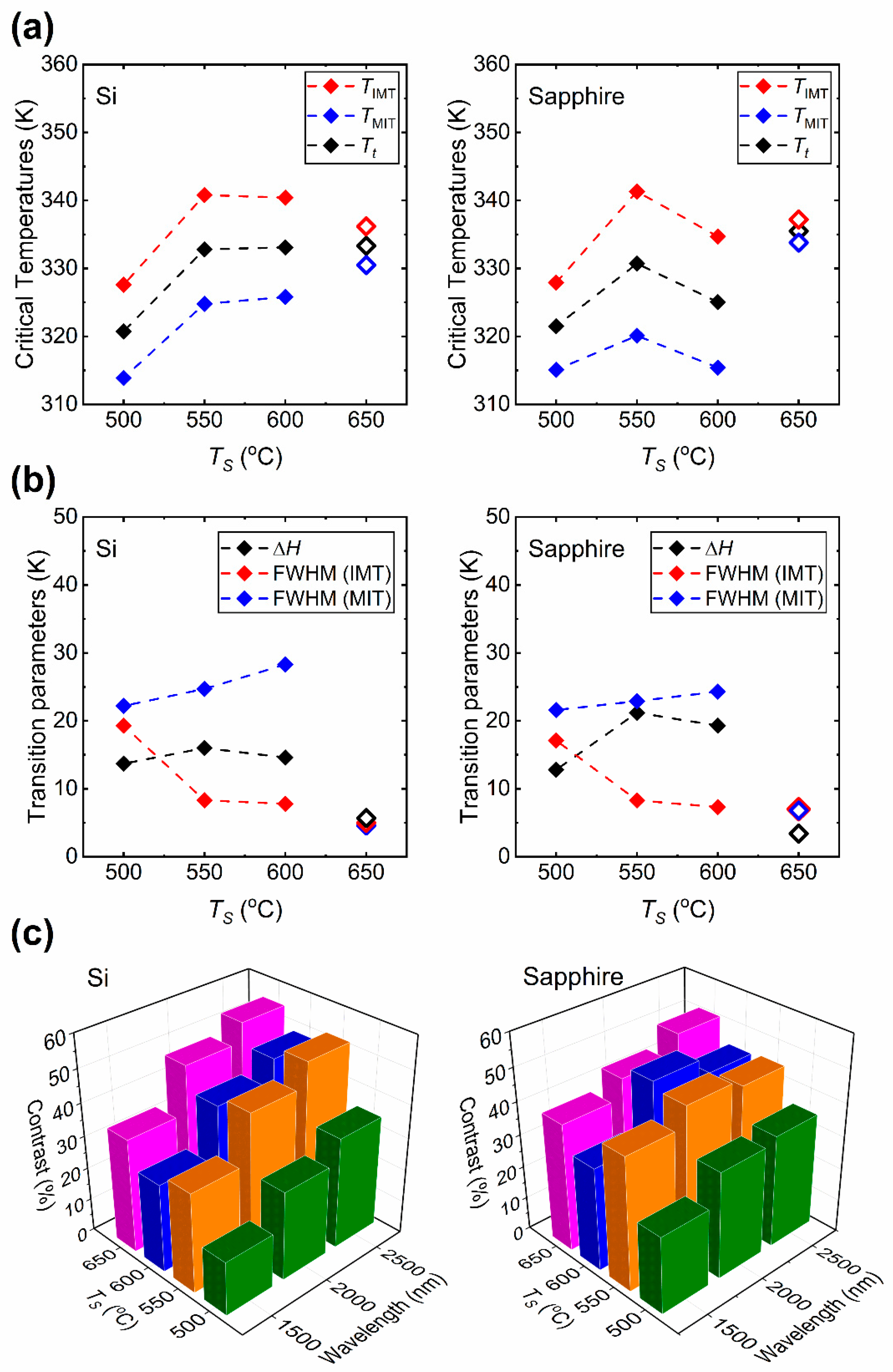
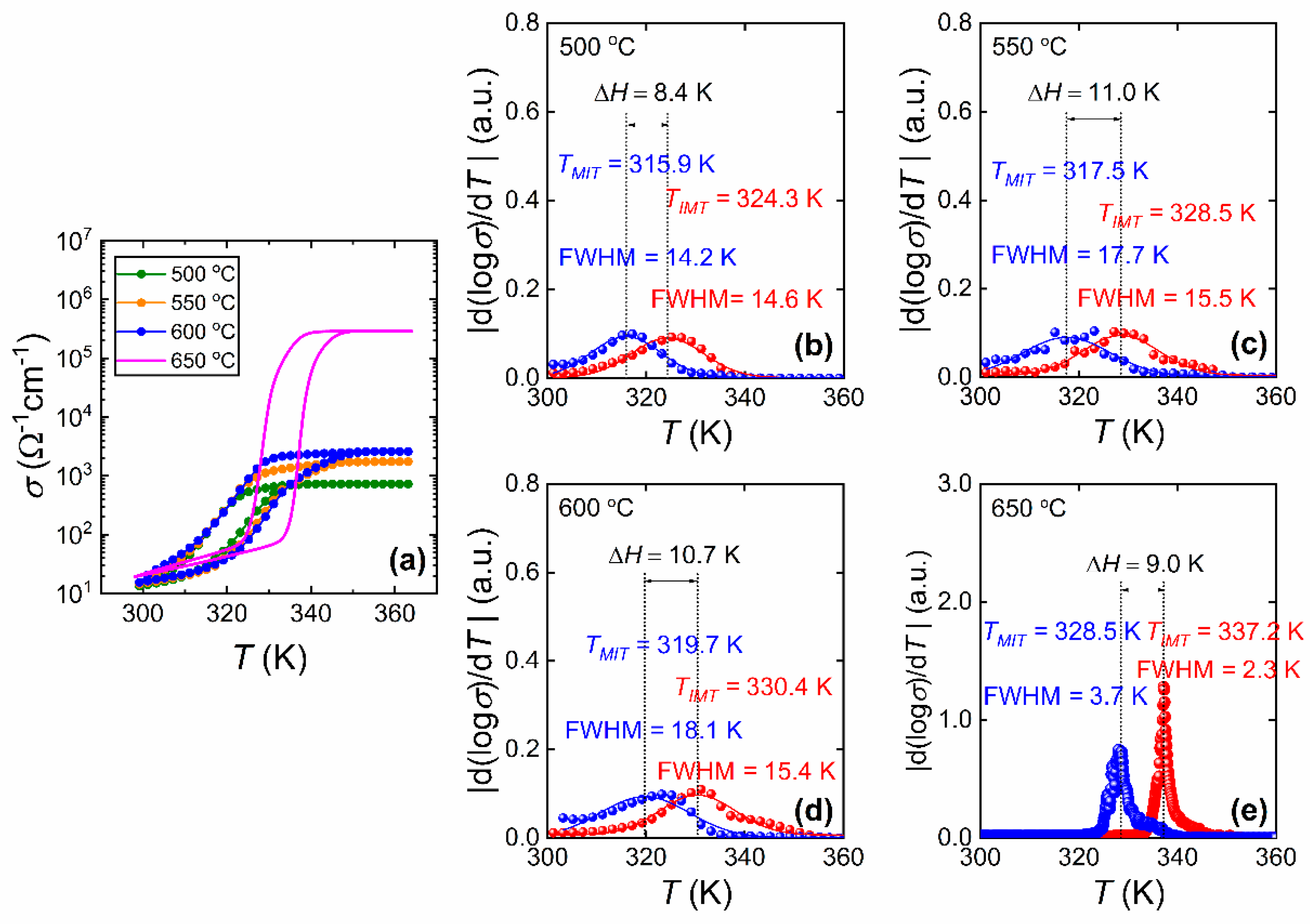
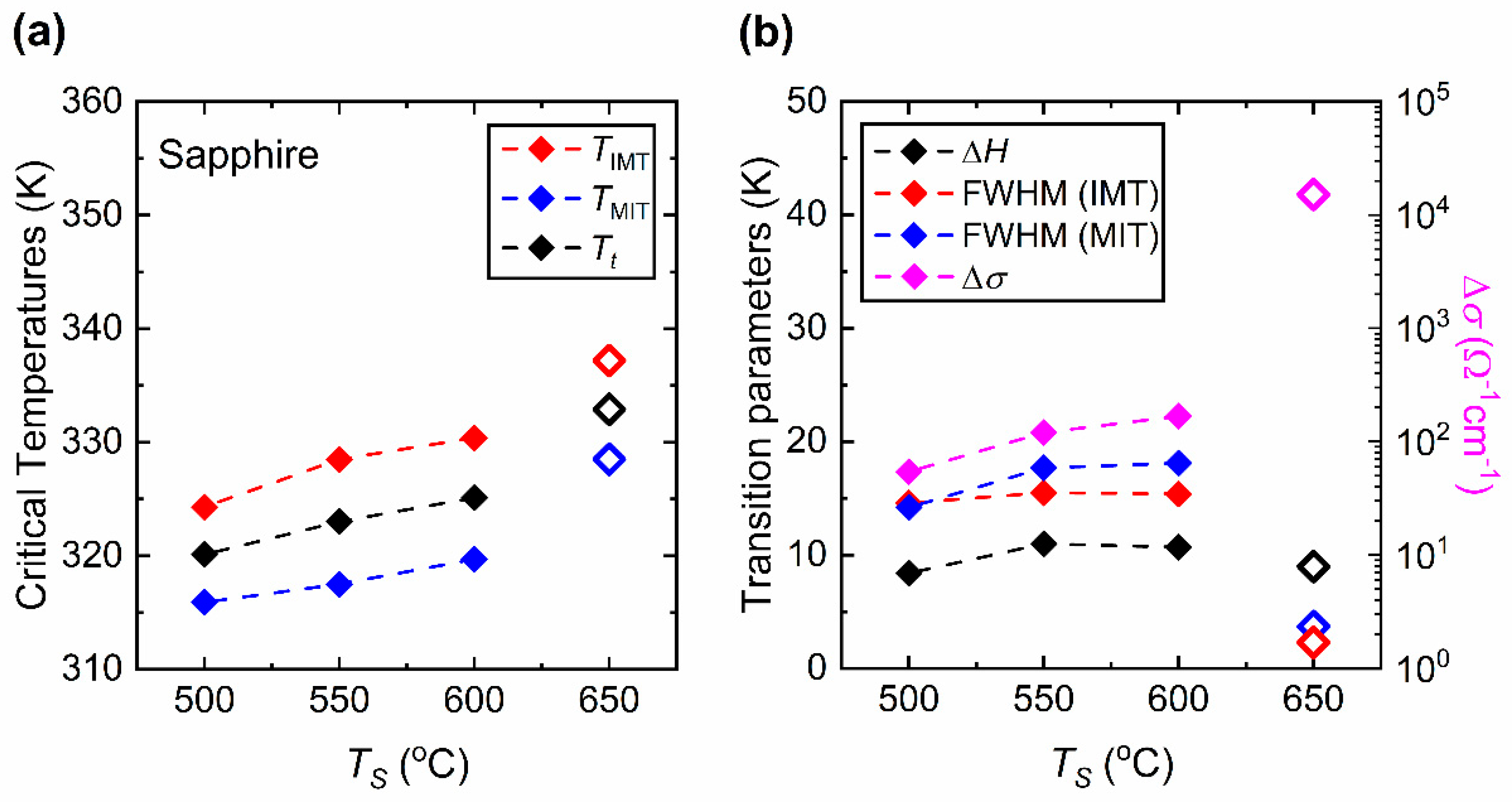
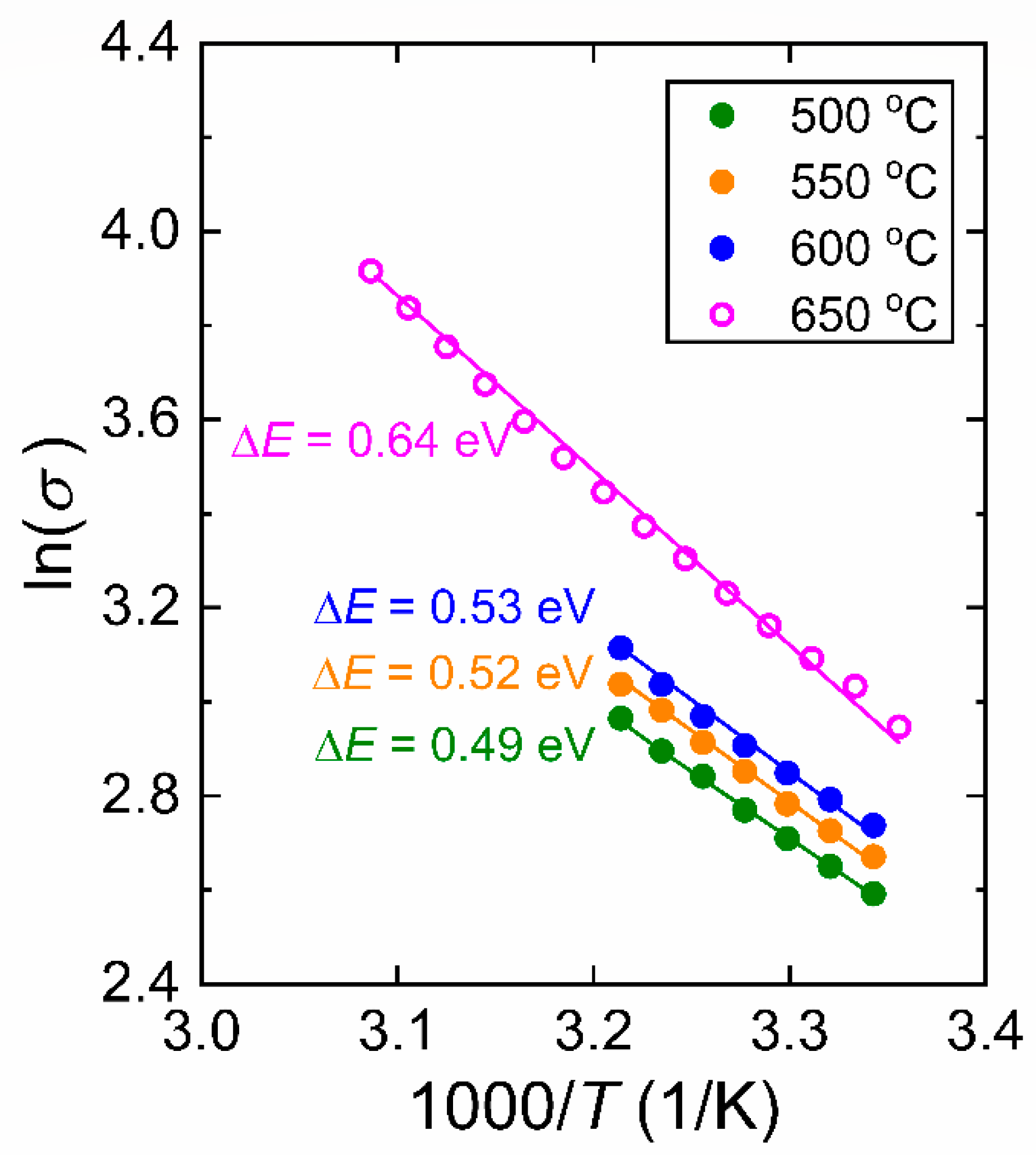
3.4. Electrical MIT Characterization

Figure 10a shows the temperature (T) dependence of the electrical conductivity (σ) of the VO2 films prepared at TS = 500, 550, 600 and 650 [32] °C, and their phase transition properties. The critical temperatures TIMT, TMIT and the sharpness (FWHM) are obtained from the d(log(σ))/dT vs. T. plots as shown in Figure 10b–e. Here, it can be seen that there is only a slight broadening of the ΔH. On the other hand, the electrical phase transition properties of VO2 thin films studied in this work show a prominent difference compared to the film prepared at TS = 650 °C in Ref. [32]. The difference between the hysteresis properties of the samples is due to the difference in the nature of electrical and structural (observed optically) MIT [33,53]. Figure 11 gives the critical temperatures and phase transition parameters of VO2 films deposited on sapphire substrates obtained in σ vs. T measurements. As it is clear from the Figure 11a, the transition temperatures (TIMT, TMIT and Tt) drop with decreasing TS. In Figure 11b, the ΔH does not seem to be greatly affected from TS. As the TS is lowered from 650 to 550 °C, the ΔH broadens from 9 to 11 K, respectively. However, for TS = 500 °C, the ΔH drops to 8.4 K which shows narrower ΔH compared to the other VO2 films. On the other hand, the effect of TS appears to be prominent in the sharpness of both IM and MI transitions and the conductivity contrast (Δσ). The FWHM of the films prepared between 500 and 600 °C are larger compared with those of the film prepared at 650 °C in both IM and MI transitions. The increase of FWHM, or loss of sharpness, in films between 500 and 600 °C indicates degradation of the abrupt phase transition. In addition, compared to the high-quality VO2 films prepared at 650 °C (Ref. [32]), the Δσ of the films prepared at TS = 600 °C and below displays a substantial drop from the order of 4 to 2.

4. Discussion

We begin our discussion by considering the structural investigation of VO2 thin films. The results presented in Figure 1, Figure 2, Figure 3 and Figure 4 clearly show that the TS has a considerable effect on the film structure, including both the crystallinity and surface roughness. For TS between 600 and 500 °C, both the XRD diffractograms and the Raman spectra show VO2 peaks, which disappear for TS ≤ 450 °C. From this observation, it can be understood that higher TS (≥500 °C) facilitates the formation of the VO2 phase, whereas lower temperature growth favors the formation of the V2O5 phase as can be referred to in Table 1. Since the V2O5 phase appears at lower TS and the root mean square roughness (Rq) increases with lower TS, one may argue that there may be a correlation between the two observations. Nonetheless, we do not have any further experimental evidence to validate the latter. Yet, it is apparent from Figure 3 that low TS leads to a polycrystalline structure of misoriented grains with dissimilar geometries. Thus, not only the smaller grain size but also the increased defects in the films at low TS (e.g., 500 °C) may explain the drop in the T ˜ spectrum. Secondly, the drop in the transition temperature (Tt) can be related to the significance of unrelaxed lattice strain [54,55]. The degradation of the crystalline quality can be seen in the worsening of the phase transition properties given in Figure 7. Moreover, considering the electrical characterization, the degradation of contrast in the conductivity between the insulator and metallic phases (Δσ) may be a result of the reduction of the current path due to increased oxygen vacancies and surface roughness [56]. We also examined the conductivity activation energy of the as-prepared VO2 films. The Arrhenius plot of ln(σ) vs. 1000/T is presented in Figure 12 where it is apparent that the conductivity (σ) of VO2 is thermally activated. We can represent the thermally activated behavior by,
σ = σ o exp Δ E 2 k B T
where ΔE = Eg if we assume the sample is intrinsic. Equation (4) yields ΔE of the VO2 films as 0.53 ± 0.02, 0.52 ± 0.01 and 0.49 ± 0.01 eV corresponding to prepared at TS = 600, 550 and 500 °C, respectively. The thermally activated conductivity can arise either from intrinsic conductivity (thermal generation across the bandgap) with ΔE = Eg as in Equation (4) or from the ionization of defects or impurities in the film, in which case ΔE is not the bandgap but the magnitude of the energy difference between the transport band and the defect or impurity level. The ΔE values appear to be lower than that of high-quality VO2 films, which is 0.64 ± 0.01 eV from Ref. [36]. The ΔE values seem to follow a similar trend to that of Δσ with respect to TS in Figure 11b. The drop in Δσ and the apparent narrowing of ΔE may too be related to the increased density of grain boundaries and defects of oxygen vacancies due to low TS which is pointed out in Ref. [57]. In addition, Figure 13 presents the shifting of the amplified XRD peak of VO2 (011) at ~28° to a lower angle as TS decreases. This signifies an enlarged lattice parameter of VO2 due to defects and lattice strain, which is also suggested in Ref. [56]. It is worth comparing ΔE = 0.49–0.64 eV for these VO2 films with the indirect (smallest) optical bandgap reported for VO2 films deposited at 650 °C, which is 0.52 eV [17]. The work in Ref. [33] puts the optical bandgap between in the range 0.55–0.60 eV; again ΔE is very close to these values.
Finally, we compare our results with other works [21,28,30,57] in which the effect of TS on the phase transition properties of VO2 thin films have been studied. These studies have employed RF reactive inverted cylindrical magnetron sputtering [21], RF magnetron sputtering [28], inductively coupled plasma (ICP)-assisted sputtering [30], and pulsed-laser deposition (PLD) [57] for thin film preparation. We also consider selected works [26,36] which have reported the production of high-quality VO2 thin films at low substrate temperatures. Figure 14 presents the phase transition properties of VO2 thin films obtained by means of optical transmittance ( T ˜ ) and electrical conductivity (σ) measurements. Figure 14a,b show the comparison of the Tt and ΔH characteristics of the films on sapphire substrates from the present work with the films prepared in Refs. [21,30]. It should be noted that the optical transmittance has been measured at different wavelengths. VO2 films reported in Ref. [26] were prepared at TS = 200 °C by reactive magnetron sputtering with a post-deposition annealing treatment at 300 °C, and the transition properties were obtained at λ = 2000 nm. The present work has used λ = 2500 nm, whereas λ = 1450 nm for Ref. [21] and 1100 nm for Ref. [30] were used. In Figure 14a, the films in Ref. [21] have a constant Tt around 340 K, whereas the Tt of films in Ref. [30] decreases from Ts = 600 to 500 °C and stays constant around 343 K until Ts = 450 °C. In contrast, the Tt of the VO2 films on sapphire substrates presented in this work drops down to 323 K as the TS is lowered to 500 °C. As can be observed in Figure 14b, reducing the TS has a significant impact on the ΔH of the films prepared in the present work which can be related to the polycrystallinity as well as increased compressive and tensile strain in the films [28,32]. Figure 14c,d present the comparison of electrical phase transition properties obtained from Refs. [28,57]. Moreover, VO2 films reported in Ref. [36] were prepared by molecular beam epitaxy (MBE) at TS = 350 °C. In Figure 14c, the Tt of the films of Ref. [28] increases from a low TS = 450 to 550 °C and then drops at high TS = 700 and 720 °C. On the contrary, in Figure 14d, the ΔH values appear to be relatively unaffected by TS, and they seem to be mostly constant around 5.5 K, only films prepared at 450 °C have a large ΔH around 10 K. The Tt values obtained from Ref. [57] are constant around 343 K. In addition, the ΔH drops with decreasing TS from 13 K and 5 K. However, if the phase transition sharpness and Δσ are taken into consideration, these films in Refs. [28,57] do not display attributes associated with high-quality films with decreasing TS. Overall, according to these comparisons, the preparation of high-quality VO2 films at low temperatures appear to be a challenge even though different deposition techniques and deposition parameters are applied. The degradation of the film properties may essentially rise from loss of crystalline quality, the degradation of stoichiometry (e.g., if there is an interface film between VO2 and the substrate) and the presence of defects and lattice strain that arise from film-substrate mismatch.

5. Conclusions

The effect of substrate temperature (TS) on the structural, optical and electrical properties of VO2 thin films during DC magnetron sputtering have been investigated. The results showed that the TS plays a crucial role on the microstructure and hence the optical and electrical phase transition properties of the VO2 films. It is found that TS below 500 °C favors the growth of the V2O5 phase where TS of 500 °C and higher facilitate the growth of stoichiometric VO2 films. The lowering of TS from 600 to 500 °C have shown reduced optical transmittance ( T ˜ ) and modulation efficiencies, broadened hysteresis width (ΔH), and decreased transition temperature, which suggests the presence of defects and unrelaxed lattice strain in the films. The comparison of the present results with those published on similar VO2 samples, where the effect of TS has been examined, indicates significant challenges remain in the fabrication of high-quality VO2 films below a TS of 650 °C.

Author Contributions

Conceptualization and formulation of ideas, C.Z., O.G., S.K., S.-J.W. and Q.Y.; methodology, C.Z., O.G. and S.K.; investigation, C.Z. and O.G.; writing—original draft preparation, C.Z. and O.G.; writing—review and editing, O.G. and S.K., overall supervision, Q.Y. and S.K. All authors have read and agreed to the published version of the manuscript.

Funding

This research was funded jointly by NSERC (CRD) and Cisco University Research Program Fund (through Silicon Valley Community Foundation CG#602057).

Data Availability Statement

Data is available from the corresponding author upon reasonable request.

Acknowledgments

The authors want to thank Cisco Systems, and the Natural Science and Engineering Research Council of Canada (NSERC) for their financial support. The authors also acknowledge Saskatchewan Structural Sciences Centre (SSSC) for providing facilities and assistance to conduct the Raman and XRD tests.

Conflicts of Interest

The authors declare no conflict of interest.

References

  1. Zhou, H.; Li, J.; Xin, Y.; Sun, G.; Bao, S.; Jin, P. Optical and electrical switching properties of VO2 thin film on MgF2 (111) substrate. Ceram. Int. 2016, 42, 7655–7663. [Google Scholar] [CrossRef]
  2. Simo, A.; Kaviyarasu, K.; Mwakikunga, B.; Madjoe, R.; Gibaud, A.; Maaza, M. Phase transition study in strongly correlated VO2 based sensing systems. J. Electron Spectrosc. Relat. Phenom. 2017, 216, 23–32. [Google Scholar] [CrossRef]
  3. Malarde, D.; Powell, M.J.; Quesada-Cabrera, R.; Wilson, R.L.; Carmalt, C.J.; Sankar, G.; Parkin, I.P.; Palgrave, R.G. Optimized atmosphere-pressure Chemical Vapor Deposition thermochromic VO2 thin films for intelligent window applications. ACS Omega 2017, 2, 1040–1046. [Google Scholar] [CrossRef] [Green Version]
  4. Coy, H.; Cabrera, R.; Sepulveda, N.; Fernandez, F.E. Optoelectronic and all-optical multiple memory states in vanadium dioxide. J. Appl. Phys. 2010, 108, 113115. [Google Scholar] [CrossRef] [Green Version]
  5. Hong, X.; Loy, D.J.; Dananjaya, P.A.; Tan, F.; Ng, C.; Lew, W. Oxide-based RRAM materials for neuromorphic computing. J. Mater. Sci. 2018, 53, 8720–8746. [Google Scholar] [CrossRef]
  6. Yang, Z.; Ko, C.; Ramanathan, S. Oxide Electronics Utilizing Ultrafast Metal-Insulator Transitions. Annu. Rev. Mater. Res. 2011, 41, 337–367. [Google Scholar] [CrossRef]
  7. Jeong, J.; Jung, Y.; Qu, Z.; Cui, B.; Khanda, A.; Sharma, A.; Parkin, S.S.P.; Poon, J.K.S. VO2 electro-optic memory and oscillator for neuromorphic computing. In Proceedings of the 2020 Conference on Lasers and Electro-Optics (CLEO), San Jose, CA, USA, 10–15 May 2020. paper STh3R.2. [Google Scholar] [CrossRef]
  8. Liu, H.; Lu, J.; Wang, X.R. Metamaterials based on the phase transition of VO2. Nanotechnology 2018, 29, 024002. [Google Scholar] [CrossRef]
  9. Goodenough, J.B. The two components of the crystallographic transition in VO2. J. Solid State Chem. 1971, 3, 490–500. [Google Scholar] [CrossRef]
  10. Hajlaoui, T.; Emond, N.; Quirouette, C.; Drogoff, B.L.; Margot, J.; Chaker, M. Metal–insulator transition temperature of boron-doped VO2 thin films grown by reactive pulsed laser deposition. Scr. Mater. 2020, 177, 32–37. [Google Scholar] [CrossRef]
  11. Rajeswaran, B.; Umarji, A.M. Defect engineering of VO2 thin films synthesized by Chemical Vapor Deposition. Mater. Chem. Phys. 2020, 245, 122230. [Google Scholar] [CrossRef]
  12. Leroy, J.; Bessaudou, A.; Cosset, F.; Crunteanu, A. Structural, electrical and optical properties of thermochromic VO2 thin films obtained by reactive electron beam evaporation. Thin Solid Films 2012, 520, 4823–4825. [Google Scholar] [CrossRef]
  13. Gagaoudakis, E.; Aperathitis, E.; Michail, G.; Panagopoulou, M.; Katerinopoulou, D.; Binas, V.; Raptis, Y.S.; Kiriakidis, G. Low-temperature rf sputtered VO2 thin films as thermochromic coatings for smart glazing systems. Sol. Energy 2018, 165, 115–121. [Google Scholar] [CrossRef]
  14. Li, M.; Magdassi, S.; Gao, Y.; Long, Y. Hydrothermal Synthesis of VO2 Polymorphs: Advantages, Challenges and Prospects for the Application of Energy Efficient Smart Windows. Small 2017, 13, 1701147. [Google Scholar] [CrossRef] [PubMed]
  15. Zhang, C.Z.; Yang, Q.; Koughia, C.; Ye, F.; Sanayei, M.; Wen, S.J.; Kasap, S. Characterization of vanadium oxide thin films with different stoichiometry using Raman spectroscopy. Thin Solid Films 2016, 620, 64–69. [Google Scholar] [CrossRef]
  16. Lafane, S.; Abdelli-Messaci, S.; Kechouane, M.; Malek, S.; Guedouar, B.; Lappalainen, J.; Nemraoui, O.; Kerdj, T. Direct growth of VO2 nanoplatelets on glass and silicon by pulsed laser deposition through substrate temperature control. Thin Solid Films 2017, 632, 119–127. [Google Scholar] [CrossRef]
  17. Zhang, C.Z.; Koughia, C.; Güneş, O.; Luo, J.; Hossain, N.; Li, Y.S.; Cui, X.; Wen, S.J.; Wong, R.; Yang, Q.; et al. Synthesis, structure and optical properties of high-quality VO2 thin films grown on silicon, quartz and sapphire substrates by high temperature magnetron sputtering: Properties through the transition temperature. J. Alloys Compd. 2020, 848, 156323. [Google Scholar] [CrossRef]
  18. Umar, Z.A.; Ahmed, N.; Ahmed, R.; Arshad, M.; Anwar-Ul-Haq, M.; Hussain, T.; Baig, M.A. Substrate temperature effects on the structural, compositional, and electrical properties of VO2 thin films deposited by pulsed laser deposition, Surf. Interface Anal. 2018, 50, 297–303. [Google Scholar] [CrossRef]
  19. Diallo, A.; Ndiaye, N.M.; Ngom, B.D.; Khamlich, S.; Talla, K.; Ndiaye, S.; Manyala, N.; Nemraoui, O.; Madjoe, R.; Beye, A.C.; et al. Effect of substrate temperature on the structure and the metal insulator transition in pulsed laser deposed VO2\films on soda lime glass. J. Opt. 2015, 44, 36–44. [Google Scholar] [CrossRef] [Green Version]
  20. Houska, J. Design and reactive magnetron sputtering of thermochromic coatings. J. Appl. Phys. 2022, 31, 110901. [Google Scholar] [CrossRef]
  21. Sato, K.; Hoshino, H.; Mian, S.; Okimura, K. Low-temperature growth of VO2 films on transparent ZnO/glass and Aldoped ZnO/glass and their optical transition properties. Thin Solid Films 2018, 651, 91–96. [Google Scholar] [CrossRef]
  22. Sun, G.; Cao, X.; Li, X.; Bao, S.; Li, N.; Liang, M.; Gloter, A.; Gu, H.; Jin, P. Low-temperature deposition of VO2 films with high crystalline degree by embedding multilayered structure. Sol. Energy Mater. Sol. Cells 2017, 161, 70–76. [Google Scholar] [CrossRef]
  23. Xiang, Z.; Wu, Z.; Ji, C.; Shi, Y.; Dai, J.; Huang, Z.; Xu, W.; Dong, X.; Wang, J.; Jiang, Y. Low temperature fabrication of high-performance VO2 film via embedding low vanadium buffer layer. Appl. Surf. Sci. 2020, 517, 146101. [Google Scholar] [CrossRef]
  24. Zhu, M.; Qi, H.; Li, C.; Wang, B.; Wang, H.; Guan, T.; Zhang, D. VO2 thin films with low phase transition temperature grown on ZnO/glass by applying substrate DC bias at low temperature of 250 °C. Appl. Surf. Sci. 2018, 453, 23–30. [Google Scholar] [CrossRef]
  25. Houska, J.; Kolenaty, D.; Vlcek, J.; Cerstvy, R. Properties of thermochromic VO2 films prepared by HiPIMS onto unbiased amorphous glass substrates at a low temperature of 300 °C. Thin Solid Films 2018, 660, 463–470. [Google Scholar] [CrossRef]
  26. Melnik, V.; Khatsevych, I.; Kladko, V.; Kuchuk, A.; Nikirin, V.; Romanyuk, B. Low-temperature method for thermochromic high ordered VO2 phase formation. Mater. Lett. 2012, 68, 215–217. [Google Scholar] [CrossRef]
  27. Guo, B.; Chen, L.; Shi, S.; Ishaq, A.; Wan, D.; Chen, Z.; Zhang, L.; Luo, H.; Gao, Y. Low temperature fabrication of thermochromic VO2 thin films by low-pressure chemical vapor deposition. RSC Adv. 2017, 7, 10798–10805. [Google Scholar] [CrossRef] [Green Version]
  28. Lee, D.; Yang, D.; Kim, H.; Kim, J.; Song, S.; Choi, K.S.; Bae, J.S.; Lee, J.; Lee, J.; Lee, Y.; et al. Deposi-tion-Temperature-Mediated Selective Phase Transition Mechanism of VO2 Films. J. Phys. Chem. C 2020, 124, 17282–17289. [Google Scholar] [CrossRef]
  29. McGee, R.; Goswami, A.; Khorshidi, B.; McGuire, K.; Schofield, K.; Thundat, T. Effect of process parameters on phase stability and metal-insulator transition of vanadium dioxide (VO2) thin films by pulsed laser deposition. Acta Mater. 2017, 137, 12–21. [Google Scholar] [CrossRef]
  30. Kana Kana, J.B.; Ndjaka, J.M.; Ngoma, B.D.; Fasasi, A.Y.; Nemraoui, O.; Nemutudi, R.; Knoesen, D.; Maaza, M. High substrate temperature induced anomalous phase transition temperature shift in sputtered VO2 thin films. Opt. Mater. 2010, 32, 739–742. [Google Scholar] [CrossRef]
  31. Kana Kana, J.B.; Ndjaka, J.M.; Ngom, B.D.; Manyala, N.; Nemraoui, O.; Fasasi, A.Y.; Nemutudi, R.; Gibaud, A.; Knoesen, D.; Maaza, M. Thermochromic nanocrystalline Au–VO2 composite thin films prepared by radiofrequency inverted cylindrical magne-tron sputtering. Thin Solid Films 2010, 518, 1641–1647. [Google Scholar] [CrossRef] [Green Version]
  32. Koughia, C.; Gunes, O.; Zhang, C.; Wen, S.J.; Wong, R.; Yang, Q.; Kasap, S.O. Topology of conductive clusters in sputtered high-quality VO2 thin films on the brink of percolation threshold during insulator-to-metal and metal-to-insulator transitions. J. Vac. Sci. Technol. A Vac. Surf. Films 2020, 38, 063401. [Google Scholar] [CrossRef]
  33. Zhang, C.; Gunes, O.; Li, Y.; Cui, X.; Mohammadtaheri, M.; Wen, S.J.; Yang, Q.; Kasap, S. The effect of substrate biasing during DC magnetron sputtering on the quality of VO2 thin films and their insulator–metal transition behavior. Materials 2019, 12, 2160. [Google Scholar] [CrossRef] [PubMed] [Green Version]
  34. Image Processing and Analysis in Java. Available online: https://imagej.nih.gov/ij/ (accessed on 14 September 2022).
  35. Majid, S.S.; Shukla, D.K.; Rahman, F.; Khan, S.; Gautam, K.; Ahad, A.; Francoual, S.; Choudhary, R.J.; Sathe, V.G.; Strempfer, J. Insulator-metal transitions in the T phase Cr-doped and M1 phase undoped VO2 thin films. Phys. Rev. B 2018, 98, 075152. [Google Scholar] [CrossRef]
  36. Zhang, H.T.; Zhang, L.; Mukherjee, D.; Zheng, Y.X.; Haislmaier, R.C.; Alem, N.; Engel-Herbert, R. Wafer-scale growth of VO2 thin films using a combinatorial approach. Nat. Commun. 2015, 6, 8475. [Google Scholar] [CrossRef] [Green Version]
  37. Creeden, J.A.; Madaras, S.E.; Beringer, D.B.; Beebe, M.R.; Novikova, I.; Lukaszew, R. Structural and photoelectric properties of epitaxially grown vanadium dioxide thin films on c-plane sapphire and titanium dioxide. Sci. Rep. 2019, 9, 9362. [Google Scholar] [CrossRef] [PubMed] [Green Version]
  38. Miyazaki, K.; Shibuya, K.; Suzuki, M.; Wado, H.; Sawa, A. Correlation between thermal hysteresis width and broadening of metal–insulator transition in Cr-and Nb-doped VO2 films. Jpn. J. Appl. Phys. 2014, 53, 071102. [Google Scholar] [CrossRef]
  39. Liang, J.; Li, P.; Zhou, L.; Guo, J.; Zhao, Y. Near-infrared tunable multiple broadband perfect absorber base on VO2 semi-shell arrays photonic microstructure and gold reflector. Mater. Res. Express 2018, 5, 015802. [Google Scholar] [CrossRef]
  40. Chu, X.; Xie, Q.; Zhang, X.; Guo, B.; Liao, J.; Zhao, X. Fabrication and Optical Characterization of VO2-Based Thin Films Deposited on Practical Float Glass by Magnetron Sputtering and Professional Annealing. Materials 2022, 15, 2990. [Google Scholar] [CrossRef]
  41. Zhang, D.-P.; Zhu, M.-D.; Liu, Y.; Yang, K.; Liang, G.-X.; Zheng, Z.-H.; Cai, X.-M.; Fan, P. High performance VO2 thin films growth by DC magnetron sputtering at low temperature for smart energy efficient window application. J. Alloys Compd. 2016, 659, 198–202. [Google Scholar] [CrossRef]
  42. Ko, B.; Badloe, T.; Kim, S.J.; Hong, S.H.; Rho, J. Employing vanadium dioxide nanoparticles for flexible metasurfaces with switchable absorption properties at near-infrared frequencies. J. Opt. 2020, 22, 114002. [Google Scholar] [CrossRef]
  43. Son, S.B.; Youn, J.W.; Kim, K.S.; Kim, D.U. Optical properties of periodic micropatterned VO2 thermochromic films prepared by thermal and intense pulsed light sintering. Mater. Des. 2019, 182, 107970. [Google Scholar] [CrossRef]
  44. Vu, T.D.; Liu, S.; Zeng, X.; Li, C.; Long, Y. High-power impulse magnetron sputtering deposition of high crystallinity vanadium dioxide for thermochromic smart windows applications. Ceram. Int. 2020, 46, 8145–8153. [Google Scholar] [CrossRef]
  45. Wang, S.; Wei, W.; Huang, T.; Yuan, M.; Yang, Y.; Yang, W.; Dai, N. Al-Doping-Induced VO2 (B) Phase in VO2 (M) Toward Smart Optical Thin Films with Modulated ΔTvis and ΔTc. Adv. Eng. Mater. 2019, 21, 1900947. [Google Scholar] [CrossRef]
  46. Ji, C.; Wu, Z.; Wu, X.; Wang, J.; Gou, J.; Huang, Z.; Zhou, H.; Yao, W.; Jiang, Y. Al-doped VO2 films as smart window coatings: Reduced phase transition temperature and improved thermochromic performance. Sol. Energy Mater. Sol. Cells 2018, 176, 174–180. [Google Scholar] [CrossRef]
  47. Zhao, X.; Hu, X.; Sun, J.; You, Q.; Xu, H.; Liu, W.; Sun, G.; Nie, Y.; Yao, W.; Jiang, X. VO2-based composite films with exemplary thermochromic and photochromic performance. J. Appl. Phys. 2020, 128, 185107. [Google Scholar] [CrossRef]
  48. Zhao, X.P.; Mofid, S.A.; Gao, T.; Tan, G.; Jelle, B.P.; Yin, X.B.; Yang, R.G. Durability-enhanced vanadium dioxide ther-mochromic film for smart windows. Mater. Today Phys. 2020, 13, 100205. [Google Scholar] [CrossRef]
  49. Cui, Y.; Ke, Y.; Liu, C.; Chen, Z.; Wang, N.; Zhang, L.; Zhou, Y.; Wang, S.; Gao, Y.; Long, Y. Thermochromic VO2 for energy-efficient smart windows. Joule 2018, 2, 1707–1746. [Google Scholar] [CrossRef] [Green Version]
  50. Li, B.; Tian, S.; Wang, Z.; Liu, B.; Gong, X.; Zhao, X. Thermochromic Ta Doped VO2 Films: Enhanced Luminous Transmittance, Significantly Depressed Phase Transition Temperature and Hysteresis Width. Appl. Surf. Sci. 2021, 568, 150959. [Google Scholar] [CrossRef]
  51. Hunt, R.W.G. The Reproduction of Colour, 6th ed.; Kriss, M.A., Ed.; John Wiley & Sons: West Sussex, UK, 2004; pp. 678–679. [Google Scholar]
  52. Reference Air Mass 1.5 Spectra. Available online: https://www.nrel.gov/grid/solar-resource/spectra-am1.5.html (accessed on 14 September 2022).
  53. Gunes, O.; Koughia, C.; Zhang, C.; Belev, G.; Wen, S.J.; Yang, Q.; Kasap, S.O. Self-heating-induced electrical and optical switching in high quality VO2 films controlled with current pulses. J. Mater. Sci. Mater. 2021, 32, 24285–24295. [Google Scholar] [CrossRef]
  54. Sang, J.; Zheng, T.; Xu, L.; Zhou, X.; Tian, S.; Sun, J.; Xu, X.; Wang, J.; Zhao, S.; Liu, Y. Modulating the metal-insulator transition in VO2/Al2O3 (001) thin films by grain size and lattice strain. J. Alloys Compd. 2021, 876, 160208. [Google Scholar] [CrossRef]
  55. Yang, T.H.; Aggarwal, R.; Gupta, A.; Zhou, H.; Narayan, R.J.; Narayan, J. Semiconductor-metal transition characteristics of VO2 thin films grown on c-and r-sapphire substrates. J. Appl. Phys. 2010, 107, 053514. [Google Scholar] [CrossRef]
  56. Yoon, J.; Park, C.; Park, S.; Mun, B.S.; Ju, H. Correlation between surface morphology and electrical properties of VO2 films grown by direct thermal oxidation method. Appl. Surf. Sci. 2015, 353, 1082–1086. [Google Scholar] [CrossRef]
  57. Kang, C.; Wei, Z.; Zhang, C.; Liang, S.; Geng, C.; Wu, J.; Liu, H.; Zong, H.; Li, M. Evolution of polymorph and photoelectric properties of VO2 thin films with substrate temperature. J. Alloys Compd. 2019, 803, 394–400. [Google Scholar] [CrossRef]
Figure 1. Raman spectra of VO2 and V2O5 thin films prepared at various substrate temperatures (TS) on (a) Si and (b) sapphire substrates. Note that the vertical axes are in arbitrary units (a.u.), so the relative magnitudes of the spectra cannot be compared.
Materials 15 07849 g001
Figure 2. XRD spectra of VO2 and V2O5 thin films prepared at various substrate temperatures (TS) on (a) Si and (b) sapphire substrates. Note that the vertical axes are in arbitrary units (a.u.).
Materials 15 07849 g002
Figure 3. Surface images of VO2 and V2O5 thin films prepared at various substrate temperatures (TS) (a) 350 °C, (b) 400 °C, (c) 450 °C, (d) 500 °C, (e) 550 °C, and (f) 600 °C obtained by SEM.
Materials 15 07849 g003
Figure 4. Surface profile images of VO2 thin films deposited on Si and sapphire substrates at (a) 500 °C, (b) 550 °C, (c) 600 °C and (d) 650 °C [17]. The roughness of the surface is indicated by color mapping, where the maximum (peak), median and minimum (depth) points on the surface are indicated in red, green and blue, respectively. The scale bars are used as a measure of the peaks and depths on the surface of the films.
Materials 15 07849 g004
Figure 5. Average grain size (GSavg) of VO2 thin films prepared on (a) Si and (b) sapphire substrates. In (b) the dashed vertical line is an asymptote that indicates the near-epitaxial almost flat surface of the film prepared at 650 °C [17]. (c,d) present the average (Ra) and root-mean-square (Rq) roughness of films prepared on Si and sapphire substrates, respectively. The dashed lines between the data points are guides to the eye. The data points shown in hollow symbols belong to the films prepared at 650 °C (prepared as described in Ref. [17] but not reported therein).
Materials 15 07849 g005
Figure 6. Optical transmittance ( T ˜ ) spectra of VO2 thin films deposited at (a) 500 °C, (b) 550 °C, and (c) 600 °C and (d) 650 °C [17] on Si and sapphire substrates at 300 K (insulating phase) and 368 K (metallic phase).
Materials 15 07849 g006
Figure 7. (a) Temperature dependence of optical transmittance ( T ˜ ) obtained at a light wavelength of λ = 2500 nm for VO2 thin films deposited at 500, 550, 600 and 650 °C [17]. The phase transition characteristics for heating and cooling cycles for films prepared at (b) 500 °C, (c) 550 °C, (d) 600 °C, and (e) 650 °C [17] on Si and sapphire substrates at 300 K (insulating phase) and 368 K (metallic phase).
Materials 15 07849 g007
Figure 8. (a) Critical temperatures (TIMT, TMIT and Tt) of the VO2 films on Si and sapphire prepared at various substrate temperatures (TS) obtained at a light wavelength of λ = 2500 nm. (b) Hysteresis (ΔH) and sharpness (FWHM) of the Gaussian curves obtained from d T ˜ / d T vs. T plots in Figure 7. In (a) and (b) the data points for films prepared at 650 °C [17] are shown in hollow symbols. (c) Comparison of optical transmittance contrast, Δ T ˜ = T ˜ ( 300   K ) T ˜ ( 368   K ) , obtained at NIR wavelengths λ = 1500 nm, 2000 nm and 2500 nm for films prepared at TS = 500 (olive), 550 (orange), 600 (navy) and 650 [17] (magenta) °C.
Materials 15 07849 g008
Figure 9. (a) Luminous transmittance ( T ˜ lum ) at 300 K and 368 K and luminous modulation efficiency ( Δ T ˜ lum ) obtained for films deposited at various substrates temperatures (TS). (b) Solar transmittance ( T ˜ sol ) at 300 K and 368 K and solar modulation efficiency ( Δ T ˜ sol ) obtained for films deposited at various substrates temperatures (TS). Data for the substrate temperature (TS) of 650 °C [17] are presented in hollow symbols.
Materials 15 07849 g009
Figure 10. Temperature (T) dependence of electrical conductivity (σ) of VO2 films prepared at various substrate temperatures (TS). (a) Comparison of T dependence of σ of films prepared at TS = 500 °C, 550 °C, 600 °C, and 650 °C [32]. The phase transition characteristics for heating and cooling cycles for films prepared at TS = (b) 500 °C, (c) 550 °C, (d) 600 °C and (e) 650 °C [32].
Materials 15 07849 g010
Figure 11. Electrical conductivity phase transition properties of VO2 films prepared on sapphire substrates at various substrate temperatures (TS). (a) Critical temperatures of the phase transition (TIMT, TMIT and Tt). (b) Phase transition parameters (ΔH, FWHM (IMT), and FWHM (MIT)) and the contrast of conductivity, Δσ = σ(368 K)/σ(300 K). The data points for the substrate temperature 650 °C are from Ref. [32] and displayed in hollow symbols.
Materials 15 07849 g011
Figure 12. Arrhenius plot of conductivity (σ) data obtained from VO2 films in their insulating phases. Data set for VO2 film prepared at 650 °C is extracted from the σ vs. T plot in Ref. [32].
Materials 15 07849 g012
Figure 13. X-ray diffraction of (011) planes of VO2 thin films deposited at TS = 500, 550, and 600 °C on (a) Si and (b) sapphire substrates.
Materials 15 07849 g013
Figure 14. Comparison of VO2 thin films deposited at various temperatures studied in different works. (a) Comparison of Tt obtained from optical (O-) switching measurements. (b) Hysteresis width (ΔH) of the films that are obtained from the temperature (T) dependence of optical transmittance ( T ˜ ). (c) Comparison of phase transition temperature (Tt) obtained from electrical (E-) switching. (d) Hysteresis width (ΔH) of the films that are obtained from the T-dependence of electrical conductivity or resistance. Note that Kana et al. (2010) is [30]; Kang et al. (2019) is [57]; Koughia et al. (2020) is [32]; Lee et al. (2020) is [28]; Melnik et al. (2012) is [26]; Sato et al. (2012) is [21]; Zhang et al. (2015) is [36]; Zhang et al. (2020) is [17].
Materials 15 07849 g014
Table 1. Deposition conditions of VO2 thin films on Si and sapphire substrates.
Substrate
Temperature (TS) (°C)
Oxygen Flow Rate (sccm)Sputtering Power (W)Pressure (Pa)Duration (Hour)Phase
3501.31001.332V2O5
4001.31001.332V2O5
4501.31001.332V2O5
5001.31001.332VO2
5501.31001.332VO2
6001.31001.332VO2
650 [17]1.31001.332VO2
Table 2. Average grain size (GSavg), average (Ra) and root-mean square (Rq) roughness of VO2 thin films prepared at various substrate temperatures (TS).
Substrate Temperature (TS)
(°C)
GSavg
(nm)
Ra
(nm)
Rq
(nm)
GSavg
(nm)
Ra
(nm)
Rq
(nm)
SiSapphire
500104 ± 20210108 ± 1648
550116 ± 2655124 ± 2726
600145 ± 5134153 ± 5923
650 [17]114 ± 2423~Flat22
Table 3. Optical transmittance ( T ˜ ) and transmittance contrast ( Δ T ˜ ) values of VO2 films prepared at different substrate temperatures (TS) obtained at 300 K (insulating) and 368 K (metallic) for λ = 1500 nm, 2000 nm and 2500 nm.
Substrate
Temperature
(TS) (°C)
λ
(nm)
T ˜ 300 K
(%)
T ˜ 368 K
(%)
Δ T ˜
(%)
T ˜ 300 K
(%)
T ˜ 368 K
(%)
Δ T ˜
(%)
Si Sapphire
500250034.50.534.035.00.634.4
200027.60.527.133.30.732.6
150016.90.516.424.40.723.5
550250051.90.251.744.50.244.3
200045.00.244.846.70.346.4
150030.70.330.441.10.340.8
600250048.20.148.143.70.143.6
200042.00.141.948.70.148.6
150027.30.127.231.80.231.6
650 [17]250054.90.354.651.30.550.8
200049.30.448.945.20.544.7
150035.50.535.039.90.839.1
Table 4. Luminous and solar modulation efficiencies of VO2 films prepared on sapphire substrates at various TS.
Substrate Temperature (TS) (°C) T ˜ lum ( % )
(300 K)
T ˜ lum ( % )
(368 K)
Δ T ˜ lum ( % ) T ˜ sol ( % )
(300 K)
T ˜ sol ( % )
(368 K)
Δ T ˜ sol ( % )
50096.82.2123.68.4
5508.65.82.815.913.212.71
6005.83.52.312.64210.64
650 [17]17.29.67.622.885.717.18
Publisher’s Note: MDPI stays neutral with regard to jurisdictional claims in published maps and institutional affiliations.

