Review

Gallium Oxide for Gas Sensor Applications: A Comprehensive Review

1
School of Physical Science and Technology, Inner Mongolia University, Hohhot 010021, China
2
Global Zero Emission Research Center (GZR), National Institute of Advanced Industrial Science and Technology (AIST), Tsukuba 3058560, Japan
3
College of Sciences, Inner Mongolia University of Technology, Hohhot 010051, China
4
ZJU-Hangzhou Global Scientific and Technological Innovation Center, School of Materials Science and Engineering, Zhejiang University, Hangzhou 311200, China
5
School of Microelectronics, Dalian University of Technology, Dalian 116602, China
6
Shanghai Key Laboratory of Modern Optical System, Engineering Research Center of Optical Instrument and System (Ministry of Education), School of Optical-Electrical and Computer Engineering, University of Shanghai for Science and Technology, Shanghai 200093, China
*
Authors to whom correspondence should be addressed.
Materials 2022, 15(20), 7339; https://doi.org/10.3390/ma15207339
Submission received: 19 September 2022 / Revised: 9 October 2022 / Accepted: 12 October 2022 / Published: 20 October 2022

Abstract

:
Ga2O3 has emerged as a promising ultrawide bandgap semiconductor for numerous device applications owing to its excellent material properties. In this paper, we present a comprehensive review on major advances achieved over the past thirty years in the field of Ga2O3-based gas sensors. We begin with a brief introduction of the polymorphs and basic electric properties of Ga2O3. Next, we provide an overview of the typical preparation methods for the fabrication of Ga2O3-sensing material developed so far. Then, we will concentrate our discussion on the state-of-the-art Ga2O3-based gas sensor devices and put an emphasis on seven sophisticated strategies to improve their gas-sensing performance in terms of material engineering and device optimization. Finally, we give some concluding remarks and put forward some suggestions, including (i) construction of hybrid structures with two-dimensional materials and organic polymers, (ii) combination with density functional theoretical calculations and machine learning, and (iii) development of optical sensors using the characteristic optical spectra for the future development of novel Ga2O3-based gas sensors.

1. Introduction

Gallium oxide (Ga2O3), as one type of ultrawide bandgap (UWBG) semiconducting material [1], has received tremendous attention ever since 2012 when Higashiwaki et al. successfully developed the first single-crystal Ga2O3 field-effect transistors (FETs) [2]. Over the past decade, Ga2O3 has found main applications in power electronics, solar-blind ultraviolet (UV) photodetectors, and radiation detectors, as well as gas sensors [3,4]. A variety of electronic and optoelectronic devices such as Schottky barrier diodes (SBDs) [5,6] and FETs, including MESFETs, MOSFETs, MODFETs, and HEMTs [6,7,8,9] based on Ga2O3 bulk single crystals, thin films, and nanostructured materials, have been achieved thanks to the advance in growth and characterization technologies and the unique properties of Ga2O3. There have been tens of review articles [5,6,7,8,9,10,11,12,13,14,15,16,17,18,19,20,21,22,23,24,25,26,27,28,29,30,31,32,33,34,35,36,37,38,39,40] concerning Ga2O3 that cover the growth techniques, the physical and chemical properties, and the state-of-the-art device fabrications. Although initial studies on the gas-sensing properties of Ga2O3 thin films were launched by Fleischer and Meixner [41,42] in the early 1990s, few review papers on Ga2O3-based gas sensors exist in the literature. Except for a complete review [26,27] that focuses on the gas sensors made by β-Ga2O3 nanowires and thin films, the related review can be only found in several works [4,14,15], which are usually not specialized in the domain of sensors.
It is known that Ga2O3 is a very important gas-sensing material widely used for monitoring exhaust gases of automobiles, flue gases of incinerators, pollutant gases of refinery plants, and explosive gases from military applications [43]. The exploration of Ga2O3-based gas sensors has never broken off in the last three decades, and more than five publications on average were present every year, as evident from Figure 1. In this article, we give a comprehensive overview on the distinctive aspects of Ga2O3 for gas sensor applications. The rest of the article is organized as follows. The polymorphs and crystal structures of Ga2O3 are presented in Section 2, followed by an introduction of the basic electrical properties of Ga2O3 in Section 3. The preparation methods used for fabricating Ga2O3-sensing material are provided in Section 4. Four key aspects in Ga2O3-based gas sensors, i.e., sensing mechanisms, evaluation criteria, classification of typical sensors, and performance enhancement strategies, are discussed in Section 5. Finally, a brief conclusion and outlook will be described in the last section.

2. Polymorphs and Crystal Structures of Ga2O3

In the context of crystallography, polymorphism is the occurrence of different crystal structures for the same chemical entity [44]. Roy et al. [45] first identified the polymorphs of Ga2O3 by X-ray diffraction (XRD) when studying the phase equilibriums of the Al2O3-Ga2O3-H2O system in 1952. They reported that there were five polymorphs of Ga2O3, labeled as α, β, γ, δ, and ε. The polymorphs were further confirmed by Yoshioka et al. [46] via first-principle calculations and by Zinkevich and Aldinger [47] via thermodynamic theoretical calculations. The Ga-O binary phase diagram has been also established for the first time in the work of Zinkevich and Aldinger [47]. Playford et al. [48] and Cora et al. [49] discovered the new κ-phase of Ga2O3 with a mixture of the β- or ε-phase. The electronic structures and polar properties of κ-Ga2O3 were demonstrated using density functional theory (DFT) [50]. Single-domain κ-Ga2O3 thin films have been successfully grown on the ε-GaFeO3 substrate by Nishinaka et al. in 2020 [51]. XRD φ-scan and transmission electron microscopy (TEM) revealed that the as-grown κ-Ga2O3 thin films comprised a single-domain, and none of the in-plane rotational domains were present in the films.
A summary of these six polymorphs observed in Ga2O3 until now is presented in Table 1. Among these polymorphs, β-phase is the most stable thermodynamically. All the other polymorphs are metastable and will transform into β-phase over a certain temperature, as shown in Figure 2. The interconversion of other Ga2O3 polymorphs possibly occurs under different temperatures and pressures. The formation-free energies of all the phases except κ follow the β < ε < α < δ < γ order at a low temperature [46]. Figure 3a depicts the schematic crystal structure of each polymorph. Almost all the phases demonstrate anisotropy. Taking β-Ga2O3 as an example, it is clearly seen from Figure 3b that the atomic arrangements for each crystal plane are different, which leads to different atomic configurations and dangling bond densities and therefore nonequivalent sensing properties along different crystal orientations [52].

3. Electrical Properties of Ga2O3

It is of interest to understand the electrical properties of Ga2O3 that play a critical role in determining the operation and functionality of a gas sensor.
As known, the electrical conductivity (σ) of a semiconductor has a relationship with the carrier concentration (n) and carrier mobility (μ), which are written as
σ = enμ,
where e is the elementary charge.
Theoretically, undoped stoichiometric Ga2O3 is a transparent insulator because of its ultrawide bandgap of ~4.9 eV. However, the as-prepared Ga2O3 exhibits intrinsic n-type conductivity, and the reason for the unintentional doping is still under debate. Oxygen vacancies have been considered as a source of the intrinsic electrical conductivity for a long time [53,54]. Varley et al. [55] suggested that oxygen vacancies should act as deep donors that cannot directly account for the intrinsic electrical conductivity, because the ionization energy of such vacancies was calculated as more than 1 eV. It has been widely accepted that residual impurities such as Si and H with lower formation energies in the growth process have possibly given rise to the underlying conductivity of Ga2O3 since then [14,15,29]. By doping impurities such as Sn, Si, and Ge in Ga2O3, the free electron concentration could reach the magnitude of 1019 cm−3 in the bulk crystals and 1020 cm−3 in the case of thin films at room temperature [25,28,29,37]. In general, the ionization energy of the shallow donors has a value of less than 70 meV, which decreases with the dopant concentration. For instance, the ionization energy for Sn ranges from 7.4 meV to 60 meV; for Si, ranges from 16 meV to 50 meV; and for Ge, ranges from 17.5 meV to 30 meV [29]. The free electron concentration can be also increased by the growth conditions and post-thermal treatment [15]. However, p-type doping of Ga2O3 is still a huge challenge.
So far, the measured room temperature Hall mobility in β-Ga2O3 reaches 184 cm2/Vs [56], lower than the theoretical predicted value of 300 cm2/Vs [2]. The electron mobility varies as functions of the temperature and carrier density. Fleischer and Meixner [57], Irmscher et al. [58], Ma et al. [59], and Gato et al. [60] studied the temperature dependence of the electron mobility of single-crystal and polycrystalline Ga2O3 through Hall effect measurements. As shown in Figure 4, both the electron density and the Hall mobility increase with the increasing temperature. At an elevated temperature, the electron mobility in both cases is not determined by grain boundaries but the crystal lattice itself [57]. The intrinsic mobility is limited by optical phonon scattering at a high temperature and by ionized impurity scattering at a low temperature [59]. Moreover, the electron mobility falls when the electron density increases. The electronic effective mass at low and moderate free electron concentrations is estimated at about 0.28 of the free electronic mass, and the static dielectric constant is near 10 [61]. Table 2 highlights the basic electric properties of β-Ga2O3 reviewed in the literature. It should be pointed out that these material parameters, including electronic mobility, electronic effective mass, and dielectric constant, are greatly modified by the crystal anisotropy effect.

4. Preparation Methods of Ga2O3 Gas-Sensing Material

Owing to its high chemical and thermal stability, Ga2O3 is regarded as an important n-type gas-sensing material [43]. Amidst six polymorphs, β-Ga2O3 is the most favorable modification for constructing gas sensors. Sometimes, the amorphous [62,63,64] and metastable phases [65,66] of Ga2O3 have also been proposed for the purposes of detecting oxygen, ozone, and so on. Nonstoichiometric amorphous film with certain degree of oxygen vacancy leads to a lower electric conductivity and, thus, a faster rising response and a higher sensitivity to O2 [62,63]. The amorphous Ga2O3 thin films, which were decorated with InGaZnO nanoparticles, showed a boosted room temperature-sensing capability of ozone [64]. α- and ε (κ)-Ga2O3 thin films demonstrated sensing properties towards a large amount of oxidizing and reducing gases [65,66]. Usually, bulk crystals; thin films; and nanostructures (e.g., nanowires, nanorods, nanoparticles, etc.) have been prepared for various types of gas sensors. In this section, particular emphasis is placed on the commonly used growth techniques to prepare Ga2O3-sensing material.

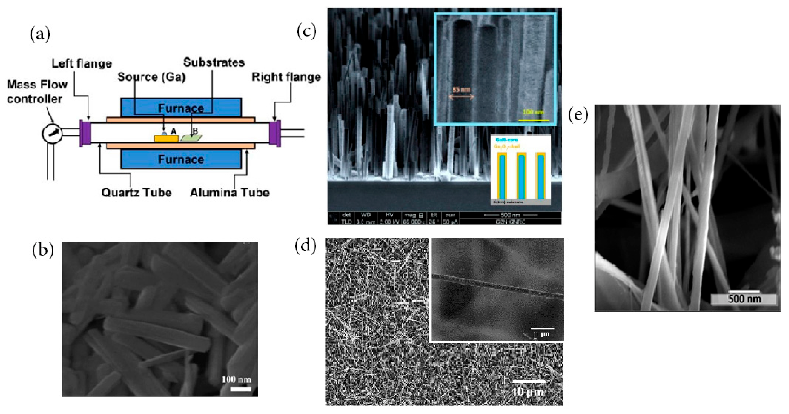
4.1. Bulk Single-Crystal Growth

As for gas sensor applications, a few melt growth techniques have been used for preparing bulk β-Ga2O3 single crystals. These techniques contain the floating zone (FZ) [67,68,69], Czochralski (CZ) [70,71], and edge-defined film-fed (EFG) [52] growths. At high temperatures, β-Ga2O3 single crystal shows an oxygen-sensing property by the electrical resistance measurement. Oxygen diffusion in bulk takes place more likely by interstitial migration rather than by vacancy migration. The hydrogen-sensing characteristics of Pt Schottky diodes have been investigated using ( 2 ¯ 01) and (010) β-Ga2O3 single crystals grown by the FZ and EFG methods. Different gallium and oxygen atomic configurations of Ga2O3 surfaces result in somewhat distinctive hydrogen responses of ( 2 ¯ 01) and (010) facets. However, it remains unknown which is the chemical active crystal face of β-Ga2O3. The carrier mobility in single-crystal and polycrystalline ceramics was shown to be identical by the high-temperature Hall measurements [57]. Therefore, Ga2O3 polycrystalline thin films and nanostructures have become more popular than bulk crystals for advanced gas sensors. Since there have been quite a bit of research on gas-sensing characteristics of β-Ga2O3 single crystals, the bulk crystal growth methods of Ga2O3 are not discussed in detail here and can be found in other reviews [3,14,15,16,36]. Numerous approaches have been employed for the preparation of Ga2O3-sensing materials in the form of thin film and nanostructures. Later on, we will focus our discussion on the four most prevalent synthesis routes in the literature: magnetron sputtering, chemical vapor deposition (CVD), sol–gel synthesis, and hydrothermal synthesis.

4.2. Magnetron Sputtering

One of the most popular techniques for the growth of Ga2O3-sensing material is magnetron sputtering because of its low cost, simplicity, and low operating temperature. It is a physical vapor deposition technique to deposit thin films in which atoms are removed from a sintered target by bombardment with positive gas ions such as Ar+. A magnetic field is added beneath the target to create plasma at lower working pressures and to deflect and confine electrons. Since gallium has a low melting point of 29.8 °C, Ga2O3 thin films can be sputtered only from the metal oxide target. A radio frequency (RF) voltage is usually applied in order to prevent the target from charging up due to the bombardment from positively charged ions, as the Ga2O3 target is an insulating ceramic one. Saikumar et al. [24] provided a review of RF-sputtered films of Ga2O3 and clarified the influences on the crystallinity and film properties of Ga2O3 from various sputtering parameters, such as substrate temperature, sputtering power, annealing temperatures, and oxygen partial pressure in the reactive sputtering.
Different substrates such as sapphire [72,73,74,75,76,77,78,79,80,81,82,83,84,85,86,87,88], BeO [41,42,89,90,91,92,93,94,95,96,97], silicon [98,99,100,101], and quartz glass [101,102,103,104] frequently equipped with an interdigital electrode have been chosen to deposit Ga2O3-sensing layers using the sputtering technique. The obtained films are polycrystalline or amorphous Ga2O3 thin films. After post annealing, the sputtering β-Ga2O3 polycrystalline films are very suitable for making high-temperature sensors owing to their low-term chemical stability. Ga2O3 with incomplete crystallinity or the amorphous phase has also aroused interest in a room temperature ozone sensor due to the large base resistance and oxygen vacancies [64]. Figure 5 shows the AFM images and XRD patterns of the Cr-doped β-Ga2O3 thin films synthesized on the sapphire substrates by means of RF magnetron sputtering of the Ga2O3 target in oxygen–argon plasma. After annealing, the Ga2O3 thin films with and without the addition of Cr dopant had a β-phase polycrystalline structure, and the average grain size was estimated to be 90–100 nm for pure β-Ga2O3 and 25–50 nm for Cr-doped β-Ga2O3. However, the main drawback for gas sensor applications is that the sputtered films are too compact to increase the specific surface area.

4.3. Chemical Vapor Deposition

Chemical vapor deposition (CVD) is particularly interesting not only because it gives rise to high-quality Ga2O3 thin films and nanostructures but also because it is applicable to large-scale production [105]. CVD, also referred to as chemical vapor transport or vapor phase epitaxy, is a conventional method often using a multitemperature zone tubular furnace (see Figure 6a) or a stainless steel chamber as a reactor. As metal organic precursors are used, the CVD technique is called MOCVD, while, in the case of hydride or halide precursors, the technique is named HVPE. Strictly speaking, thermal oxidation should not belong to the CVD technique. It will be discussed together in this section due to the high growth temperature and chemical reaction in an activated gaseous environment similar to CVD. In the CVD process, the reactant gases are diluted in carrier gases and introduced into the reaction chamber or region. When the reactant gases approach the surface of the heated substrate, chemical reactions occur on the surface to form the deposited material. The energy necessary to start the desired chemical reaction can be supplied as thermal energy or photon energy or glow discharge plasma. Gaseous reaction by-products are then evacuated with the carrier gas by a rotary pump.
For the growth of Ga2O3-sensing material, liquid gallium [106,107,108,109,110,111,112,113,114,115,116,117,118,119,120,121,122,123], gallium nitride [124,125,126,127,128,129,130,131,132], gallium sulfides, including Ga2S3 [133] and GaS [134], gallium acetylacetonate [135], and gallium chloride [65,66,136,137,138] are often used as the gallium source, while pure oxygen or water vapor is selected as the oxygen source. Argon or nitrogen is used as the carrier gas. Sometimes, a mixture of Ga2O3 and carbon powders was also used as the precursor material to fabricate Ga2O3 nanostructures [139,140,141]. The key growth parameters, including precursors, growth temperature, growth pressure, growth duration, and gas flow rate, as well as separation distance between the metal source and substrate, all play important roles in depositing Ga2O3. Mostly, β-Ga2O3 nanostructures in the forms of nanowires, nanobelts, and nanorods will be possibly obtained, determined by the vapor–liquid–solid (VLS) or vapor–solid (VS) growth mechanisms [11]. Figure 6b–e shows some newly CVD-deposited Ga2O3 nanostructures, such as nanowires, nanorods, nanobelts, nanoribbons, and core–shell nanowires in recent years. Although a large variety of Ga2O3 nanostructures can be grown epitaxially on substrates using CVD, its disadvantage is that a high operating temperature is required, and the by-product gas may be hazardous and harmful.
Figure 6. (a) Schematic experimental setup of the CVD furnace for the growth of Ga2O3 nanostructures [11]. Copyright 2013 Wiley. (b) SEM image of β-Ga2O3 nanorods [135]. Copyright 2016 The Royal Society of Chemistry. (c) SEM image of GaN/Ga2O3 core–shell nanowires [131]. Copyright 2019 MDPI. (d) SEM and HR-TEM images of β-Ga2O3 nanowires [140]. Copyright 2020 Elsevier. (e) SEM image of SnO2-coated β-Ga2O3 nanobelts [132]. Copyright 2021 Elsevier.
Materials 15 07339 g006

4.4. Sol–Gel Synthesis

Of all the solution synthesis approaches, the sol–gel method is the most extensively used method to synthesize metal oxide-sensing material, since it allows for exquisite control over the size, shape, and crystal phase of the resultant material. The sol–gel process usually involves several steps: (i) dispersion of colloidal particles in a liquid to form a sol, (ii) deposition of the sol solution on a substrate by spraying or dipping or spinning, (iii) polymerization of the particles in the sol to become a gel by stabilizing the removal of the component, and (iv) pyrolysis of the remaining organic or inorganic components, thus forming the final film. Inorganic metal salts or metal organic compounds, e.g., gallium nitrate [142,143,144,145] and gallium isopropoxide [146,147,148,149,150,151,152], were commonly available precursor solutions used in the sol–gel process of Ga2O3-sensing material. The sol–gel synthesis of Ga2O3 films depends on the solvent, pH value, viscosity, temperature, and so on. The surface morphology and crystallinity can be modified by subsequent heat treatment. However, disadvantages such as weak adhesion and low wear resistance limit its application in sensor fabrication.

4.5. Hydrothermal Synthesis

Due to easy operation and tunable growth parameters, hydrothermal synthesis is an important approach for the preparation of nanocomposites for gas sensor application. The hydrothermal process begins with an aqueous mixture of soluble metal salt precursors. Then, the solution is placed in an autoclave for reaction under relatively high pressure and moderate temperature conditions. In most cases, gallium nitrate hydrate Ga(NO3)3xH2O [153,154,155,156,157,158,159,160,161,162] was used as the precursor for synthetizing Ga2O3 nanomaterials. The chosen solution has been always distilled water, while other organic solvent such as alcohol [156,157] was also used. After hydrothermal growth, the precipitates were calcinated for a couple of hours to improve the crystallinity. To obtain Ga2O3-sensing material with a certain size and morphology, it needs to precisely modulate the PH value and concentration of the solution, temperature, pressure, and reaction time. However, it is difficult to control the tailored phases and exact morphologies. Pilliadugula and Krishnan [159] studied the effect of PH on the surface morphology of hydrothermal synthesized β-Ga2O3 powders. Figure 7 shows the morphology evolutions of the as-prepared samples at different PH values. It was demonstrated that an extremely alkaline solution (PH = 14) caused higher-order hierarchical structures, whereas the acidic solution (PH = 5) facilitated nanorod structures. Cocoon-shaped morphology was formed as the PH value was increased from 7 to 11.

4.6. Other Methods

Besides the above-discussed methods, there have been other vacuum and nonvacuum growth techniques, such as pulsed laser deposition (PLD) [163,164,165,166,167], atomic layer deposition (ALD) [168], coprecipitation [169,170], and spray pyrolysis [171], for the fabrication of Ga2O3-sensing material. Photoelectrochemical oxidation [172,173,174] was also used to grow Ga2O3 thin films on the GaN surface. In this process, the GaN epitaxial film was dipped into a phosphoric acid solution and then oxidized under the illumination of a He-Cd laser source with wavelength of 325 nm. An amorphous Ga2O3 film was directly grown and could be converted to the β-Ga2O3 phase by annealing in O2 or N2 ambiance. Recently, a novel liquid gallium-based sonication approach [175,176,177] was developed to prepare Ga2O3 thin films with lots of microparticles. Using this approach, ternary alloy oxides with tuning compositions were achieved by the probe sonication of liquid gallium with traces of In, Sn, and Zn in the water medium or other solvents. After annealing, the as-prepared samples can be applied for sensing NO2 at a low temperature.

5. Ga2O3-Based Gas Sensors

Over the past three decades, several types of gas sensors using Ga2O3 bulk crystals, thin films, and nanomaterials have been developed to detect diverse oxidizing and reducing gases during a wide operational temperature range from room temperature to more than 1000 °C. In this section, we will focus on the advances in Ga2O3-based gas sensors, which cover the fundamentals of semiconductor metal oxide gas sensors and the prevailing strategies for how to improve the performance of Ga2O3 gas sensors.

5.1. Sensing Mechanisms

Gas-sensing mechanisms explain why the gas can cause changes in the electrical properties of a sensor. Several common gas-sensing mechanisms of metal oxide semiconductor gas sensors were reviewed by Ji et al. [178] in detail. However, the mechanisms governing Ga2O3-based gas sensors seem quite different. Most gas sensors using Ga2O3 are based on the resistive or conductive change upon target gas exposure. The sensing mechanisms of conductivity for Ga2O3-based gas sensors can be found in Refs. [3,26,179,180,181]. As mentioned above, the conductance of n-type Ga2O3 is determined by the carrier concentration and electron mobility. Both of them are temperature-dependent. When detecting gas, the change in conductance of Ga2O3 is dominated by the variation of electron density at a high temperature, while the influence of the conductance of Ga2O3 from electron mobility at a low temperature is more distinctive. As far as the mechanism that describes the interaction between the target gas and the sensitive metal oxide is concerned, three temperature-dependent regimes can be distinguished for Ga2O3-based resistive gas sensors [4,26,179,180,181,182] from Figure 8a.
In a high operating temperature range above 800 °C, the oxygen in the surrounding atmosphere and in the crystal lattice is in dynamic equilibrium, which means the oxygen exchange undergoes constantly between the bulk lattice of Ga2O3 and the ambient. If there is a reduction in the proportion of oxygen in the surrounding atmosphere, Ga2O3 crystal will experience an increase in the concentration of positively ionized oxygen defects in the lattice. Using the Kröger–Vink notation, the sum of the processes can be described as [180]
Ga 2 O 3 2 Ga Ga x + 2 O O x + V O * + e + 1 / 2 O 2 g .
As a consequence, the conductivity of Ga2O3 increases because of the delocalized electrons in crystal lattice. It can be said that this sensing regime is dominated by bulk oxygen defects. One can use it to implement high temperature oxygen sensors, which obey a typical power law [26,99,183]
σ p O 2 m e E A / k T ,
where pO2 is the oxygen partial pressure and EA is thermal activation energy of a dopant, k is the Boltzmann constant, and T is the temperature. The first part in above equation represents the contribution from the oxygen partial pressure, and the last part reveals the temperature dependence of the conductivity on the doped specimens.
In the intermediate operation temperature range below 800 °C, only an exchange of oxygen near the surface of Ga2O3 with the surrounding gas takes place. If a certain reducing gas such as CH4 approaches the surface, it will be oxidized by oxygen from the near-surface region, leading to the formation of oxygen vacancy donors at surface and a greater conductivity due to the release of conduction electrons. The process then will be recovered in the absence of reducing gas, since the loss of oxygen of the Ga2O3 surface is compensated by the oxygen from the ambient atmosphere. In this case, the sensing regime is mainly caused by surface oxygen defects.
At even lower temperatures, the oxygen defect equilibrium disappears. The gas-sensing behavior is dominated by the change in electron mobility controlled by grain boundaries, rather than the change in oxygen defect-affected charged carrier density. As shown in Figure 8b, on the one hand, similar to other metal oxides, a potential barrier is formed at the grain boundary of Ga2O3 by pre-adsorbed oxygen ions with negative charge in the air, leading to a charge depletion region between grains. The adsorbed oxygen ions are O2 below 200 °C, O in the range of 200–550 °C, and O2− above 550 °C. The width of charge depletion region is determined by the Debye length [26]:
L D = ε k T / n e 2 ,
where ε is the permittivity, n is the electron density, and e is the electronic charge.
When exposed to a reducing gas such as CO, the gas molecules react with chemisorbed oxygen ions at the Ga2O3 surface and return the captured electrons to the conduction band, resulting in the decrease of the depletion width. Hence, the conductance is increased due to the easier electronic transport across the grain boundary. In the case of the presence of an oxidizing gas such as NO2, a competitive adsorption process may take place, and the overall results are a wider depletion region, smaller electron mobility, and a decrease of conductivity. However, the sensitivity toward NO2 could be very low, since the Debye length of Ga2O3 is as large as several μm [181].
On the other hand, reducing a gas such as H2 will be chemisorbed at the surface via covalent bonds to form adsorbed molecules with positive charges. To satisfy the electric neutrality, more conduction electrons are released, yielding a conductive increase in n-type Ga2O3. The chemisorption process happens even with no oxygen in the ambient. However, the overall concentration of the surface adsorbed species is subject to the Weisz limit [184]. Clearly, gas chemisorption and reaction at the surface play an important role in this low-temperature-sensing regime.
It should be noted that there are no upper and lower temperature limits for the three gas-sensing regimes. The modulation of the conductance of Ga2O3 by the target gas can be a consequence of one or a combination of grain boundaries, gas absorption and reaction, and oxygen vacancies. There have also been various Ga2O3-based nonresistive gas sensors using different operating principles. For example, the gas-induced changes in work function, in capacitance, in the Schottky potential barrier, and in the ionic conductivity can be used for sensing a wide range of target gases. These gas-sensing mechanisms are similar to those of other semiconductor metal oxide sensors, which can be easily found in a lot of the literatures such as [185].

5.2. Evaluation Criteria

Usually, the performance of Ga2O3-based gas sensors can be evaluated with respect to the ‘4s’-criteria: sensitivity, speed, selectivity, and stability [43].
The sensitivity S, also named as response, in the presence of gases is usually defined in several different forms. It is generally calculated from the ratio of the electrical readout (resistance R or conductance G and current I or volt V) of the sensor in background gas (usually air) Ya to that upon exposure to certain concentrations of the target analyte Yg:
S = Y a / Y g ,
for oxidizing the target gas and
S = Y g / Y a ,
for reducing the target gas.
Other expression forms of sensitivity that describes the variation degree of the output signal are also in use:
S = Δ Y a / Y g .
The detection speed is evaluated by the response and recovery time. The response time is defined as the time required for a sensor to reach 90% of the total response upon exposure to the target gas. Recovery time is defined as the time required for a sensor to return to 90% of the original baseline signal upon removal of the target gas.
The selectivity of a sensor describes how much the sensor is disturbed by interfering gases from the target gas. The selectivity Q, which reflects the ability of a sensor to differentiate between the target gas x and the other components in the gaseous environment x′, can be expresses as:
Q = S x / S x .
Obviously, larger Q means better selection of target gas and stronger resistive to interfering gas.
The stability (reproducibility) describes the endurance of a gas sensor to maintain its output signal over a long period of time and/or to the analyte gas of varying concentrations. The stability is greatly affected by thermal aging and gaseous poisoning of the sensor layer, especially when operating in a harsh environment.
Additionally, the operating temperature, power consumption, size, and cost are the other concerns that should be considered, depending on particular applications of gas sensors. It is difficult to achieve all the optimal results of the above performance parameters at the same time. Therefore, to keep the balance according to the specific situation and requirements has become a major aim for the development of Ga2O3 gas sensors.

5.3. Classification of Ga2O3-Based Gas Sensors

According to the famous Yamazoe model [186], a gas sensor can be considered as an integration of a receptor and a transducer. The former is provided with a material or a material system that interacts with a target gas and thus induces a change in its own properties or emits heat or light. The latter is a device to transform such an effect into an electrical signal. There are various approaches used for gas sensor classification. In terms of transduction principles, the gas sensors that many groups have always developed using Ga2O3 as sensing materials can be classified into three categories: electrical gas sensors, electrochemical gas sensors or solid electrolyte-based gas sensors, and optical gas sensors [187].

5.3.1. Electrical Gas Sensors

Electrical gas sensors, operating due to electronic conduction induced by a surface interaction with target gas, contain resistor-type gas sensors and nonresistive sensors such as SBD-, FET-, and capacitor-type gas sensors.
(1) Resistor-type gas sensors are the conductometric sensors that measure the change in resistance caused by the interaction between the sensing element and analyte gas. They possess advantages such as simple configuration, easy fabrication, and cost effectiveness and can be easily miniaturized and integrated on a microelectronic mechanical system platform. A typical resistor-type gas sensor based on Ga2O3 is depicted in Figure 9a. Pt and Au are commonly used as measuring electrodes, since the electron affinity of Ga2O3 is as large as about 4 eV [40]. Similar to solar-blind ultraviolet photodetectors, the interdigitated electrode geometry, which enables a wide contact area, is the most widely accepted geometry for a resistor sensor. In most cases, it forms the electrodes first and then deposits the Ga2O3-sensing layer on them, thereby causing no damage to the sensing material. Additionally, a Pt heater is placed on the back side of the substrate to heat the sensor.
In early years, Fleischer and Meixner in Siemens AG and their cooperators adopted the RF magnetron sputtering technique to fabricate β-Ga2O3 polycrystalline thin films and constructed resistor sensors to detect a variety of gases, such as O2 [41,42,74,79,96,102,188,189,190]; O3 [81]; H2 [74,78,79,82,89,90,95,191,192,193,194]; CO [75,79,82,89,91,97,188,189,191,192]; NO [78,79,96]; NH3 [79,96]; and hydrocarbons (HCs) such as CH4 [73,77,78,79,82,94,97,102,188,189,195], C3H8 [79,82,196], and C4H8 [79,188], as well as volatile organic compounds (VOCs) such as C2H6O [78,79,97,195] and C3H6O [78,80,82]. The operating temperature ranges from 1100 °C to 400 °C. Typically, polycrystalline Ga2O3 thin films can be used either for sensing oxygen (>900 °C) or reducing gases (<900 °C) [14,91]. The co-adsorption of H2O and other coexisting gases of the sputtered films were considered by Giber et al. [197], Reti et al. [198,199,200], and Pohle et al. [201]. Due to a high operating temperature, a self-cleaning effect was observed on the sensor surface, and the unwanted species could be eliminated to a large extent. Varhegyi et al. [202] investigated the influence from corrosive gases such as Cl2 and SO2 on the Ga2O3-sputtered layer and found that Ga2O3 was more resistant against SO2 but had a very fast reaction with Cl2 at 800 °C. A screen-printing technique was developed by Frank et al. [188], Pole et al. [201], Wiesner et al. [195], and Biskupski et al. [196] to prepare porous Ga2O3 thick films for detecting oxidizing gases such as CO2 and O3 and inflammable gases such as C4H10 and C3H8, as well as VOCs. Additionally, many other groups such as Macri et al. [72], Ogita et al. [62,63,97,103], Hovhannisyan et al. [203], Dyndal et al. [204], Almaev et al. [86,87], Manandhar et al. [101], and Sui et al. [64] studied the gas sensitivities of resistor sensors with sputtering films for O2, H2, CO, C7H8, C2H6O, and C3H6O. However, it is very hard to reduce the operating temperature of these resistor sensors using the Ga2O3 compact films to a lower value.
With the progress of advanced synthesis technologies, many novel Ga2O3 nanomaterials with different compositions and microstructures have been prepared for resistor sensors. The morphology of these Ga2O3 functional nanomaterials varies from one dimensional to three-dimensional nanostructures such as nanospheres, nanoflowers, nanowires, nanorods, nanobelts, and so on. These sensing materials showed high resistive response towards O2 [109], CO [109,124,129,135,140,154,155], CO2 [158], H2 [113,132,176], NH3 [159,162,177], NO2 [125,126,128,141,160,161,176], VOCs such as C2H6O [117,123,141,168], C3H6O [123,133,157], C3H8O [120], and water vapor [127,130,134], as reported by many authors. The operating temperature can be low to room temperature due to the large specific surface area and robust properties of nanostructures.
(2) Since Lundstrom et al. [205] first achieved a H2-sensitive Pd-gate gasFET device, there has been of great interest in semiconductor metal oxide nonresistive-type gas sensors due to the simple electrical circuit required to operate them. In contrast to the above-discussed resistor-type gas sensors, the gas-sensing properties of nonresistive ones will be less affected by the morphology of Ga2O3-sensing material. In generally, nonresistive type gas sensors consist of two types of structures, i.e., metal/semiconductor (MS) is metal/insulator/semiconductor (MIS) structures. Comparatively, the MIS structure is always adopted in designing Ga2O3 sensors with Pd or Pt as catalytic metals and Ga2O3 as reactive insulator material. There are usually three types of nonresistive-type gas sensors based on various operating principles, namely, SBD-type, FET-type, and capacitor-type gas sensors. Figure 9b–d depict the schematic device structures of these three typical Ga2O3-based nonresistive-type gas sensors. The basis with respect to SBD- or FET-type (including MIS capacitor) gas sensors with a catalytic metal is modulation in the Schottky barrier height or the flat band potential by target gas [187]. Catalytic decomposition of hydrogen on the surface of noble metal and subsequent diffusion of hydrogen atoms to the interface between metal and insulator make these devices respond to H2 and many hydrogen containing gases.
SBD-type sensors operate on the change in Schottky barrier height affected either by formation of a dipole layer or by modification of work function once gaseous species interact with the metal surface. Then, the gas-induced rectifying property can be recognized by I–V characteristics under a forward, as well as reverse, bias voltage. Pt/Ga2O3/SiC [146,149,150,151,152] and Pt/Ga2O3/GaN [172,173,174] Schottky diode gas sensors were built to detect H2 and C3H6 at different operating temperatures. Notably, Jang et al. [52] and Nakagomi et al. [68,69] reported Schottky diode gas sensors based on β-Ga2O3 single crystals, which showed an enhanced response to H2 and stable operation at elevated temperatures. Almaev et al. [136] studied the gas-sensing properties of Pt/α-Ga2O3: Sn/Pt Schottky metal–semiconductor–metal structures when exposed to H2, O2, CO, NO, CH4, and NH3 in the temperature range of 25–500 °C.
FET-type sensors are based on the readout of work function change of the sensing material. The gas response of FET-type sensors is measured as a shift in either gate-source voltage or drain-source current, and it has been shown that this response is related to a shift in the threshold voltage. This kind of gas sensors can detect many reducing gases, such as H2 and VOCs. A hybrid FET-type sensor was designed using Ga2O3 as the sensitive layer and the measured variation of the work function indicated a multiple response to H2, NH3, and NO2 [206,207,208]. In their work, an analytic theoretical model was proposed to explain the inner sensing mechanism. Lampe et al. [84] made a gas FET sensor in which a sputtered Ga2O3 thin film activated with Pd was used to detect CO. Stegmeier et al. [85,86] used sputtered Ga2O3 film to construct a FET-type sensor for detecting VOCs. Nakagomi et al. [118,119] reported a field–effect hydrogen sensor using Ga2O3 thin film prepared by CVD. Shin et al. [209] investigated the channel length scaling effects on the signal-to-noise the ratio of a FET-type NO2 sensor. It was demonstrated that the FET gas sensors had an advantage of working at room temperature.
MIS capacitor-type sensors are changes that can be made to the relative permittivity of the dielectric, the area of the electrode, or the distance between the two electrodes and, therefore, by measuring the change in the capacitance. Arnold et al. [110] reported an interdigital comb-finger structural capacitor gas sensor with β-Ga2O3 nanowires as dielectric. By capacitance measurement using a balanced AC bridge circuit, the sensor showed a rapid and reversible response to VOCs such as C2H6O and C3H6O and a more limited response to some HCs, including C7H8 at room temperature. Mazeina et al. [114,115] compared pure and functionalized Ga2O3 nanowires as active material in room temperature capacitance-based gas sensors. It was found that the functionalization of Ga2O3 nanowires with acetic acids showed a significant decrease in response to C3H8O and CH₃NO₂ as well as C₆H15N. In the case of pyruvic acid-functionalized nanowires, no response was observed to CH₃NO₂, but one order of magnitude increased response to C₆H15N was obtained compared to the pure nanowires.

5.3.2. Electrochemical Gas Sensors

An electrochemical gas sensor is a device that yields an output as a result of an electrical charge exchange process at the interface between ionic or electronic conductors. Solid electrolytes exhibit high ionic conductivity resulting from the migration of ions through the point defect sites in their lattices. In solid electrolyte-based sensors, electronic conduction only makes typically less than 1% contribution to the total conductivity, while the ionic conductivity contributes to 99% of the rest. Schematic device structures for two kinds of electrochemical gas sensors containing Ga2O3 are shown in Figure 10. In an early study, NH4+ ion conducting gallate solid electrolyte was prepared by mixing K2CO3, RbCO3, and Ga2O3 [210]. Fabricated by the combination of NH4+-Ga2O3 and rare earth ammonium sulfate as a solid electrolyte and a solid reference electrode, the gas sensor showed outstanding NH3 detection in good accordance with the Nernst relation. In a mixed potential gas sensor based on O2− ion conducting yttria-stabilized zirconia (YSZ) solid electrolyte, Ga2O3 was used to stabilize the metal (Au, Pt) electrode in its morphology and to inhibit its catalytic activity [211,212,213,214,215]. The results indicated that these gas sensors had a high sensitivity and good selectivity of HCs, such as C3H6. An electrochemical Pt/YSZ/Au-doped Ga2O3 impedance metric sensor was fabricated by Wu et al. [216]. The impedance of the sensor originated from the Ohmic contact resistance, the electrolyte impedance, and the interfacial impedance between the electrolyte and the sensing electrode. Strong dependence of the interfacial impedance upon the CO concentration at 550 °C was found due to an electrochemical oxidation of CO. Yan et al. [217] synthesized a mesoporous β-Ga2O3 nanoplate to make an amperometric electrochemical sensors. It was summarized that more oxygen defects and action sites in β-Ga2O3 nanoplate account for enhanced gas sensitivity in detecting CO.

5.3.3. Optical Gas Sensors

Optical gas sensors detect changes in visible light or other electromagnetic waves during interactions with gaseous molecules. Reiprich et al. [122] used a corona discharge assisted growth morphology to prepare Sn-doped Ga2O3 for optical gas-sensing application. The Sn-doped Ga2O3 layer was shown to be capable of detecting small amounts of C2H6O, C3H6O, and C3H8O at room temperature. The reason was that the generation and quantity variance of negatively charged oxygen ions indirectly produced a change in the photoluminescence spectrum. It was also observed that the response toward C3H6O of a Ga2O3 layer-like structure would be increased by 30% relative to the nanowires. However, the study of Ga2O3-based optical gas sensors is in its infancy, further careful investigations are needed into this type of gas sensor.
To sum up, Ga2O3-based gas sensors exhibit broad-range sensitivity to a wide variety of analyte gases. Table 3 lists the available target gases of different types of Ga2O3-based gas sensors. The most preferable target gases are O2, CO, H2, and CH4 [218].

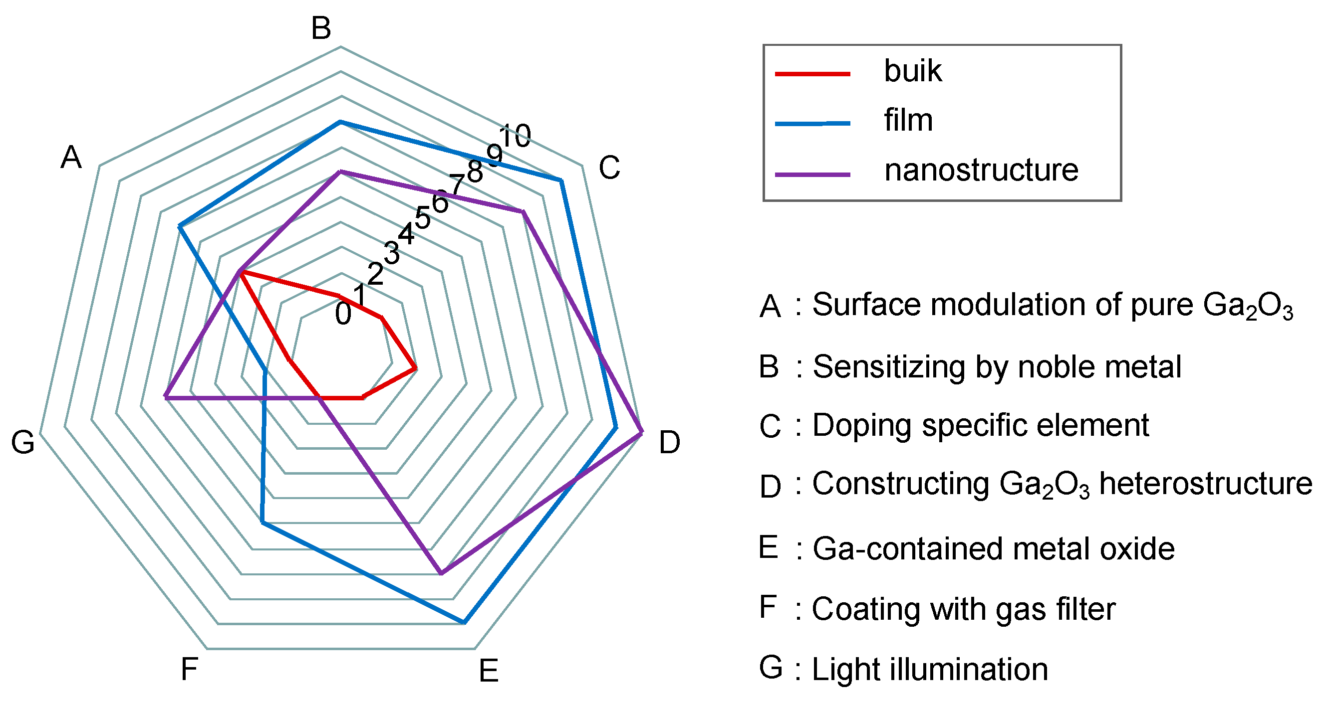
5.4. Performance Enhancement Strategies

As is discussed in the former section, Ga2O3 can be used to make several types of gas sensors that respond to lots of gases, ensuring a wide application range. However, Ga2O3-based gas sensors still encounter some issues such as low selectivity, average sensitivity, and high operation temperature [26,182,187,218]. Multiple ways have been developed till now by many researchers to improve the gas-sensing performance of Ga2O3-based gas sensors through material engineering and device optimization.

5.4.1. Surface Modulation of Pure Ga2O3

It is well-known that the performance of Ga2O3 gas sensors greatly depends on the interaction between target gas and the Ga2O3 surface. Therefore, surface modulation, such as crystallinity, porosity, and oxygen vacancies, in the process of fabricating Ga2O3-sensing material plays an important role in determining the gas-sensing behavior. Ogita et al. [63,67,99,100,219] presented a series of studies on the influence of the annealing conditions on the high-temperature oxygen-sensing properties of the Ga2O3 thin film sensor. The results indicated that the annealing conditions affect not only the grain size, number of oxygen vacancies and surface roughness but also the oxygen-sensing properties of Ga2O3 thin films. The oxygen sensitivity of the sensors increases when the oxygen flow rate was increasing from 0 to 100% at 1000 °C. The response time of the Ga2O3 sensors decreased as the grain size increases with increasing the annealing temperature and annealing time. The authors also measured the oxygen-sensing characteristics at 1000 °C for β-Ga2O3 sputtered thin films and β-Ga2O3 single crystals and found that both sensors had response times in the same range. Grain boundaries played an important role in determining the value of the response time in sputtered films, while the surface processes primarily influenced the modifications of the resistance for single crystals. The influence of film thickness on sensing response at room temperature was investigated by Pandeeswari and Jeyaprakash [171]. The sensitivities towards 0.5 ppm and 50 ppm of NH3 increased as the film thickness became larger.
Due to large surface to volume ratio and abundant surface active sites to the target gas, porous and nanostructured Ga2O3 was always used as the sensing layer. Cuong et al. [113] addressed the effect of growth temperature on the microstructural properties and H2 sensing ability of Ga2O3 nanowires. Girija et al. [135] performed the gas-sensing analysis of morphology-dependent β-Ga2O3 nanostructure thin films. It can be seen from Figure 11 that nanorods of β-Ga2O3 had a higher surface area with a larger pore volume distribution than rectangular β-Ga2O3 structures. As a result, rod shaped β-Ga2O3 nanostructures showed better sensitivity, shorter response, and recovery time upon exposure to CO gas at 100 °C in comparison with rectangular shape β-Ga2O3 nanostructures. The improvement on sensor performance could be contributed from the high surface area, particle size, shape, numerous surface active sites and the oxygen vacancies. The effect of pH-dependent morphology evolutions on room temperature NH3-sensing performances of β-Ga2O3 nanostructured films was investigated by Pilliadugula and Krishnan [159]. It could be seen that the sample with hierarchical morphology and relatively low crystallite size showed utmost sensing responses at all concentrations of NH3 relative to the remaining samples.
High-energy crystal facet has a higher surface energy and more defect sites, thus exhibiting more active physicochemical properties and better gas-sensing performance. Jang et al. [52] demonstrated that the H2 responses of the (010) facet were slightly higher than that of the ( 2 ¯ 01) facet when studying the sensing characteristics of Schottky diode-type gas sensors using Ga2O3 single crystal. However, it is not clear which facet is the most active one for gas sensors so far.

5.4.2. Sensitizing by Noble Metal

In most of gas-sensing process, small noble metal nanoparticles or clusters distributed on the surface of Ga2O3 can improve the efficiency of catalytic reactions between target gases and the surface of sensing layers, thus remarkably enhancing the gas-sensing characteristics. At an early stage, Fleischer et al. [91], Bausewein et al. [74], and Schwebel et al. [75] studied the effects of Pt, Pd, and Au catalyst dispersions on the sensitivity to reducing gases of high temperature Ga2O3 thin film sensors. They found that Pt dispersion accelerated the response of CO, whereas significantly increased the sensitivity to H2. Au clusters on the Ga2O3 surface could yield a high sensitivity to CO and a distinct reduction of the cross-sensitivity towards VOCs. However, although Pt accelerated the desorption of H2 on Ga2O3, it had no impact on the sensitivity to H2. Recently, Krawczyk et al. [138] reported the impregnation of Au nanoparticles of the HVPE-prepared n-type β-Ga2O3 layer would cause an inversion to p-type conductivity at the surface. The conductive sensitivity of the Au-modified β-Ga2O3 layer toward 16 ppm of dimethyl sulfide obviously was enhanced if compared to that of the unmodified β-Ga2O3 layer. Pt and Au-decorated Ga2O3 nanowires were synthesized by Kim et al. [124] and Weng et al. [140]. Figure 12 shows the SEM and TEM images and electrical response of the gas sensors fabricated by Pt- and Au-decorated Ga2O3 nanowires. As measuring at 100 °C, the responses of the Pt-functionalized nanowire were reported to improve 27.8-, 26.1-, 22.0-, and 16.9-fold at CO concentrations of 10, 25, 50, and 100 ppm, respectively, relative to the bare Ga2O3 nanowires. However, both the response and recovery times of this Pt-functionalized CO sensor were increased significantly. Through CO gas sensor measurements at room temperature, Au-decorated single β-Ga2O3 nanowire showed better results than single pure β-Ga2O3 nanowire and multiple networked Au-decorated β-Ga2O3 nanowires. The enhancement of the CO-sensing properties was resulted from a combination of the spillover effect and the enhanced chemisorption and dissociation of the target gas.
So far, noble metals had also been used in FET-type and solid electrolyte type gas sensors to catalytically activate the sensing layer. Zosel et al. [212,213] achieved a high sensitivity for hydrocarbons in potentiometric zirconia-based gas sensors, attributed to the catalytic activity of the Au composites. Shuk et al. [215] reported that the mixed potential solid electrolyte sensor based on Au/Ga2O3 composite electrodes had a sensitivity limit of 5 ppm CO and showed good selectivity, reproducibility, and stability in the presence of other combustion gas species. The FET-type sensors thermally activated by Pd and Pt for the detection of reducing gases were studied by Lampe et al. [84] and Stegmeier et al. [85,86]. The results indicated that catalytic Pt dispersions on the micro- and nanoscale caused a remarkable gas response at room temperature to a large variety of hydrocarbons and VOCs with small concentrations (ppb-ppm). Overall, noble metals such as Pt, Pd, and Au play the roles of chemical sensitizers and electronic sensitizers in Ga2O3 sensors.

5.4.3. Doping Specific Element

Doping is an effective way to influence not only the electronic properties but also the structural properties of grains, such as size and shape, leading to the enhancement of sensing behavior. Frank et al. [102,188,189] found that the doping of sputter-deposited polycrystalline Ga2O3 thin films using donor type ions such as Zr4+, Ti4+, and especially Sn4+ caused a modulation of the base conductivity by two orders of magnitude and strong impact on the sensitivity to reducing gases. However, there was no influence on the sensitivity to reducing gases such as CH4 and CO after doping Mg2+ in the Ga2O3 and no influence of whether donor-type or acceptor-type doping concentration on O2 sensitivity at high temperature. However, in the work of Almaev et al. [87,88], the authors stated that addition of Cr stimulated dissociative adsorption of O2 due to its high catalytic activity via a spillover mechanism, leading to a significant increase in the response of to O2 over the temperature range 250–400 °C. The O2 gas-sensing performance of Ga2O3 semiconducting thin films prepared by the sol–gel process and doped with Ce, Sb, W, and Zn was investigated by Li et al. [148]. The authors observed that the operating temperature of sensors doped with Zn reduced below 450 °C and Sensors doped with Ce had a very fast response time of typically 40 s. W-doped sensors showed the highest response to O2 while Sb-doped films possessed the highest base resistance. Sn was proven to be the most effective dopant in Ga2O3 for gas detection at different operating temperatures [121,122,162,170,189]. As examples, Figure 13 exhibits the enhancement of the sensor sensitivity of Sn-doped Ga2O3 gas sensors when detecting different gases. An increase in conductivity of up to two orders of magnitude, as well as an enhancement of the gas sensitivity toward CO and CH4, was found by employing SnO2 as a doping material into sputtered polycrystalline Ga2O3 thin films [189]. Doping Sn could enhance the adsorption of NH3 due to the higher Lewis acidity of Sn4+ cations than Ga3+ ones [170]. Moreover, the introduction of Sn causes a decrease in the average crystallite size and an increase in the specific surface area [162]. Therefore, Sn-doped Ga2O3 NH3 sensor showed better performance than the pure Ga2O3 one regardless of the operating temperature. Manandhar et al. [101] demonstrated that the Ti-doped nanocrystalline β-Ga2O3 films significantly accelerated the oxygen response about 20 times while retaining the stability and repeatability.
It is noted that doping can not only enhance the sensing properties of resistor-type Ga2O3 sensors but also have a great impact on design of novel sensors. Reiprich et al. [122] used Sn-doped Ga2O3 nanostructure for optical gas-sensing at room temperature. The change in the photoluminescence spectra indicated that Sn-doped Ga2O3 was capable of detecting trace amounts of VOCs such as C2H6O, C3H6O, and C3H8O. Saidi et al. [176] developed a novel liquid metal-based ultrasonication process within which additional metallic elements (In, Sn, and Zn) were incorporated into liquid Ga and then sonicated in dimethyl sulfoxide (DMSO) and water. These new types of doped Ga2O3 sensors showed very tuning sensitivities to NO2 and H2. Impedance measurements were performed on the Pt/YSZ/Au-doped Ga2O3 CO electrochemical sensor [216] and on the humidity sensor-based on Ga2O3 nanorods doped with Na+ and K+ [220]. Both types of Ga2O3 gas sensors showed fast response of target gases. Due to the synergistic effect of Ga2O3 nanorods and the doping of alkali metal ions, Ga2O3 nanorod gas sensor exhibited good linearity response and high stability over 25 days. So far, the dopants added in Ga2O3 were Zr, Ti, Mg, Sn, Ni, N, Na, K, Cr, In, Zn, Pt, and Au for the purpose of enhancing the sensing properties.

5.4.4. Constructing Ga2O3 Heterostructure

Semiconducting heterostructures show great potential in gas sensors because of a high surface-to-volume and synergistic effect [221]. Once heterointerface forms, Fermi level-mediated charge transfer and band bending occur, usually resulting in a higher sensitivity. According to the types of participating semiconductors, Ga2O3 heterostructures can be divided into the n–n heterojunction and p–n heterojunction. Figure 14 illustrates the schematic diagram of the energy band structures for such kinds of heterojunctions. Many heterostructures, including heterojunctions and hierarchical heterostructures, have been developed by many researchers to improve the performance of Ga2O3 sensors. In the early years, Fleischer et al. [79,81,96,190] discovered a dramatic influence on the sensitivity and selectivity of Ga2O3 thin film sensors by sputtering different metal oxide, i.e., WO3, Ta2O5, NiO, AlVO4, CeO2, Sm2O3, RhO, RuO, Ir2O3, and In2O3, as the surface modification layer. These types of thin film sensors could be employed as selective oxygen sensors for gas atmospheres with an overall excess of oxygen.
As for resistor-type of gas sensors, TiO2, SnO2, ZnO, WO3, GaN, and GaS were used for constructing n–n heterostructures with Ga2O3 while NiO, CuO, LSFO, and LSCO of perovskite crystal structure for p–n heterostructures. Mohammadi and Fray [143] reported that mesoporous Ga2O3/TiO2 thin film gas sensors had response values of 13.7 and 4.3 to 400 ppm CO and 10 ppm NO2 gas at 200 °C, approximately 55% larger than pure TiO2 sensors. Jang et al. [117], Liu et al. [139], and Abdullah et al. [132] studied the sensing properties of Ga2O3/SnO2 core–shell nanowires and nanobelts. Compared with pure Ga2O3 nanowire sensor, the optimum sensing temperature was reduced by 200 °C for Ga2O3/SnO2 core–shell nanowire sensors that showed the highest ethanol response at 400 °C. Due to the fast physisorption of water and the fast formation of depletion layers caused by the large surface area of the amorphous SnO2 shell and Ga2O3/SnO2 heterojunction, Ga2O3/SnO2 core–shell nanoribbons had a very high sensitivity to humidity with quick response and recovery near room temperature. At 25 °C, the conductivity of this nanoribbon humidity sensor at 75% relative humidity was three orders of magnitude larger than that at 5% relative humidity. The response time and recovery time were approximately 28 s and 7 s, respectively, when the relative humidity was switched between 5 and 75%. The H2 gas sensor based on Ga2O3/SnO2 core–shell nanobelts exhibited significant enhanced performance at room temperature in terms of response, response/recovery time and repeatability. During the exposure of 100 ppm NO2, multiple networked Ga2O3/ZnO core–shell nanorod sensors showed a super response of 32.778% at 300 °C, which was 692 and 1791 times larger than that of bare Ga2O3 and bare ZnO nanorod sensors [126]. The sensor made by a wafer-scale ultra-thin Ga2O3/WO3 heterostructure [168] exhibited about 4- and 10-fold improvement in the response to C2H6O compared to that of pure WO3 and Ga2O3 nanofilm sensors at 275 °C. Furthermore, the Ga2O3/WO3 heterostructural sensor possessed a shorter response/recover time and excellent selectivity. Park et al. [129] developed a Ga2O3/GaN core–shell nanowire sensor by surface-nitridated Ga2O3 nanowire. It showed responses of 160–363% to CO concentrations of 10–200 ppm at 150 °C, which were 1.6–3.1-fold greater than those of pristine Ga2O3 nanowire sensors.
For n–n junction, an accumulation layer is usually created, whereas a depletion layer forms in p–n junction. Lin et al. [154] and Zhang et al. [161] fabricated p–n heterostructural gas sensors using perovskite-sensitized Ga2O3 nanorod arrays for CO and NO2 detection at high temperature. Figure 15 gives the TEM images and measured sensing performances of gas sensors made by Ga2O3/La0.8Sr0.2FeO3 (LSFO) and Ga2O3/La0.8Sr0.2CoO3 (LSCO) nanorods. Compared with the pristine Ga2O3 nanorod array sensor, close to 10 times enhanced sensitivity to 100 ppm CO was discovered for Ga2O3/LSFO sensors at 500 °C. In addition to the excellent CO sensitivity, the sensor based on Ga2O3/LSFO p–n heterostructure has a faster response time than that of the pristine Ga2O3 sensor. Ga2O3/LSCO sensors also showed nearly an order of magnitude enhanced sensitivity to 200 ppm NO2 at 800 °C, along with much shorter response time. Ga2O3/CuO thin films were magnetron sputtered by Dyndal et al. [204] as a gas-sensitive material for C3H6O detection measured at 300 °C. Benefited from p–n heterostructure, Ga2O3/CuO thin film sensor exhibited 40% faster response time in comparison with pure CuO one. Sprincean et al. [134] made a Ga2O3/GaS:Zn nanostructured room temperature humidity sensor, which demonstrated acceptable sensitivity on the air relative humidity in the range from 42 to 92% and stable static characteristics over 6 months.
Additionally, Wang et al. [160] investigated the gas-sensing behavior of Ga2O3/Al2O3 nanocomposite and found that the composite-based sensor had a 6.5 times higher response to 100 ppm NOx than that of the pure Ga2O3 sensor at room temperature. Notably, Sivasankaran and Balaji [177] synthesized mesoporous Ga2O3/reduced graphene oxide (rGO) nanocomposites by hydrothermal method. The results indicated that the sensing response to 200 ppm NH3 of Ga2O3/rGO nanocomposite was 3.7-fold larger than that of pure Ga2O3 at room temperature.
As known, Ga2O3-based Shottky diode H2 sensors generally has the MIS-type heterostructure in which β-Ga2O3 is served as reactive insulator and SiC [146], GaN [172,174], and AlGaN [173] are chosen as semiconductors. Lee et al. [174] concluded that the MIS-type sensor diodes exhibited better forward response than the MS-type Schottky sensor diode, because the β-Ga2O3 insulator surface provided more trap sites for hydrogen atoms at the metal–insulator interface.

5.4.5. Ga-Contained Metal Oxide

Aside from doping in Ga2O3, the gas-sensing properties can be optimized by intentional doping Ga3+ or solubility of Ga2O3 into other metal oxides. In general, host metal oxides are In2O3 [141,156,163,164,165,166,167,222], SnO2 [223,224,225], and ZnO [145,226,227,228,229] for resistor gas sensors. Gas sensitive properties of Ga-doped In2O3 thin films and nanostructures were studied by Ratko et al. [222], Chen et al. [156], and Demin et al. [163,164,165,166,167]. Ga2O3 caused the formation of a porous or nanostructure in the In2O3-based ceramics, providing an active surface for reducing gases such as CH4 [222] and CH2O [156]. The response toward 100 ppm CH2O of GaxIn2-xO3 nanofiber was about four times higher than that of pure In2O3. Meanwhile, it has superior ability to selectively detect CH2O against other interfering VOCs. Demin et al. [163,164] obtained a high selectivity to NH3 against C2H6O, C3H6O and liquefied petroleum gas based on 50% In2O3-50% Ga2O3 thin film-sensitive layer. The sensitivities towards O2, CO, C2H6O, and CH2O of Ga-doped SnO2 materials were investigated by Silver et al. [223], Bagheri et al. [224], and Du et al. [225]. The Ga-doped SnO2 thin film O2 sensor showed sensitivity up to 2.1 for a partial pressure of oxygen as low as 1 Torr [223]. Bagheri et al. [224] observed the highest responses of 315 and 119 for 300 ppm CO and C2H6O by the SnO2 sensors containing 5 and 1 wt% Ga2O3, respectively. With adding more than 25 wt% Ga2O3, the sensors became selective to CO and showed negligible responses to C2H6O and CH4. The sensitivity to 50 ppm CH2O of Ga-doped SnO2 sensor was 4.5 times greater than that of the pure SnO2 sensor. Moreover, it exhibited a lower detection limit of 0.1 ppm CH2O with sensitivity of 3 and a short response-recovery time (3/39 s) and good selectivity. Ga-doped ZnO nanocrystalline film sensors were explored for detecting C2H6O, H2S, NO2, and H2. The results demonstrated that the gas response of Ga-doped ZnO sensors were greatly enhanced by compared to pristine ZnO sensor. For instance, Hou et al. [145] observed a 60% enhancement of sensing response to H2 by optimizing Ga composition to 0.3 at% compared with undoped ZnO sensors when measured at 130 °C. Moreover, the 0.3 at% Ga-doped ZnO sensor had a shorter response time and a better selectivity to H2 in a mixture of H2, CH4, and NH3. Rashid et al. [228] developed a 3%-Ga modified ZnO H2 sensor whose resistive response was improved six-fold compared with the pristine one at room temperature. It had a very low detection limit of 0.2 ppm. The enhanced H2S-sensing properties of Ga-doped ZnO sensors were measured by Vorobyeva et al. [227] and by Girija et al. [229]. Figure 16 shows the H2S response of Ga-doped ZnO gas sensors as functions of the gas concentration and temperature. In the presence of H2S, chemisorbed oxygen interacts with the target gas as governed by the following reaction: H2S + 3O → SO2 (g) + H2O (g) + 3e. The enhanced sensitivity could be attributed to both excess of oxygen vacancies due to Ga3+ substitution and large adsorption energy of Ga for H2S. Based on the liquid metal-based probe sonication route, Shafiei et al. [175] developed a quaternary GaInSnOx sensor and detection limits as low as 1 ppm and 20 ppm for NO2 and NH3 were obtained when operated at 100 °C. Table 4 summarizes the enhanced sensing performance of gas sensors using Ga-contained metal oxides toward different target gases for comparison.

5.4.6. Coating with Gas Filter

If working at high temperature, Ga2O3-based gas sensors (particularly resistor-type ones), similar to other metal oxide semiconductor sensors, suffer from an issue of poor selective gas detection, since they almost react to all reducing or oxidizing gases. One of the most efficient ways to improve the selectivity of gas sensors is the use of filters [182,230]. These filters, including physical and chemical filters, are highly permeable to the target gases and can hinder interfering gases from reaching the sensors surface. Figure 17 depicts the conceptual diagrams for physical and chemical filters of Ga2O3-based gas sensors. Fleischer et al. [95] designed a selective H2 sensor by covering a SiO2 physical gas-filtering layer on the Ga2O3 sputtered film for the first time. It was found that sensors with this surface layer structure had an extremely high specificity for H2 upon exposure to a variety of interfering gases such as CO, CO2, CH4, C4H8, C2H6O, C3H6O, NO, and NH3 at 700 °C. In another work of selective H2, CH4 and NOx sensors operating at high temperature, Fleischer et al. [78] summarized that the SiO2 physical filter can only permeate hydrogen and the porous Ga2O3 catalytic filter removes disturbing solvent vapors by oxidation, and the gas conversion filter composed of Pt supported on Al2O3 ensures a defined NO/NO2 equilibrium. Flingelli et al. [77] fabricated a thin-film Ga2O3–gas sensor equipped with a screen printed porous Ga2O3 layer as catalytic filter for the selective detection of CH4 even in the presence of C2H6O. It was observed that the cross-sensitivities eliminated for the organic solvents were oxidized while passing the filter, and only the quite stable methane was allowed to reach the sensor surface. Weh et al. [193,194] studied the optimization of physical filters for selective high-temperature H2 sensors. A single SiO2 filter, Ga2O3/SiO2 and Al2O3/SiO2 dual filter systems, and buried filter systems in which Ga2O3 or Cr-doped SrTiO3 was buried between two SiO2 layers were applied to improve the selectivity. The results indicated that optimizing filter systems could not only increase the selectivity but also the sensitivity of a given sensor. Furthermore, these filters can be additionally used to ensure the stability over the needed lifetime of the sensor.

5.4.7. Light Illumination

Light illumination rather than thermal activation is a promising strategy to enhance the gas-sensing of Ga2O3-based sensors. For clarity, the schematics and energy-level representations of the β-Ga2O3 nanowires before and after the 254 nm UV illumination are shown in Figure 18. When the sensors are illuminated under UV light with the photon energy equal or higher than the band gap of Ga2O3, electrons from the valence band can be rapidly excited to the conduction band, causing the desorption of oxygen from Ga2O3 surface and inducing the photosensitizing effect. Feng et al. [107] first reported a very fast room temperature oxygen response of the individual β-Ga2O3 nanowires synthesized by CVD under 254 nm UV illumination. This UV light-activated fast room temperature oxygen-sensing characteristic was demonstrated in the thermal evaporated β-Ga2O3 nanobelts by Ma and Fan [112]. Juan et al. [130] studied the effect on the humidity-sensing properties of a β-Ga2O3 nanowire sensor from UV light. However, they found that the humidity sensitivity with UV illumination was lower than that in the dark, since the water molecules captured the electrons and holes generated by UV light in an environment with high relative humidity. Lin et al. [155] compared the effect of UV radiation on the CO sensors made by pure Ga2O3 nanorod arrays, Pt-decorated Ga2O3 nanorod arrays, and LSFO/Ga2O3 nanorod arrays. The measured results are shown in Figure 19a,b. Under 254 nm UV illumination, the sensitivity to 100 ppm CO was enhanced by about 30%, 20%, and 50% for pristine β-Ga2O3 nanorod arrays sensors, LSFO/Ga2O3 nanorod arrays sensors and Pt decorated Ga2O3 nanorod array sensors at 500 °C, respectively. Additionally, the response times were reduced for all cases, and up to 30% reduction of response time was achieved for LSFO/Ga2O3 nanorod arrays sensors. An et al. [128] showed a significant enhancement in the response of the Pt-functionalized Ga2O3 nanorods to NO2 gas by UV irradiation at room temperature. It can be clearly seen from Figure 19c that the response to 5 ppm NO2 increases from 175% to 931% with increasing the UV light illumination intensity from 0.35 to 1.2 mW/cm2. A combination of the spillover effect and the enhancement of chemisorption and dissociation of gas results in the enhanced electrical response of the Pt-functionalized Ga2O3 nanostructured sensors. Sui et al. [64] realized the room temperature ozone sensing capability of InGaZnO (IGZO)-decorated amorphous Ga2O3 films under UV illumination.

6. Conclusions and Outlook

In conclusion, the past thirty years have witnessed very impressive progress in the field of Ga2O3-based gas sensors. It has been proven that β-Ga2O3 polycrystalline thin films and nanostructures have great potential in detecting oxygen and many reducing gases in a wide temperature range from room temperature to 1000 °C. Some growth techniques with low cost, simple process, and flexible operation are available to prepare Ga2O3-sensing material. Compared with the gas sensors made by other metal oxides such as SnO2, Ga2O3-based gas sensors have the advantages of long-term stability, fast response and recovery times, good reproducibility, low cross-sensitivity to water vapor, and short preaging time [181]. Figure 20 displays the radar chart of seven performance enhancement strategies of gas sensors made by Ga2O3 bulk crystal, thin films, and nanostructures. Although the performance of Ga2O3-based gas sensors has been improved through various enhancement strategies, from a practical point of view, continuous efforts should be made to further increase the gas selectivity, to decrease the operating temperature, and to develop high-speed nonresistive types of sensors. In-depth understanding of the interaction between the target gas and Ga2O3 surface, as well as the gas-sensing behavior, are also needed using newly developed computational tools. Some suggestions on future research opportunities of Ga2O3-based gas sensors are listed below:
(i)
Construction of hybrid structures with two-dimensional (2D) materials and organic polymers. Two-dimensional materials are regarded as having promising potential for gas-sensing devices owing to their large surface-to-volume ratio and high surface sensitivity [231]. The integration of 2D layers with Ga2O3, especially a 2D Ga2O3 monolayer [232], can form a van der Waals heterojunction without constraints on the chemical bonding and interfacial lattice matching, which will be expected to widen the building blocks for novel applications with unprecedented properties and excellent performance. The energy band alignment of such van der Waals heterojunction could be precisely designed by selecting suitable 2D materials, such as transition metal dichalcogenides with different band gaps and working functions so as to optimize the gas selectivity and performance of the Ga2O3 gas sensor. Additionally, organic semiconductors offer a viable alternative to conventional inorganic semiconductors in gas sensor applications because of their unusual electrical properties, diversity, large area, and potentially low cost [233]. They show good sensitivities toward many gases or vapors, ranging from organic solvents to inorganic gases. Moreover, it allows for the inexpensive fabrication of novel Ga2O3 gas sensors using organic polymers as a platform, owing to their porosity, mechanical flexibility, environmental stability, and solution processability. Therefore, more research should be conducted to fabricate Ga2O3-based gas sensors by constructing heterostructures with 2D materials and organic polymers, which may result in some novel features and potential applications.
(ii)
Combinations with DFT calculations and machine learning. Hitherto, quite few theoretical investigations have been devoted to understanding the interaction behaviors between gas molecules and Ga2O3 in the field of gas sensors. DFT calculations [232,234,235] have been performed to study the adsorption, dissociation, and diffusion characteristics of gas molecules on the surface of Ga2O3. It is suggested that the calculated adsorption energy, electron structures of oxygen vacancy, and charge transfer are highly significant in defining the performance of a sensor. Large adsorption energy and significant charge transfer indicate high sensitivity and selectivity towards a specific gas. Alongside DFT, machine learning is considered as an effective data processing approach for developing smart devices with the ability to deal with selectivity and drift problems [236]. The machine learning technique involves data processing of sensor output, dimensionality reduction, and then training a system/network for the predictions. Therefore, DFT and machine learning can be implemented as a powerful tool for studying gas-sensing behavior and provide valuable suggestions and predictions of gas-sensing materials and target gas species.
(iii)
Development of optical sensors. Compared to electrical characteristic gas sensors, more attention should be paid on the less-explored sensors using the promising optical properties of Ga2O3. In a pioneer study on Ga2O3-based optical gas sensors, Reiprich et al. [122] pointed out that the spectral composition of photoluminescence showed a strong intensity difference upon exposure to various gases at room temperature indirectly caused by the negatively charged oxygen ions in Ga2O3. Optical gas sensors offer a number of advantages, such as fast responses, minimal drift and high gas specificity [187]. Gas detection can be made in real time and in situ by adopting optical sensors. With the help of the rapid developed technology of Ga2O3 optical devices, it is possible to design Ga2O3-based optical gas sensors that can measure gas concentrations in the ppm or ppb range with zero cross-response to other gases and high temporal resolution. In this way, optical gas-sensing fills a gap between low-cost electrical/electrochemical sensors with inferior performance and high-end analytic equipment.
Moreover, the researchers should explore the options for the use of Ga2O3 in many other sensor applications such as chemical sensors [237,238] and biosensors [239,240] to detect metal ions, e.g., Ni2+ and Fe2+, and DNA sequences in biological fluids, tap water, and so forth. It is believed that Ga2O3 will play a significant role in the field of safety, environmental, and medical monitoring systems with the development of device designs and fabrication technologies.

Funding

This work was supported by the National Natural Science Foundation of China (Grant Nos. 12164031, 11864029, 62004078, 12105033, 11774235, and 11933005); National Key R&D Program of China (Grant No. 2022YFE0107400); Natural Science Foundation of Inner Mongolia Autonomous Region of China (Grant Nos. 2020MS01014 and 2020MS06007); the Fundamental Research Funds for the Central Universities (Grant No. DUT20RC(3)042); and the Program for Professor of Special Appointment (Eastern Scholar) at Shanghai Institutions of Higher Learning (GZ2020015).

Acknowledgments

Jun Zhu gratefully acknowledges Xue-Lun Wang for meaning discussions when visiting National Institute of Advanced Industrial Science and Technology (AIST) in Japan.

Conflicts of Interest

The authors declare no conflict of interest.

References

  1. Tsao, J.Y.; Chowdhury, S.; Hollis, M.A.; Jena, D.; Johnson, N.M.; Jones, K.A.; Kaplar, R.J.; Rajan, S.; Van de Walle, C.G.; Bellotti, E.; et al. Ultrawide-bandgap semiconductors: Research opportunities and challenges. Adv. Electron. Mater. 2018, 4, 1600501. [Google Scholar] [CrossRef] [Green Version]
  2. Higashiwaki, M.; Sasaki, K.; Kuramata, A.; Masui, T.; Yamakoshi, S. Gallium oxide (Ga2O3) metal-semiconductor field-effect transistors on single-crystal β-Ga2O3 (010) substrates. Appl. Phys. Lett. 2012, 100, 013504. [Google Scholar] [CrossRef]
  3. Pearton, S.; Ren, F.; Mastro, M. Gallium Oxide: Technology, Devices and Applications; Elsevier: Amsterdam, The Netherlands, 2019; pp. 439–464. [Google Scholar] [CrossRef]
  4. Higashiwaki, M.; Fujita, S. Gallium Oxide: Materials Properties, Crystal Growth, and Devices; Springer Nature: Cham, Switzerland, 2020; pp. 1–11. [Google Scholar] [CrossRef]
  5. Xue, H.; He, Q.; Jian, G.; Long, S.; Pang, T.; Liu, M. An overview of the ultrawide bandgap Ga2O3 semiconductor-based Schottky barrier diode for power electronics application. Nanoscale Res. Lett. 2018, 13, 290. [Google Scholar] [CrossRef] [Green Version]
  6. Liu, Z.; Li, P.; Zhi, Y.; Wang, X.; Chu, X.; Tang, W. Review of gallium oxide based field-effect transistors and Schottky barrier diodes. Chin. Phys. B 2019, 28, 017105. [Google Scholar] [CrossRef]
  7. Dong, H.; Xue, H.; He, Q.; Qin, Y.; Jian, G.; Long, S.; Liu, M. Progress of power field effect transistor based on ultra-wide bandgap Ga2O3 semiconductor material. J. Semicond. 2019, 40, 011802. [Google Scholar] [CrossRef]
  8. Zhang, H.; Yuan, L.; Tang, X.; Hu, J.; Sun, J.; Zhang, Y.; Zhang, Y. Progress of ultra-wide bandgap Ga2O3 semiconductor materials in power MOSFETs. IEEE Trans. Power Electron. 2020, 35, 5157–5179. [Google Scholar] [CrossRef]
  9. Singh, R.; Lenka, T.R.; Panda, D.K.; Velpula, R.T.; Jain, B.; Bui, H.Q.T.; Nguyen, H.P.T. The dawn of Ga2O3 HEMTs for high power electronics—A review. Mater. Sci. Semicond. Process. 2020, 119, 105216. [Google Scholar] [CrossRef]
  10. Wong, M.H.; Higashiwaki, M. Vertical β-Ga2O3 power transistors: A review. IEEE Trans. Electron Dev. 2020, 67, 3925–3937. [Google Scholar] [CrossRef]
  11. Kumar, S.; Singh, R. Nanofunctional gallium oxide (Ga2O3) nanowires/nanostructures and their applications in nanodevices. Phys. Status Solidi RRL 2013, 7, 781–792. [Google Scholar] [CrossRef]
  12. Higashiwaki, M.; Sasaki, K.; Murakami, H.; Kumagai, Y.; Koukitu, A.; Kuramata, A.; Masui, T.; Yamakoshi, S. Recent progress in Ga2O3 power devices. Semicond. Sci. Technol. 2016, 31, 034001. [Google Scholar] [CrossRef]
  13. Mastro, M.A.; Kuramata, A.; Calkins, J.; Kim, J.; Ren, F.; Pearton, S.J. Opportunities and future directions for Ga2O3. ECS J. Solid State Sci. Technol. 2017, 6, P356–P359. [Google Scholar] [CrossRef]
  14. Pearton, S.J.; Yang, J.; Cary IV, P.H.; Ren, F.; Kim, J.; Tadjer, M.J.; Mastro, M.A. A review of Ga2O3 materials, processing, and devices. Appl. Phys. Rev. 2018, 5, 011301. [Google Scholar] [CrossRef] [Green Version]
  15. Galazka, Z. β-Ga2O3 for wide-bandgap electronics and optoelectronics. Semicond. Sci. Technol. 2018, 33, 113001. [Google Scholar] [CrossRef]
  16. Baldini, M.; Galazka, Z.; Wagner, G. Recent progress in the growth of β-Ga2O3 for power electronics applications. Mater. Sci. Semicond. Process. 2018, 78, 132–146. [Google Scholar] [CrossRef]
  17. Higashiwaki, M.; Jessen, G.H. The dawn of gallium oxide microelectronics. Appl. Phys. Lett. 2018, 112, 060401. [Google Scholar] [CrossRef] [Green Version]
  18. Zhou, H.; Zhang, J.; Zhang, C.; Feng, Q.; Zhao, S.; Ma, P.; Hao, Y. A review of the most recent progresses of state-of-art gallium oxide power devices. J. Semicond. 2019, 40, 011803. [Google Scholar] [CrossRef]
  19. Xu, J.; Zheng, W.; Huang, F. Gallium oxide solar-blind ultraviolet photodetectors: A review. J. Mater. Chem. C 2019, 7, 8753–8770. [Google Scholar] [CrossRef]
  20. Kim, J.; Pearton, S.J.; Fares, C.; Yang, J.; Ren, F.; Kim, S.; Polyakov, A.Y. Radiation damage effects in Ga2O3 materials and devices. J. Mater. Chem. C 2019, 7, 10–24. [Google Scholar] [CrossRef]
  21. Qin, Y.; Long, S.; Dong, H.; He, Q.; Jian, G.; Zhang, Y.; Hou, X.; Tan, P.; Zhang, Z.; Lv, H.; et al. Review of deep ultraviolet photodetector based on gallium oxide. Chin. Phys. B 2019, 28, 018501. [Google Scholar] [CrossRef]
  22. Guo, D.; Guo, Q.; Chen, Z.; Wu, Z.; Li, P.; Tang, W. Review of Ga2O3-based optoelectronic devices. Mater. Today Phys. 2019, 11, 100157. [Google Scholar] [CrossRef]
  23. Chen, X.; Ren, F.; Gu, S.; Ye, J. Review of gallium-oxide-based solar-blind ultraviolet photodetectors. Photonics Res. 2019, 7, 381. [Google Scholar] [CrossRef]
  24. Saikumar, A.K.; Nehate, S.D.; Sundaram, K.B. Review-RF sputtered films of Ga2O3. ECS J. Solid State Sci. Technol. 2019, 8, Q3064–Q3078. [Google Scholar] [CrossRef]
  25. Tadjer, M.J.; Lyons, J.L.; Nepal, N.; Freitas, J.A., Jr.; Koehler, A.D.; Foster, G.M. Review-theory and characterization of doping and defects in β-Ga2O3. ECS J. Solid State Sci. Technol. 2019, 8, Q3187–Q3194. [Google Scholar] [CrossRef]
  26. Afzal, A. β-Ga2O3 nanowires and thin films for metal oxide semiconductor gas sensors: Sensing mechanisms and performance enhancement strategies. J. Mater. 2019, 5, 542–557. [Google Scholar] [CrossRef]
  27. Zhai, H.; Wu, Z.; Fang, Z. Recent progress of Ga2O3-based gas sensors. Ceram. Int. 2022, 48, 24213–24233. [Google Scholar] [CrossRef]
  28. McCluskey, M.D. Point defects in Ga2O3. J. Appl. Phys. 2020, 127, 101101. [Google Scholar] [CrossRef] [Green Version]
  29. Zhang, J.; Shi, J.; Qi, D.; Chen, L.; Zhang, K.H.L. Recent progress on the electronic structure, defect, and doping properties of Ga2O3. APL Mater. 2020, 8, 020906. [Google Scholar] [CrossRef] [Green Version]
  30. Bosi, M.; Mazzolini, P.; Seravalli, L.; Fornari, R. Ga2O3 polymorphs: Tailoring the epitaxial growth conditions. J. Mater. Chem. C 2020, 8, 10975–10992. [Google Scholar] [CrossRef]
  31. Hou, X.; Zou, Y.; Ding, M.; Qin, Y.; Zhang, Z.; Ma, X.; Tan, P.; Yu, S.; Zhou, X.; Zhao, X.; et al. Review of polymorphous Ga2O3 materials and their solar-blind photodetector applications. J. Phys. D Appl. Phys. 2021, 54, 043001. [Google Scholar] [CrossRef]
  32. Tak, B.R.; Kumar, S.; Kapoor, A.K.; Wang, D.; Li, X.; Sun, H.; Singh, R. Recent advances in the growth of gallium oxide thin films employing various growth techniques—A review. J. Phys. D Appl. Phys. 2021, 54, 453002. [Google Scholar] [CrossRef]
  33. Blevins, J.; Yang, G. On optical properties and scintillation performance of emerging Ga2O3: Crystal growth, emission mechanisms and doping strategies. Mater. Res. Bull. 2021, 144, 111494. [Google Scholar] [CrossRef]
  34. Yuan, Y.; Hao, W.; Mu, W.; Wang, Z.; Chen, X.; Liu, Q.; Xu, G.; Wang, C.; Zhou, H.; Zou, Y.; et al. Toward emerging gallium oxide semiconductors: A roadmap. Fundam. Res. 2021, 1, 697–716. [Google Scholar] [CrossRef]
  35. Huang, H.-C.; Ren, Z.; Chan, C.; Li, X. Wet etch, dry etch, and MacEtch of β-Ga2O3: A review of characteristics and mechanism. J. Mater. Res. 2021, 36, 4756–4770. [Google Scholar] [CrossRef]
  36. Galazka, Z.; Ganschow, S.; Irmscher, K.; Klimm, D.; Albrecht, M.; Schewski, R.; Pietsch, M.; Schulz, T.; Dittmar, A.; Kwasniewski, A.; et al. Bulk single crystals of β-Ga2O3 and Ga-based spinels as ultra-wide bandgap transparent semiconducting oxides. Prog. Cryst. Growth Charact. Mater. 2021, 67, 100511. [Google Scholar] [CrossRef]
  37. Sharma, R.; Law, M.E.; Ren, F.; Polyakov, A.Y.; Pearton, S.J. Diffusion of dopants and impurities in β-Ga2O3. J. Vac. Sci. Technol. A 2021, 39, 060801. [Google Scholar] [CrossRef]
  38. Cooke, J.; Sensale-Rodriguez, B.; Ghadbeigi, L. Methods for synthesizing β-Ga2O3 thin films beyond epitaxy. J. Phys. Photonics 2021, 3, 032005. [Google Scholar] [CrossRef]
  39. Wang, C.; Zhang, J.; Xu, S.; Zhang, C.; Feng, Q.; Zhang, Y.; Ning, J.; Zhao, S.; Zhou, H.; Hao, Y. Progress in state-of-the-art technologies of Ga2O3 devices. J. Phys. D Appl. Phys. 2021, 54, 243001. [Google Scholar] [CrossRef]
  40. Kim, H. Control and understanding of metal contacts to β-Ga2O3 single crystals: A review. SN Appl. Sci. 2022, 4, 27. [Google Scholar] [CrossRef]
  41. Fleischer, M.; Meixner, H. Gallium oxide thin films: A new material for high-temperature oxygen sensors. Sens. Actuators B Chem. 1991, 4, 437–441. [Google Scholar] [CrossRef]
  42. Fleischer, M.; Meixner, H. Oxygen sensing with long-term stable Ga2O3 thin films. Sens. Actuators B Chem. 1991, 5, 115–119. [Google Scholar] [CrossRef]
  43. Malik, R.; Tomer, V.K.; Mishra, Y.K.; Lin, L. Functional gas sensing nanomaterials: A panoramic view. Appl. Phys. Rev. 2020, 7, 021301. [Google Scholar] [CrossRef] [Green Version]
  44. Herbstein, F.H. Diversity amidst similarity: A multidisciplinary approach to phase relationships, solvates, and polymorphs. Cryst. Growth Des. 2004, 4, 1419–1429. [Google Scholar] [CrossRef]
  45. Roy, R.; Hill, V.; Osborn, E. Polymorphism of Ga2O3 and the system Ga2O3-H2O. J. Am. Chem. Soc. 1952, 74, 719–722. [Google Scholar] [CrossRef]
  46. Yoshioka, S.; Hayashi, H.; Kuwabara, A.; Oba, F.; Matsunaga, K.; Tanaka, I. Structures and energetics of Ga2O3 polymorphs. J. Phys. Condens. Matter 2007, 19, 346211. [Google Scholar] [CrossRef]
  47. Zinkevich, M.; Aldinger, F. Thermodynamic assessment of the gallium-oxygen system. J. Am. Ceram. Soc. 2004, 87, 683–691. [Google Scholar] [CrossRef]
  48. Playford, H.Y.; Hannon, A.C.; Barney, E.R.; Walton, R.I. Structures of uncharacterised polymorphs of gallium oxide from total neutron diffraction. Chem. Eur. J. 2013, 19, 2803–2813. [Google Scholar] [CrossRef]
  49. Cora, I.; Mezzadri, F.; Boschi, F.; Bosi, M.; Caplovicova, M.; Calestani, G.; Dodony, I.; Pecza, B.; Fornari, R. The real structure of ε-Ga2O3 and its relation to κ-phase. CrystEngComm 2017, 19, 1509–1516. [Google Scholar] [CrossRef] [Green Version]
  50. Kim, J.; Tahara, D.; Miura, Y.; Kim, B.G. First-principle calculations of electronic structures and polar properties of (κ, ε)-Ga2O3. Appl. Phys. Express 2018, 11, 061101. [Google Scholar] [CrossRef]
  51. Nishinaka, H.; Ueda, O.; Tahara, D.; Ito, Y.; Ikenaga, N.; Hasuike, N.; Yoshimoto, M. Single-domain and atomically flat surface of κ-Ga2O3 thin films on FZ-grown ε-GaFeO3 substrates via step-flow growth mode. ACS Omega 2020, 5, 29585–29592. [Google Scholar] [CrossRef]
  52. Jang, S.; Jung, S.; Kim, J.; Ren, F.; Pearton, S.J.; Baik, K.H. Hydrogen sensing characteristics of Pt Schottky diodes on ( 2 ¯ 01) and (010) Ga2O3 single crystals. ECS J. Solid State Sci. Technol. 2018, 7, Q3180–Q3182. [Google Scholar] [CrossRef] [Green Version]
  53. Fleischer, M.; Handrider, W.; Meixner, H. Stability of semiconducting gallium oxide thin films. Thin Solid Films 1990, 190, 93–102. [Google Scholar] [CrossRef]
  54. Ueda, N.; Hosono, H.; Waseda, R.; Kawazoe, H. Synthesis and control of conductivity of ultraviolet transmitting β-Ga2O3 single crystals. Appl. Phys. Lett. 1997, 70, 3561–3563. [Google Scholar] [CrossRef]
  55. Varley, J.B.; Weber, J.R.; Janotti, A.; Van de Walle, C.G. Oxygen vacancies and donor impurities in β-Ga2O3. Appl. Phys. Lett. 2010, 97, 142106. [Google Scholar] [CrossRef]
  56. Feng, Z.; Bhuiyan, A.F.M.A.U.; Karim, M.R.; Zhao, H. MOCVD homoepitaxy of Si-doped (010) β-Ga2O3 thin films with superior transport properties. Appl. Phys. Lett. 2019, 114, 250601. [Google Scholar] [CrossRef]
  57. Fleischer, M.; Meixner, H. Electron mobility in single and polycrystalline Ga2O3. J. Appl. Phys. 1993, 74, 300–305. [Google Scholar] [CrossRef]
  58. Irmscher, K.; Galazka, Z.; Pietsch, M.; Uecker, R.; Fornari, R. Electrical properties of β-Ga2O3 single crystals grown by the Czochralski method. J. Appl. Phys. 2011, 110, 063720. [Google Scholar] [CrossRef]
  59. Ma, N.; Tanen, N.; Verma, A.; Guo, Z.; Luo, T.; Xing, H.; Jena, D. Intrinsic electron mobility limits in β-Ga2O3. Appl. Phys. Lett. 2016, 109, 212101. [Google Scholar] [CrossRef] [Green Version]
  60. Goto, K.; Konishi, K.; Murakami, H.; Kumagai, Y.; Monemar, B.; Higashiwaki, M.; Kuramata, A.; Yamakoshi, S. Halide vapor phase epitaxy of Si doped β-Ga2O3 and its electrical properties. Thin Solid Films 2018, 666, 182–184. [Google Scholar] [CrossRef]
  61. Spencer, J.A.; Mock, A.L.; Jacobs, A.G.; Schubert, M.; Zhang, Y.; Tadjer, M.J. A review of band structure and material properties of transparent conducting and semiconducting oxides: Ga2O3, Al2O3, In2O3, ZnO, SnO2, CdO, NiO, CuO, and Sc2O3. Appl. Phys. Rev. 2022, 9, 011315. [Google Scholar] [CrossRef]
  62. Ogita, M.; Higo, K.; Nakanishi, Y.; Hatanaka, Y. Ga2O3 thin film for oxygen sensor at high temperature. Appl. Surf. Sci. 2001, 175–176, 721–725. [Google Scholar] [CrossRef]
  63. Ogita, M.; Yuasa, S.; Kobayashi, K.; Yamada, Y.; Nakanishi, Y.; Hatanaka, Y. Presumption and improvement for gallium oxide thin film of high temperature oxygen sensors. Appl. Surf. Sci. 2003, 212–213, 397–401. [Google Scholar] [CrossRef]
  64. Sui, Y.X.; Liang, H.L.; Chen, Q.S.; Huo, W.X.; Du, X.L.; Mei, Z.X. Room-temperature ozone sensing capability of IGZO-decorated amorphous Ga2O3 films. ACS Appl. Mater. Interfaces 2020, 12, 8929–8934. [Google Scholar] [CrossRef] [PubMed]
  65. Almaev, A.V.; Nikolaev, V.I.; Stepanov, S.I.; Pechnikov, A.I.; Chernikov, E.V.; Davletkildeev, N.A.; Sokolov, D.V.; Yakovlev, N.N.; Kalygina, V.M.; Kopyev, V.V.; et al. Hydrogen influence on electrical properties of Pt-contacted α-Ga2O3/ε-Ga2O3 structures grown on patterned sapphire substrates. J. Phys. D Appl. Phys. 2020, 53, 414004. [Google Scholar] [CrossRef]
  66. Almaev, A.; Nikolaev, V.; Butenko, P.; Stepanov, S.; Pechnikov, A.; Yakovlev, N.; Sinyugin, I.; Shapenkov, S.; Scheglov, M. Gas sensors based on pseudohexagonal phase of gallium oxide. Phys. Status Solidi B 2022, 259, 2100306. [Google Scholar] [CrossRef]
  67. Bartic, M.; Baban, C.; Suzuki, H.; Ogita, M.; Isai, M. β-gallium oxide as oxygen gas sensors at a high temperature. J. Am. Ceram. Soc. 2007, 90, 2879–2884. [Google Scholar] [CrossRef]
  68. Nakagomi, S.; Kaneko, M.; Kokubun, Y. Hydrogen sensitive Schottky diode based on β-Ga2O3 single crystal. Sens. Lett. 2011, 9, 31–35. [Google Scholar] [CrossRef]
  69. Nakagomi, S.; Ikeda, M.; Kokubun, Y. Comparison of hydrogen sensing properties of Schottky diodes based on SiC and β-Ga2O3 single crystal. Sens. Lett. 2011, 9, 616–620. [Google Scholar] [CrossRef]
  70. Bartic, M. Mechanism of oxygen sensing on β-Ga2O3 single-crystal sensors for high temperatures. Phys. Status Solidi A 2016, 213, 457–462. [Google Scholar] [CrossRef]
  71. Uhlendorf, J.; Galazka, Z.; Schmidt, H. Oxygen diffusion in β-Ga2O3 single crystals at high temperatures. Appl. Phys. Lett. 2021, 119, 242106. [Google Scholar] [CrossRef]
  72. Macri, P.P.; Enzo, S.; Sberveglieri, G.; Groppelli, S.; Perego, C. Unknown Ga2O3 structural phase and related characteristics as active layers for O2 sensors. Appl. Surf. Sci. 1993, 65–66, 277–282. [Google Scholar] [CrossRef]
  73. Fleischer, M.; Meixner, H. A selective CH4 sensor using semiconducting Ga2O3 thin films based on temperature switching of multigas reactions. Sens. Actuators B Chem. 1995, 25, 544–547. [Google Scholar] [CrossRef]
  74. Bausewein, A.; Hacker, B.; Fleischer, M.; Meixner, H. Effects of palladium dispersions on gas-sensitive conductivity of semiconducting Ga2O3 thin-film ceramics. J. Am. Ceram. Soc. 1997, 80, 317–323. [Google Scholar] [CrossRef]
  75. Schwebel, T.; Fleischer, M.; Meixner, H.; Kohl, C.-D. CO-sensor for domestic use based on high temperature stable Ga2O3 thin films. Sens. Actuators B Chem. 1998, 49, 46–51. [Google Scholar] [CrossRef]
  76. Josepovits, V.K.; Krafcsik, O.; Kiss, G.; Perczel, I.V. Effect of gas adsorption on the surface structure of β-Ga2O3 studied by XPS and conductivity measurements. Sens. Actuators B Chem. 1998, 48, 373–375. [Google Scholar] [CrossRef]
  77. Flingelli, G.K.; Fleischer, M.; Meixner, H. Selective detection of methane in domestic environments using a catalyst sensor system based on Ga2O3. Sens. Actuators B Chem. 1998, 48, 258–262. [Google Scholar] [CrossRef]
  78. Fleischer, M.; Kornely, S.; Weh, T.; Frank, J.; Meixner, H. Selective gas detection with high-temperature operated metal oxides using catalytic filters. Sens. Actuators B Chem. 2000, 69, 205–210. [Google Scholar] [CrossRef]
  79. Lang, A.C.; Fleischer, M.; Meixner, H. Surface modifications of Ga2O3 thin film sensors with Rh, Ru and Ir clusters. Sens. Actuators B Chem. 2000, 66, 80–84. [Google Scholar] [CrossRef]
  80. Bene, R.; Pinter, Z.; Perczel, I.V.; Fleischer, M.; Reti, F. High-temperature semiconductor gas sensors. Vacuum 2001, 61, 275–278. [Google Scholar] [CrossRef]
  81. Frank, J.; Fleischer, M.; Zimmer, M.; Meixner, H. Ozone sensing using In2O3 modified Ga2O3 thin films. IEEE Sens. J. 2001, 1, 318–321. [Google Scholar] [CrossRef]
  82. Frank, J.; Meixner, H. Sensor system for indoor air monitoring using semiconducting metal oxides and IR-absorption. Sens. Actuators B Chem. 2001, 78, 298–302. [Google Scholar] [CrossRef]
  83. Kiss, G.; Pinter, Z.; Perczel, I.V.; Sassi, Z.; Reti, F. Study of oxide semiconductor sensor materials by selected methods. Thin Solid Films 2001, 391, 216–223. [Google Scholar] [CrossRef]
  84. Lampe, U.; Simon, E.; Pohle, R.; Fleischer, M.; Meixner, H.; Frerichs, H.-P.; Lehmann, M.; Kiss, G. GasFET for the detection of reducing gases. Sens. Actuators B Chem. 2005, 111–112, 106–110. [Google Scholar] [CrossRef]
  85. Stegmeier, S.; Fleischer, M.; Hauptmann, P. Influence of the morphology of platinum combined with β-Ga2O3 on the VOC response of work function type sensors. Sens. Actuators B Chem. 2010, 148, 439–449. [Google Scholar] [CrossRef]
  86. Stegmeier, S.; Fleischer, M.; Hauptmann, P. Thermally activated platinum as VOC sensing material for work function type gas sensors. Sens. Actuators B Chem. 2010, 144, 418–424. [Google Scholar] [CrossRef]
  87. Almaev, A.V.; Chernikov, E.V.; Davletkildeev, N.A.; Sokolov, D.V. Oxygen sensors based on gallium oxide thin films with addition of chromium. Superlattices Microstruct. 2020, 139, 106392. [Google Scholar] [CrossRef]
  88. Almaev, A.V.; Chernikov, E.V.; Novikov, V.V.; Kushnarev, B.O.; Yakovlev, N.N.; Chuprakova, E.V.; Oleinik, V.L.; Lozinskaya, A.D.; Gogova, D.S. Impact of Cr2O3 additives on the gas-sensitive properties of β-Ga2O3 thin films to oxygen, hydrogen, carbon monoxide, and toluene vapors. J. Vac. Sci. Technol. A 2021, 39, 023405. [Google Scholar] [CrossRef]
  89. Fleischer, M.; Giber, J.; Meixner, H. H2-induced changes in electrical conductance of β-Ga2O3 thin-film systems. Appl. Phys. A 1992, 54, 560–566. [Google Scholar] [CrossRef]
  90. Fleischer, M.; Meixner, H. Improvements in Ga2O3 sensors for reducing gases. Sens. Actuators B Chem. 1993, 13, 259–263. [Google Scholar] [CrossRef]
  91. Fleischer, M.; Hollbauer, L.; Meixner, H. Effect of the sensor structure on the stability of Ga2O3 sensors for reducing gases. Sens. Actuators B Chem. 1994, 18–19, 119–124. [Google Scholar] [CrossRef]
  92. Fleischer, M.; Meixner, H. In situ Hall measurements at temperatures up to 1100 degrees C with selectable gas atmospheres. Meas. Sci. Technol. 1994, 5, 580–583. [Google Scholar] [CrossRef]
  93. Fleischer, M.; Wagner, V.; Hacker, B.; Meixner, H. Comparison of a.c. and d.c. measurement techniques using semiconducting Ga2O3 sensors. Sens. Actuators B Chem. 1995, 26–27, 85–88. [Google Scholar] [CrossRef]
  94. Fleischer, M.; Meixner, H. Sensitive, selective and stable CH4 detection using semiconducting Ga2O3 thin films. Sens. Actuators B Chem. 1995, 26–27, 81–84. [Google Scholar] [CrossRef]
  95. Fleischer, M.; Seth, M.; Kohl, C.-D.; Meixner, H. A selective H2 sensor implemented using Ga2O3 thin-films which are covered with a gas-filtering SiO2 layer. Sens. Actuators B Chem. 1996, 35–36, 297–302. [Google Scholar] [CrossRef]
  96. Fleischer, M.; Seth, M.; Koh, C.-D.; Meixner, H. A study of surface modification at semiconducting Ga2O3 thin film sensors for enhancement of the sensitivity and selectivity. Sens. Actuators B Chem. 1996, 35–36, 290–296. [Google Scholar] [CrossRef]
  97. Reti, F.; Fleischer, M.; Perczel, I.V.; Meixner, H.; Giber, J. Detection of reducing gases in air by β-Ga2O3 thin films using self-heated and externally (oven-) heated operation modes. Sens. Actuators B Chem. 1996, 34, 378–382. [Google Scholar] [CrossRef]
  98. Baban, C.-I.; Toyoda, Y.; Ogita, M. High temperature oxygen sensor using a Pt-Ga2O3-Pt sandwich structure. Jpn. J. Appl. Phys. 2004, 43, 7213–7216. [Google Scholar] [CrossRef]
  99. Baban, C.; Toyoda, Y.; Ogita, M. Oxygen sensing at high temperatures using Ga2O3 films. Thin Solid Films 2005, 484, 369–373. [Google Scholar] [CrossRef]
  100. Bartic, M.; Toyoda, Y.; Baban, C.-I.; Ogita, M. Oxygen sensitivity in gallium oxide thin films and single crystals at high temperatures. Jpn. J. Appl. Phys. 2006, 45, 5186–5188. [Google Scholar] [CrossRef]
  101. Manandhar, S.; Battu, A.K.; Devaraj, A.; Shutthanandan, V.; Thevuthasan, S.; Ramana, C.V. Rapid response high temperature oxygen sensor based on titanium doped gallium oxide. Sci. Rep. 2020, 10, 178. [Google Scholar] [CrossRef] [Green Version]
  102. Frank, J.; Fleischer, M.; Meixner, H. Electrical doping of gas-sensitive, semiconducting Ga2O3 thin films. Sens. Actuators B Chem. 1996, 34, 373–377. [Google Scholar] [CrossRef]
  103. Ogita, M.; Saika, N.; Nakanishi, Y.; Hatanaka, Y. Ga2O3 thin films for high-temperature gas sensors. Appl. Surf. Sci. 1999, 142, 188–191. [Google Scholar] [CrossRef]
  104. Juan, Y.M.; Chang, S.-J.; Hsueh, H.T.; Chen, T.C.; Huang, S.W.; Lee, Y.H.; Hsueh, T.J.; Wu, C.L. Self-powered hybrid humidity sensor and dual-band UV photodetector fabricated on back-contact photovoltaic cell. Sens. Actuators B Chem. 2015, 219, 43–49. [Google Scholar] [CrossRef]
  105. Zhang, Y.; Feng, Z.; Karim, M.R.; Zhao, H. High-temperature low-pressure chemical vapor deposition of β-Ga2O3. J. Vac. Sci. Technol. A 2020, 38, 050806. [Google Scholar] [CrossRef]
  106. Yu, M.-F.; Atashbar, M.Z.; Chen, X. Mechanical and electrical characterization of β-Ga2O3 nanostructures for sensing applications. IEEE Sens. J. 2005, 5, 20–25. [Google Scholar] [CrossRef]
  107. Feng, P.; Xue, X.Y.; Liu, Y.G.; Wan, Q.; Wang, T.H. Achieving fast oxygen response in individual β-Ga2O3 nanowires by ultraviolet illumination. Appl. Phys. Lett. 2006, 89, 112114. [Google Scholar] [CrossRef]
  108. Huang, Y.; Yue, S.; Wang, Z.; Wang, Q.; Shi, C.; Xu, Z.; Bai, X.D.; Tang, C.; Gu, C. Preparation and electrical properties of ultrafine Ga2O3 nanowires. J. Phys. Chem. B 2006, 110, 796–800. [Google Scholar] [CrossRef] [PubMed]
  109. Liu, Z.; Yamazaki, T.; Shen, Y.; Kikuta, T.; Nakatani, N.; Li, Y.X. O2 and CO sensing of Ga2O3 multiple nanowire gas sensors. Sens. Actuators B Chem. 2008, 129, 666–670. [Google Scholar] [CrossRef]
  110. Arnold, S.P.; Prokes, S.M.; Perkins, F.K.; Zaghloul, M.E. Design and performance of a simple, room-temperature Ga2O3 nanowire gas sensor. Appl. Phys. Lett. 2009, 95, 103102. [Google Scholar] [CrossRef]
  111. Mazeina, L.; Picard, Y.N.; Maximenko, S.I.; Perkins, F.K.; Glaser, E.R.; Twigg, M.E.; Freitas, J.A., Jr.; Prokes, S.M. Growth of Sn-doped β-Ga2O3 nanowires and Ga2O3-SnO2 heterostructures for gas sensing applications. Cryst. Growth Des. 2009, 9, 4471–4479. [Google Scholar] [CrossRef]
  112. Ma, H.L.; Fan, D.W. Influence of oxygen pressure on structural and sensing properties of β-Ga2O3 nanomaterial by thermal evaporation. Chin. Phys. Lett. 2009, 26, 117302. [Google Scholar] [CrossRef]
  113. Cuong, N.D.; Park, Y.W.; Yoon, S.G. Microstructural and electrical properties of Ga2O3 nanowires grown at various temperatures by vapor-liquid-solid technique. Sens. Actuators B Chem. 2009, 140, 240–244. [Google Scholar] [CrossRef]
  114. Mazeina, L.; Perkins, F.K.; Bermudez, V.M.; Arnold, S.P.; Prokes, S.M. Functionalized Ga2O3 nanowires as active material in room temperature capacitance-based gas sensors. Langmuir 2010, 26, 13722–13726. [Google Scholar] [CrossRef] [PubMed]
  115. Mazeina, L.; Bermudez, V.M.; Perkins, F.K.; Arnold, S.P.; Prokes, S.M. Interaction of functionalized Ga2O3 NW-based room temperature gas sensors with different hydrocarbons. Sens. Actuators B Chem. 2010, 151, 114–120. [Google Scholar] [CrossRef]
  116. Ma, H.L.; Fan, D.W.; Niu, X.S. Preparation and NO2-gas sensing property of individual β-Ga2O3 nanobelt. Chin. Phys. B 2010, 19, 076102. [Google Scholar] [CrossRef]
  117. Jang, Y.-G.; Kim, W.-S.; Kim, D.-H.; Hong, S.-H. Fabrication of Ga2O3/SnO2 core-shell nanowires and their ethanol gas sensing properties. J. Mater. Res. 2011, 26, 2322–2327. [Google Scholar] [CrossRef]
  118. Nakagomi, S.; Sai, T.; Kokubun, Y. Hydrogen gas sensor with self temperature compensation based on β-Ga2O3 thin film. Sens. Actuators B Chem. 2013, 187, 413–419. [Google Scholar] [CrossRef]
  119. Nakagomi, S.; Yokoyama, K.; Kokubun, Y. Devices based on series-connected Schottky junctions and β-Ga2O3/SiC heterojunctions characterized as hydrogen sensors. J. Sens. Sens. Syst. 2014, 3, 231–239. [Google Scholar] [CrossRef] [Green Version]
  120. Wu, Y.-L.; Luan, Q.; Chang, S.-J.; Jiao, Z.; Weng, W.Y.; Lin, Y.-H.; Hsu, C.L. Highly sensitive β-Ga2O3 nanowire isopropyl alcohol sensor. IEEE Sens. J. 2014, 14, 401–405. [Google Scholar] [CrossRef]
  121. Zhong, W.; Wang, P.W.; Han, X.B.; Yu, D.P. Gas sensor based on Ga2O3 nanowires. J. Chin. Electron Microsc. Soc. 2014, 33, 7–13. [Google Scholar] [CrossRef]
  122. Reiprich, J.; Isaac, N.A.; Schlag, L.; Hopfeld, M.; Ecke, G.; Stauden, T.; Pezoldt, J.; Jacobs, H.O. Corona discharge assisted growth morphology switching of tin-doped gallium oxide for optical gas sensing applications. Cryst. Growth Des. 2019, 19, 6945–6953. [Google Scholar] [CrossRef]
  123. Krawczyk, M.; Wozniak, P.S.; Szukiewicz, R.; Kuchowicz, M.; Korbutowicz, R.; Teterycz, H. Morphology of Ga2O3 nanowires and their sensitivity to volatile organic compounds. Nanomaterials 2021, 11, 456. [Google Scholar] [CrossRef] [PubMed]
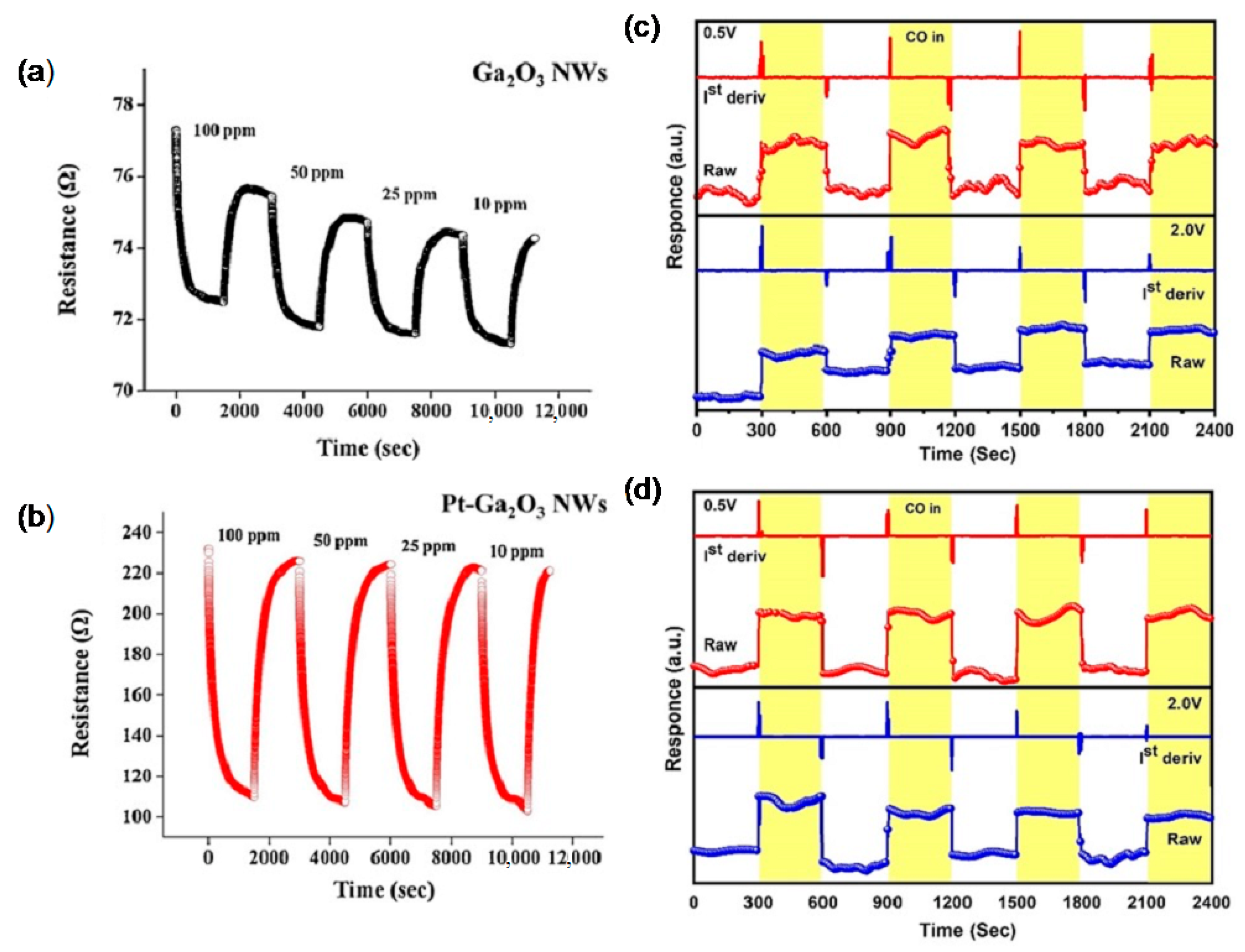
  124. Kim, H.; Jin, C.; An, S.; Lee, C. Fabrication and CO gas-sensing properties of Pt-functionalized Ga2O3 nanowires. Ceram. Int. 2012, 38, 3563–3567. [Google Scholar] [CrossRef]
  125. Park, S.; Kim, H.; Jin, C.; Lee, C. Synthesis, structure, and room-temperature gas sensing of multiple-networked Pd-doped Ga2O3 nanowires. J. Korean Phys. Soc. 2012, 60, 1560–1564. [Google Scholar] [CrossRef]
  126. Jin, C.; Park, S.; Kim, H.; Lee, C. Ultrasensitive multiple networked Ga2O3-core/ZnO-shell nanorod gas sensors. Sens. Actuators B Chem. 2012, 161, 223–228. [Google Scholar] [CrossRef]
  127. Tsai, T.-Y.; Chang, S.-J.; Weng, W.-Y.; Liu, S.; Hsu, C.-L.; Hsueh, H.-T.; Hsueh, T.-J. β-Ga2O3 nanowires-based humidity sensors prepared on GaN/sapphire substrate. IEEE Sens. J. 2013, 13, 4891–4896. [Google Scholar] [CrossRef]
  128. An, S.; Park, S.; Mun, Y.; Lee, C. UV enhanced NO2 sensing properties of Pt functionalized Ga2O3 nanorods. Bull. Korean Chem. Soc. 2013, 34, 1632–1636. [Google Scholar] [CrossRef] [Green Version]
  129. Park, S.H.; Kim, S.H.; Park, S.Y.; Lee, C. Synthesis and CO gas sensing properties of surface-nitridated Ga2O3 nanowires. RSC Adv. 2014, 4, 63402–63407. [Google Scholar] [CrossRef]
  130. Juan, Y.M.; Chang, S.-J.; Hsueh, H.T.; Wang, S.H.; Weng, W.Y.; Cheng, T.C.; Wu, C.L. Effects of humidity and ultraviolet characteristics on β-Ga2O3 nanowire sensor. RSC Adv. 2015, 5, 84776–84781. [Google Scholar] [CrossRef]
  131. Bui, Q.C.; Largeau, L.; Morassi, M.; Jegenyes, N.; Mauguin, O.; Travers, L.; Lafosse, X.; Dupuis, C.; Harmand, J.-C.; Tchernycheva, M.; et al. GaN/Ga2O3 core/shell nanowires growth: Towards high response gas sensors. Appl. Sci. 2019, 9, 3528. [Google Scholar] [CrossRef] [Green Version]
  132. Abdullah, Q.N.; Ahmed, A.R.; Ali, A.M.; Yam, F.K.; Hassan, Z.; Bououdina, M. Novel SnO2-coated β-Ga2O3 nanostructures for room temperature hydrogen gas sensor. Int. J. Hydrogen Energy 2021, 46, 7000–7010. [Google Scholar] [CrossRef]
  133. Park, S.; Kim, S.; Sun, G.-J.; Lee, C. Synthesis, structure and ethanol sensing properties of Ga2O3-core/WO3-shell nanostructures. Thin Solid Films 2015, 591, 341–345. [Google Scholar] [CrossRef]
  134. Sprincean, V.; Caraman, M.; Spataru, T.; Fernandez, F.; Paladi, F. Influence of the air humidity on the electrical conductivity of the β-Ga2O3-GaS structure: Air humidity sensor. Appl. Phys. A 2022, 128, 303. [Google Scholar] [CrossRef]
  135. Girija, K.; Thirumalairajan, S.; Mastelaro, V.R.; Mangalaraj, D. Catalyst free vapor-solid deposition of morphologically different β-Ga2O3 nanostructure thin films for selective CO gas sensors at low temperature. Anal. Methods 2016, 8, 3224–3235. [Google Scholar] [CrossRef]
  136. Almaev, A.V.; Nikolaev, V.I.; Yakovlev, N.N.; Butenko, P.N.; Stepanov, S.I.; Pechnikov, A.I.; Scheglov, M.P.; Chernikov, E.V. Hydrogen sensors based on Pt/α-Ga2O3: Sn/Pt structures. Sens. Actuators B Chem. 2022, 364, 131904. [Google Scholar] [CrossRef]
  137. Yakovlev, N.N.; Nikolaev, V.I.; Stepanov, S.I.; Almaev, A.V.; Pechnikov, A.I.; Chernikov, E.V.; Kushnarev, B.O. Effect of oxygen on the electrical conductivity of Pt-contacted α-Ga2O3/ε(κ)-Ga2O3 MSM structures on patterned sapphire substrates. IEEE Sens. J. 2021, 21, 14636–14644. [Google Scholar] [CrossRef]
  138. Krawczyk, M.; Korbutowicz, R.; Szukiewicz, R.; Wozniak, P.S.; Kuchowicz, M.; Teterycz, H. P-type inversion at the surface of β-Ga2O3 epitaxial layer modified with Au nanoparticles. Sensors 2022, 22, 932. [Google Scholar] [CrossRef]
  139. Liu, K.W.; Sakurai, M.; Aono, M. One-step fabrication of β-Ga2O3-amorphous-SnO2 core-shell microribbons and their thermally switchable humidity sensing properties. J. Mater. Chem. 2012, 22, 12882. [Google Scholar] [CrossRef]
  140. Weng, T.-F.; Ho, M.-S.; Sivakumar, C.; Balraj, B.; Chung, P.-F. VLS growth of pure and Au decorated β-Ga2O3 nanowires for room temperature CO gas sensor and resistive memory applications. Appl. Surf. Sci. 2020, 533, 147476. [Google Scholar] [CrossRef]
  141. Aymerich, E.L.; Gil, G.D.; Moreno, M.; Pellegrino, P.; Rodriguez, A.R. Fabrication, characterization and performance of low power gas sensors based on (GaxIn1-x)2O3 nanowires. Sensors 2021, 21, 3342. [Google Scholar] [CrossRef]
  142. Ge, X.T.; Fang, D.R.; Liu, X.Q. The preparation and gas-sensing properties of Ga2O3-NiO complex oxide by sol-gel method. Acta Phys. Chim. Sin. 2005, 21, 10–15. [Google Scholar] [CrossRef]
  143. Mohammadi, M.R.; Fray, D.J. Semiconductor TiO2-Ga2O3 thin film gas sensors derived from particulate sol-gel route. Acta Mater. 2007, 55, 4455–4466. [Google Scholar] [CrossRef]
  144. Mohammadi, M.R.; Fray, D.J.; Ghorbani, M. Comparison of single and binary oxide sol-gel gas sensors based on titania. Solid State Sci. 2008, 10, 884–893. [Google Scholar] [CrossRef]
  145. Hou, Y.; Jayatissa, A.H. Low resistive gallium doped nanocrystalline zinc oxide for gas sensor application via sol-gel process. Sens. Actuators B Chem. 2014, 204, 310–318. [Google Scholar] [CrossRef]
  146. Trinchi, A.; Galatsis, K.; Wlodarski, W.; Li, Y.X. A Pt/Ga2O3-ZnO/SiC Schottky diode-based hydrocarbon gas sensor. IEEE Sens. J. 2003, 3, 548–553. [Google Scholar] [CrossRef]
  147. Trinchi, A.; Li, Y.X.; Wlodarski, W.; Kaciulis, S.; Pandolfi, L.; Russo, S.P.; Duplessis, J.; Viticoli, S. Investigation of sol-gel prepared Ga-Zn oxide thin films for oxygen gas sensing. Sens. Actuators A Phys. 2003, 108, 263–270. [Google Scholar] [CrossRef]
  148. Li, Y.X.; Trinchi, A.; Wlodarski, W.; Galatsis, K.; Kalantar-zadeh, K. Investigation of the oxygen gas sensing performance of Ga2O3 thin films with different dopants. Sens. Actuators B Chem. 2003, 93, 431–434. [Google Scholar] [CrossRef]
  149. Trinchi, A.; Kaciulis, S.; Pandolfi, L.; Ghantasala, M.K.; Li, Y.X.; Wlodarski, W.; Viticoli, S.; Comini, E.; Sberveglieri, G. Characterization of Ga2O3 based MRISiC hydrogen gas sensors. Sens. Actuators B Chem. 2004, 103, 129–135. [Google Scholar] [CrossRef]
  150. Trinchi, A.; Wlodarski, W.; Li, Y.X. Hydrogen sensitive Ga2O3 Schottky diode sensor based on SiC. Sens. Actuators B Chem. 2004, 100, 94–98. [Google Scholar] [CrossRef]
  151. Trinchi, A.; Wlodarski, W.; Faglia, G.; Ponzoni, A.; Comini, E.; Sberveglieri, G. High temperature hydrocarbon sensing with Pt-thin Ga2O3-SiC diodes. Mater. Sci. Forum 2005, 483–485, 1033–1036. [Google Scholar] [CrossRef]
  152. Trinchi, A.; Wlodarski, W.; Li, Y.X.; Faglia, G.; Sberveglieri, G. Pt/Ga2O3/SiC MRISiC devices: A study of the hydrogen response. J. Phys. D Appl. Phys. 2005, 38, 754–763. [Google Scholar] [CrossRef]
  153. Bagheri, M.; Khodadadi, A.A.; Mahjoub, A.R.; Mortazavi, Y. Strong effects of gallia on structure and selective responses of Ga2O3-In2O3 nanocomposite sensors to either ethanol, CO or CH4. Sens. Actuators B Chem. 2015, 220, 590–599. [Google Scholar] [CrossRef]
  154. Lin, H.-J.; Baltrus, J.P.; Gao, H.; Ding, Y.; Nam, C.-Y.; Ohodnicki, P.; Gao, P.-X. Perovskite nanoparticle-sensitized Ga2O3 nanorod arrays for CO detection at high temperature. ACS Appl. Mater. Interfaces 2016, 8, 8880–8887. [Google Scholar] [CrossRef] [PubMed]
  155. Lin, H.-J.; Gao, H.; Gao, P.-X. UV-enhanced CO sensing using Ga2O3-based nanorod arrays at elevated temperature. Appl. Phys. Lett. 2017, 110, 043101. [Google Scholar] [CrossRef]
  156. Chen, H.; Hu, J.B.; Li, G.-D.; Gao, Q.; Wei, C.D.; Zou, X.X. Porous Ga-In bimetallic oxide nanofibers with controllable structures for ultrasensitive and selective detection of formaldehyde. ACS Appl. Mater. Interfaces 2017, 9, 4692–4700. [Google Scholar] [CrossRef]
  157. Zhang, Y.L.; Jia, C.W.; Kong, Q.; Fan, N.Y.; Chen, G.; Guan, H.T.; Dong, C.J. ZnO-decorated In/Ga oxide nanotubes derived from bimetallic In/Ga MOFs for fast acetone detection with high sensitivity and selectivity. ACS Appl. Mater. Interfaces 2020, 12, 26161. [Google Scholar] [CrossRef]
  158. Pilliadugula, R.; Krishnan, N. Gas sensing performance of GaOOH and β-Ga2O3 synthesized by hydrothermal method: A comparison. Mater. Res. Express 2018, 6, 025027. [Google Scholar] [CrossRef]
  159. Pilliadugula, R.; Krishnan, N.G. Effect of pH dependent morphology on room temperature NH3 sensing performances of β-Ga2O3. Mater. Sci. Semicond. Process. 2020, 112, 105007. [Google Scholar] [CrossRef]
  160. Wang, J.; Jiang, S.S.; Liu, H.L.; Wang, S.H.; Pan, Q.J.; Yin, Y.D.; Zhang, G. P-type gas-sensing behavior of Ga2O3/Al2O3 nanocomposite with high sensitivity to NOx at room temperature. J. Alloys Compd. 2020, 814, 152284. [Google Scholar] [CrossRef]
  161. Zhang, B.; Lin, H.-J.; Gao, H.Y.; Lu, X.X.; Nam, C.-Y.; Gao, P.-X. Perovskite-sensitized β-Ga2O3 nanorod arrays for highly selective and sensitive NO2 detection at high temperature. J. Mater. Chem. A 2020, 8, 10845–10854. [Google Scholar] [CrossRef]
  162. Pilliadugula, R.; Gopalakrishnan, N. Room temperature ammonia sensing performances of pure and Sn doped β-Ga2O3. Mater. Sci. Semicond. Process. 2021, 135, 106086. [Google Scholar] [CrossRef]
  163. Demin, I.E.; Kozlov, A.G. In2O3-Ga2O3 thin films for ammonia sensors of petrochemical industry safety systems. AIP Conf. Proc. 2018, 2007, 050004. [Google Scholar] [CrossRef]
  164. Demin, I.E.; Kozlov, A.G. Selectivity of the gas sensor based on the 50% In2O3-50% Ga2O3 thin film in dynamic mode of operation. J. Phys. Conf. Ser. 2018, 944, 012027. [Google Scholar] [CrossRef]
  165. Demin, I.E. Increasing the selectivity of semiconductor gas sensors working at sinusoidal-varying temperature for machine industry safety systems. J. Phys. Conf. Ser. 2019, 1260, 032008. [Google Scholar] [CrossRef] [Green Version]
  166. Demin, I.E. Selection of methods for increasing gas selectivity on the example of a sensor system based on In2O3-Ga2O3 semiconductor films. J. Phys. Conf. Ser. 2019, 1210, 012032. [Google Scholar] [CrossRef]
  167. Demin, I.E. Reducing the energy consumption of semiconductor methane sensors for gas alarm systems. AIP Conf. Proc. 2019, 2141, 050020. [Google Scholar] [CrossRef]
  168. Wei, Z.H.; Akbari, M.K.; Hai, Z.Y.; Ramachandran, R.K.; Detavernier, C.; Verpoort, F.; Kats, E.; Xu, H.Y.; Hu, J.; Zhuiykov, S. Ultra-thin sub-10 nm Ga2O3-WO3 heterostructures developed by atomic layer deposition for sensitive and selective C2H5OH detection on ppm level. Sens. Actuators B Chem. 2019, 287, 147–156. [Google Scholar] [CrossRef]
  169. Jochum, W.; Penner, S.; Fottinger, K.; Kramer, R.; Rupprechter, G.; Klotzer, B. Hydrogen on polycrystalline β-Ga2O3: Surface chemisorption, defect formation, and reactivity. J. Catal. 2008, 256, 268–277. [Google Scholar] [CrossRef]
  170. Vorobyeva, N.; Rumyantseva, M.; Platonov, V.; Filatova, D.; Chizhov, A.; Marikutsa, A.; Bozhev, I.; Gaskov, A. Ga2O3 (Sn) oxides for high-temperature gas sensors. Nanomaterials 2021, 11, 2938. [Google Scholar] [CrossRef]
  171. Pandeeswari, R.; Jeyaprakash, B.G. High sensing response of β-Ga2O3 thin film towards ammonia vapours: Influencing factors at room temperature. Sens. Actuators B Chem. 2014, 195, 206–214. [Google Scholar] [CrossRef]
  172. Yan, J.-T.; Lee, C.-T. Improved detection sensitivity of Pt/β-Ga2O3/GaN hydrogen sensor diode. Sens. Actuators B Chem. 2009, 143, 192–197. [Google Scholar] [CrossRef]
  173. Lee, C.-T.; Yan, J.-T. Investigation of a metal-insulator-semiconductor Pt/mixed Al2O3 and Ga2O3 insulator/AlGaN hydrogen sensor. J. Electrochem. Soc. 2010, 157, J281. [Google Scholar] [CrossRef]
  174. Lee, C.-T.; Yan, J.-T. Sensing mechanisms of Pt/β-Ga2O3/GaN hydrogen sensor diodes. Sens. Actuators B Chem. 2010, 147, 723–729. [Google Scholar] [CrossRef]
  175. Shafiei, M.; Hoshyargar, F.; Motta, N.; O’Mullane, A.P. Utilizing p-type native oxide on liquid metal microdroplets for low temperature gas sensing. Mater. Des. 2017, 122, 288–295. [Google Scholar] [CrossRef] [Green Version]
  176. Saidi, S.A.; Tang, J.; Yang, J.; Han, J.; Daeneke, T.; O’Mullane, A.P.; Kalantar-Zadeh, K. Liquid metal-based route for synthesizing and tuning gas-sensing elements. ACS Sens. 2020, 5, 1177–1189. [Google Scholar] [CrossRef]
  177. Sivasankaran, B.R.; Balaji, M. Novel gallium oxide/reduced graphene oxide nanocomposite for ammonia gas sensing application. Mater. Lett. 2021, 288, 129386. [Google Scholar] [CrossRef]
  178. Ji, H.; Zeng, W.; Li, Y. Gas sensing mechanisms of metal oxide semiconductors: A focus review. Nanoscale 2019, 11, 22664–22684. [Google Scholar] [CrossRef]
  179. Fleischer, M.; Meixner, H. Fast gas sensors based on metal oxides which are stable at high temperatures. Sens. Actuators B Chem. 1997, 43, 1–10. [Google Scholar] [CrossRef]
  180. Fleischer, M.; Meixner, H. Thin-film gas sensors based on high-temperature-operated metal oxides. J. Vac. Sci. Technol. A 1999, 17, 1866–1872. [Google Scholar] [CrossRef]
  181. Hoefer, U.; Frank, J.; Fleischer, M. High temperature Ga2O3-gas sensors and SnO2-gas sensors: A comparison. Sens. Actuators B Chem. 2001, 78, 6–11. [Google Scholar] [CrossRef]
  182. Fleischer, M. Advances in application potential of adsorptive-type solid state gas sensors: High-temperature semiconducting oxides and ambient temperature GasFET devices. Meas. Sci. Technol. 2008, 19, 042001. [Google Scholar] [CrossRef]
  183. Pohle, R.; Weisbrod, E.; Hedler, H. Enhancement of MEMS-based Ga2O3 gas sensors by surface modifications. Proc. Eng. 2016, 168, 211–215. [Google Scholar] [CrossRef]
  184. Weisz, P.B.; Prater, C.D. Interpretation of measurements in experimental catalysis. Adv. Catal. 1954, 6, 143. [Google Scholar] [CrossRef]
  185. Jaaniso, R.; Tan, O.K. Semiconductor Gas Sensors; Woodhead Publishing: Duxford, UK, 2019; pp. 27–34. [Google Scholar] [CrossRef]
  186. Yamazoe, N. New approaches for improving semiconductor gas sensors. Sens. Actuators B Chem. 1991, 5, 7–19. [Google Scholar] [CrossRef]
  187. Korotcenkov, G. Handbook of Gas Sensor Materials; Springer: New York, NY, USA, 2013; pp. 49–116. [Google Scholar] [CrossRef]
  188. Frank, J.; Fleischer, M.; Meixner, H. Gas-sensitive electrical properties of pure and doped semiconducting Ga2O3 thick films. Sens. Actuators B Chem. 1998, 48, 318–321. [Google Scholar] [CrossRef]
  189. Frank, J.; Fleischer, M.; Meixner, H.; Feltz, A. Enhancement of sensitivity and conductivity of semiconducting Ga2O3 gas sensors by doping with SnO2. Sens. Actuators B Chem. 1998, 49, 110–114. [Google Scholar] [CrossRef]
  190. Schwebel, T.; Fleischer, M.; Meixner, H. A selective, temperature compensated O2 sensor based on Ga2O3 thin films. Sens. Actuators B Chem. 2000, 65, 176–180. [Google Scholar] [CrossRef]
  191. Fleischer, M.; Meixner, H. Sensing reducing gases at high temperatures using long-term stable Ga2O3 thin films. Sens. Actuators B Chem. 1992, 6, 257–261. [Google Scholar] [CrossRef]
  192. Hacker, B.; Fleischer, M.; Meixner, H. Topography and performance of gas-sensing devices: An AFM study. Scanning 1993, 15, 291–294. [Google Scholar] [CrossRef]
  193. Weh, T.; Fleischer, M.; Meixner, H. Optimization of physical filtering for selective high temperature H2 sensors. Sens. Actuators B Chem. 2000, 68, 146–150. [Google Scholar] [CrossRef]
  194. Weh, T.; Frank, J.; Fleischer, M.; Meixner, H. On the mechanism of hydrogen sensing with SiO2 modificated high temperature Ga2O3 sensors. Sens. Actuators B Chem. 2001, 78, 202–207. [Google Scholar] [CrossRef]
  195. Wiesner, K.; Knozinger, H.; Fleischer, M.; Meixner, H. Working mechanism of an ethanol filter for selective high-temperature methane gas sensors. IEEE Sens. J. 2002, 2, 354–359. [Google Scholar] [CrossRef]
  196. Biskupski, D.; Geupel, A.; Wiesner, K.; Fleischer, M.; Moos, R. Platform for a hydrocarbon exhaust gas sensor utilizing a pumping cell and a conductometric sensor. Sensors 2009, 9, 7498–7508. [Google Scholar] [CrossRef] [PubMed] [Green Version]
  197. Giber, J.; Perczel, I.V.; Gerblinger, J.; Lampe, U.; Fleischer, M. Coadsorption and cross sensitivity on high temperature semiconducting metal oxides: Water effect on the coadsorption process. Sens. Actuators B Chem. 1994, 18–19, 113–118. [Google Scholar] [CrossRef]
  198. Reti, F.; Fleischer, M.; Meixner, H.; Giber, J. Effect of coadsorption of reducing gases on the conductivity of β-Ga2O3 thin films in the presence of O2. Sens. Actuators B Chem. 1995, 18–19, 573–577. [Google Scholar] [CrossRef]
  199. Reti, F.; Fleischer, M.; Meixner, H.; Giber, J. Influence of water on the coadsorption of oxidizing and reducing gases on the β-Ga2O3 surface. Sens. Actuators B Chem. 1994, 18, 138–142. [Google Scholar] [CrossRef]
  200. Reti, F.; Fleischer, M.; Gerblinger, J.; Lampe, U.; Varhegyi, E.B.; Perczel, V.; Meixner, H.; Giber, J. Comparison of the water effect on the resistance of different semiconducting metal oxides. Sens. Actuators B Chem. 1995, 26–27, 103–107. [Google Scholar] [CrossRef]
  201. Pohle, R.; Fleischer, M.; Meixner, H. In situ infrared emission spectroscopic study of the adsorption of H2O and hydrogen-containing gases on Ga2O3 gas sensors. Sens. Actuators B Chem. 2000, 68, 151–156. [Google Scholar] [CrossRef]
  202. Varhegyi, E.B.; Perczel, I.V.; Gerblinger, J.; Fleischer, M.; Meixner, H.; Giber, J. Auger and SIMS study of segregation and corrosion some semiconducting oxide gas-sensor materials. Sens. Actuators B Chem. 1994, 18–19, 569–572. [Google Scholar] [CrossRef]
  203. Hovhannisyan, R.V.; Khondkaryan, H.D.; Aleksanyan, M.S.; Arakelyan, V.M.; Semerjyan, B.O.; Gasparyan, F.V.; Aroutiounian, V.M. Static and noise characteristics of nanocomposite gas sensors. J. Contemp. Phys. 2014, 49, 151–157. [Google Scholar] [CrossRef]
  204. Dyndal, K.; Zarzycki, A.; Andrysiewicz, W.; Grochala, D.; Marszalek, K.; Rydosz, A. CuO-Ga2O3 thin films as a gas-sensitive material for acetone detection. Sensors 2020, 20, 3142. [Google Scholar] [CrossRef]
  205. Lundstrom, I.; Shivaraman, S.; Svensson, C.; Lundkvist, L. A hydrogen-sensitive MOS field-effect transistor. Appl. Phys. Lett. 1975, 26, 55–57. [Google Scholar] [CrossRef]
  206. Leu, M.; Doll, T.; Flietner, B.; Lechner, J.; Eisele, I. Evaluation of gas mixtures with different sensitive layers incorporated in hybrid FET structures. Sens. Actuators B Chem. 1994, 18–19, 678–681. [Google Scholar] [CrossRef]
  207. Geistlinger, H. Accumulation layer model for Ga2O3 thin-film gas sensors based on the Volkenstein theory of catalysis. Sens. Actuators B Chem. 1994, 18, 125–131. [Google Scholar] [CrossRef]
  208. Geistlinger, H.; Eisele, I.; Flietner, B.; Winter, R. Dipole- and charge transfer contributions to the work function change of semiconducting thin films: Experiment and theory. Sens. Actuators B Chem. 1996, 34, 499–505. [Google Scholar] [CrossRef]
  209. Shin, W.; Hong, S.; Jeong, Y.; Jung, G.; Park, J.; Kim, D.; Park, B.-G.; Lee, J.-H. Effects of channel length scaling on the signal-to-noise ratio in FET-type gas sensor with horizontal floating-gate. IEEE Electron Device Lett. 2022, 43, 442–445. [Google Scholar] [CrossRef]
  210. Imanaka, N.; Tamura, S.; Adachi, G. Ammonia sensor based on ionically exchanged NH4+-gallate solid electrolytes. Electrochem. Solid State Lett. 1999, 1, 282. [Google Scholar] [CrossRef]
  211. Westphal, D.; Jakobs, S.; Guth, U. Gold-composite electrodes for hydrocarbon sensors based on YSZ solid electrolyte. Ionics 2001, 7, 182–186. [Google Scholar] [CrossRef]
  212. Zosel, J.; Westphal, D.; Jakobs, S.; Muller, R.; Guth, U. Au-oxide composites as HC-sensitive electrode material for mixed potential gas sensors. Solid State Ion. 2002, 152–153, 525. [Google Scholar] [CrossRef]
  213. Zosel, J.; Ahlborn, K.; Muller, R.; Westphal, D.; Vashook, V.; Guth, U. Selectivity of HC-sensitive electrode materials for mixed potential gas sensors. Solid State Ion. 2002, 169, 115–119. [Google Scholar] [CrossRef]
  214. Zhang, W.-F.; Schmidt-Zhang, P.; Guth, U. Electrochemical studies on cells M/YSZ/Pt (M = Pt, Pt-Ga2O3) in NO, O2, N2 gas mixtures. Solid State Ion. 2004, 169, 121–128. [Google Scholar] [CrossRef]
  215. Shuk, P.; Bailey, E.; Zosel, J.; Guth, U. New advanced in situ carbon monoxide sensor for the process application. Ionics 2009, 15, 131–138. [Google Scholar] [CrossRef]
  216. Wu, N.Q.; Chen, Z.; Xu, J.H.; Chyu, M.; Mao, S.X. Impedance-metric Pt/YSZ/Au-Ga2O3 sensor for CO detection at high temperature. Sens. Actuators B Chem. 2005, 110, 49–53. [Google Scholar] [CrossRef]
  217. Yan, S.C.; Wan, L.J.; Li, Z.S.; Zhou, Y.; Zou, Z.G. Synthesis of a mesoporous single crystal Ga2O3 nanoplate with improved photoluminescence and high sensitivity in detecting CO. Chem. Commun. 2010, 46, 6388. [Google Scholar] [CrossRef]
  218. Korotcenkov, G.; Han, S.H.; Cho, B.K. Material design for metal oxide chemiresistive gas sensors. J. Sens. Sci. Technol. 2013, 22, 1–17. [Google Scholar] [CrossRef] [Green Version]
  219. Bartic, M.; Ogita, M.; Isai, M.; Baban, C.; Suzuki, H. Oxygen sensing properties at high temperatures of β-Ga2O3 thin films deposited by the chemical solution deposition method. J. Appl. Phys. 2007, 102, 023709. [Google Scholar] [CrossRef]
  220. Wang, D.; Lou, Y.L.; Wang, R.; Wang, P.P.; Zheng, X.J.; Zhang, Y.; Jiang, N. Humidity sensor based on Ga2O3 nanorods doped with Na+ and K+ from GaN powder. Ceram. Int. 2015, 41, 14790–14797. [Google Scholar] [CrossRef]
  221. Potje-Kamloth, K. Semiconductor junction gas sensors. Chem. Rev. 2008, 108, 367–399. [Google Scholar] [CrossRef]
  222. Ratko, A.; Babushkin, O.; Baran, A.; Baran, S. Sorption and gas sensitive properties of In2O3 based ceramics doped with Ga2O3. J. Eur. Ceram. Soc. 1998, 18, 2227–2232. [Google Scholar] [CrossRef]
  223. Silver, A.T.; Juarez, A.S. SnO2: Ga thin films as oxygen gas sensor. Mater. Sci. Eng. B 2004, 110, 268–271. [Google Scholar] [CrossRef]
  224. Bagheri, M.; Khodadadi, A.A.; Mahjoub, A.R.; Mortazavi, Y. Highly sensitive gallia-SnO2 nanocomposite sensors to CO and ethanol in presence of methane. Sens. Actuators B Chem. 2013, 188, 45–52. [Google Scholar] [CrossRef]
  225. Du, L.T.; Li, H.Y.; Li, S.; Liu, L.; Li, Y.; Xu, S.Y.; Gong, Y.M.; Cheng, Y.L.; Zeng, X.G.; Liang, Q.C. A gas sensor based on Ga-doped SnO2 porous microflowers for detecting formaldehyde at low temperature. Chem. Phys. Lett. 2018, 713, 235–241. [Google Scholar] [CrossRef]
  226. Kevin, M.; Tho, W.H.; Ho, G.W. Transferability of solution processed epitaxial Ga:ZnO films; tailored for gas sensor and transparent conducting oxide applications. J. Mater. Chem. 2012, 22, 16442. [Google Scholar] [CrossRef]
  227. Vorobyeva, N.; Rumyantseva, M.; Filatova, D.; Konstantinova, E.; Grishina, D.; Abakumov, A.; Turner, S.; Gaskov, A. Nanocrystalline ZnO(Ga): Paramagnetic centers, surface acidity and gas sensor properties. Sens. Actuators B Chem. 2013, 182, 555–564. [Google Scholar] [CrossRef]
  228. Rashid, T.-R.; Phan, D.-T.; Chung, G.-S. Effect of Ga-modified layer on flexible hydrogen sensor using ZnO nanorods decorated by Pd catalysts. Sens. Actuators B Chem. 2014, 193, 869–876. [Google Scholar] [CrossRef]
  229. Girija, K.G.; Somasundaram, K.; Debnath, A.K.; Topkar, A.; Vatsa, R.K. Enhanced H2S sensing properties of gallium doped ZnO nanocrystalline films as investigated by DC conductivity and impedance spectroscopy. Mater. Chem. Phys. 2018, 214, 297–305. [Google Scholar] [CrossRef]
  230. Fleischer, M.; Meixner, H. Selectivity in high-temperature operated semiconductor gas-sensors. Sens. Actuators B Chem. 1998, 52, 179–187. [Google Scholar] [CrossRef]
  231. Anichini, C.; Czepa, W.; Pakulski, D.; Aliprandi, A.; Ciesielski, A.; Samori, P. Chemical sensing with 2D materials. Chem. Soc. Rev. 2018, 47, 4860–4908. [Google Scholar] [CrossRef] [Green Version]
  232. Zhao, J.L.; Huang, X.R.; Yin, Y.H.; Liao, Y.K.; Mo, H.W.; Qian, Q.K.; Guo, Y.Z.; Chen, X.L.; Zhang, Z.F.; Hua, M.Y. Two-dimensional gallium oxide monolayer for gas-sensing application. J. Phys. Chem. Lett. 2021, 12, 5813–5820. [Google Scholar] [CrossRef]
  233. Wang, S.; Li, H.; Huang, H.; Cao, X.; Chen, X.; Cao, D. Porous organic polymers as a platform for sensing applications. Chem. Soc. Rev. 2022, 51, 2031–2080. [Google Scholar] [CrossRef]
  234. Yang, Y.; Zhang, P. Dissociation of H2 molecule on the β-Ga2O3 (100)B surface: The critical role of oxygen vacancy. Phys. Lett. A 2010, 374, 4169–4173. [Google Scholar] [CrossRef] [Green Version]
  235. Nagarajan, V.; Chandiramouli, R. Methane adsorption characteristics on β-Ga2O3 nanostructures: DFT investigation. Appl. Surf. Sci. 2015, 344, 65–78. [Google Scholar] [CrossRef]
  236. Yaqoob, U.; Younis, M.I. Chemical gas Sensors: Recent developments, challenges, and the potential of machine Learning—A review. Sensors 2021, 21, 2877. [Google Scholar] [CrossRef] [PubMed]
  237. Mohmed, M.; Attia, N.; Elashery, S. Greener and facile synthesis of hybrid nanocomposite for ultrasensitive iron (II) detection using carbon sensor. Microporous Mesoporous Mater. 2021, 313, 110832. [Google Scholar] [CrossRef]
  238. Elashery, S.; Attia, N.; Oh, H. Design and fabrication of novel flexible sensor based on 2D Ni-MOF nanosheets as a preliminary step toward wearable sensor for onsite Ni (II) ions detection in biological and environmental samples. Anal. Chim. Acta 2022, 1197, 339518. [Google Scholar] [CrossRef] [PubMed]
  239. Rahman, T.; Masui, T.; Ichiki, T. Single-crystal gallium oxide-based biomolecular modified diode for nucleic acid sensing. Jpn. J. Appl. Phys. 2015, 54, 04DL08. [Google Scholar] [CrossRef]
  240. Das, M.; Chakraborty, T.; Lin, C.H.; Lin, R.; Kao, C.H. Screen-printed Ga2O3 thin film derived from liquid metal employed in highly sensitive pH and non-enzymatic glucose recognition. Mater. Chem. Phys. 2022, 278, 125652. [Google Scholar] [CrossRef]
Figure 1. Number of publications on Ga2O3-based gas sensors from 1990 to 2022. Data extracted from Web of Science with keywords “sensor” or “sensing” and “Ga2O3” or “gallium oxide”.
Materials 15 07339 g001
Figure 2. Interconversion relation of Ga2O3 polymorphs [22]. Copyright 2019 Elsevier.
Materials 15 07339 g002
Figure 3. (a) Crystal structures of six polymorphs of Ga2O3. (b) The (001), (010), and ( 2 ¯ 01) planes for β-Ga2O3. Original drawing using VESTA was done by us.
Materials 15 07339 g003
Figure 4. (a) The Hall mobility and (b) electron density as functions as the temperature for β-Ga2O3 single crystals grown by the Czochralski method [58]. Copyright 2011 American Institute of Physics. (c) The Hall mobility and (d) electron density as functions as the temperature for Si-doped homoepitaxial films grown on β-Ga2O3 (001) substrate by halide vapor-phase epitaxy [60]. Copyright 2018 Elsevier. (e) The Hall mobility and (f) electron density as functions as the temperature for silicon-doped β-Ga2O3 homoepitaxial films grown on β-Ga2O3 (010)-oriented substrates via metalorganic chemical vapor deposition [56]. Copyright 2019 American Institute of Physics.
Materials 15 07339 g004
Figure 5. (a) AFM images of the Cr-doped Ga2O3 sputtering thin film [87]. XRD patterns of (b) pure Ga2O3 thin films and (c) Cr-doped Ga2O3 thin films [87]. Copyright 2020 Elsevier.
Materials 15 07339 g005
Figure 7. (a) SEM images of the morphological evolution of β-Ga2O3 nanostructures [159]. (b) Schematic representation of morphological evolutions at different pH values [159]. Copyright 2020 Elsevier.
Materials 15 07339 g007
Figure 8. (a) The model of the three temperature-dependent regimes of the gas reaction of Ga2O3 [182]. Copyright 2008 IOP. (b) The model and corresponding energy diagram of Ga2O3 grain contact [87]. Copyright 2020 Elsevier.
Materials 15 07339 g008
Figure 9. Schematic device structures for (a) resistor-type (b) SBD-type, (c) FET-type, and (d) capacitor-type Ga2O3-based gas sensors. Redrawn with permission from G. Korotcenkov [187]. Copyright 2014 Springer.
Materials 15 07339 g009
Figure 10. Schematic device structures for electrochemical gas sensors: (a) NH4+-Ga2O3 solid electrolyte [210] Copyright 1998 The Electrochemical Society. (b) YSZ solid electrolyte [214]. Copyright 2004 Elsevier.
Materials 15 07339 g010
Figure 11. Nitrogen adsorption-desorption isotherm of the Ga2O3 (a) rectangular and (b) rod-shaped nanostructures (inset: the corresponding pore size distribution). Sensing response and electrical resistance as a function of CO concentration at 100 °C (c) β-Ga2O3 rectangular nanorods, (d) β-Ga2O3 nanorods, (e) response time, and (f) recovery time of different β-Ga2O3 nanostructure thin films [135]. Copyright 2016 The Royal Society of Chemistry.
Materials 15 07339 g011
Figure 12. Gas responses of (a) bare Ga2O3 nanowires and (b) Pt-coated Ga2O3 nanowires to 10, 25, 50, and 100 ppm CO gas at 100 °C [124]. Copyright 2012 Elsevier. Room temperature CO gas sensor measurement results with different bias voltages for (c) pure β-Ga2O3 nanowires and (d) Au-decorated β-Ga2O3 nanowire with 2158 ppm CO concentration [140]. Copyright 2020 Elsevier.
Materials 15 07339 g012
Figure 13. Enhancement of the sensitivity to (a) 1% CO and (b) 1% CH4 of Sn-doped Ga2O3 thin films compared to undoped films [189]. Copyright 1998 Elsevier. (c) Sensor signal as a function of NH3 concentration for Sn-doped Ga2O3 samples measured at 500 °C [170]. Copyright 2021 MDPI. (d) Room temperature-sensing response as a function of NH3 concentration [162]. Copyright 2021 Elsevier.
Materials 15 07339 g013
Figure 14. Schematic illustrations of the energy band structures at heterojunction interfaces of (a) p–n and (b) n–n of heterojunctions [178]. 2019 The Royal Society of Chemistry.
Materials 15 07339 g014
Figure 15. (a) TEM image of a β-Ga2O3 nanorod coated with 5 nm LSFO. (b) Sensitivity, (c) response time, and (d) recover time of gas sensors made by β-Ga2O3/LSFO nanorods upon exposure to CO at 500 °C [154]. Copyright 2016 American Chemical Society. (e) TEM image of a β-Ga2O3 nanorod coated with 8 nm LSCO. (f) Sensitivity, (g) response time, and (h) recover time of gas sensors made by β-Ga2O3/LSCO nanorods upon exposure to NO2 at 800 °C [161]. Copyright 2020 The Royal Society of Chemistry.
Materials 15 07339 g015
Figure 16. (a) H2S Response of Ga-doped ZnO gas sensors as a function of the gas concentration [227]. Copyright 2013 Elsevier. (b) H2S Response of Ga-doped ZnO gas sensors as a function of the temperature [229]. Copyright 2018 Elsevier.
Materials 15 07339 g016
Figure 17. Conceptual diagrams for physical and chemical filters of Ga2O3-based gas sensors [230]. Copyright 1998 Elsevier.
Materials 15 07339 g017
Figure 18. Schematics and energy-level representations of the β-Ga2O3 nanowires (a) before and (b) after the 254 nm UV illumination [107]. Copyright 2006 American Institute of Physics.
Materials 15 07339 g018
Figure 19. CO gas-sensing performance comparison of pristine, LSFO-decorated, and Pt-decorated β-Ga2O3 nanorod arrays: (a) normalized sensitivity time characteristics and (b) sensitivity, recovery time, and recovery time under dark or UV illumination tested at 500 °C [155]. Copyright 2017 American Institute of Physics. (c) Room temperature gas responses of Pt-functionalized Ga2O3 nanorod gas sensors to 5 ppm NO2 under UV light illumination with varied intensities [128]. Copyright 2013 Korean Chemical Society.
Materials 15 07339 g019
Figure 20. Radar chart of seven performance enhancement strategies of gas sensors made by Ga2O3 bulk crystal, thin films, and nanostructures. Original drawing was done by us.
Materials 15 07339 g020
Table 1. Basic properties of Ga2O3 polymorphs [22,32].
PolymorphSystemSpace GroupLattice Parameters
αhexagonal R 3 ¯ c a = b = 4.98–5.04 Å, c = 13.4–13.6 Å,
α = β = 90°, γ = 120°
βmonoclinicC2/ma = 12.12–12.34 Å, b = 3.03–3.04 Å, c = 5.80–5.87 Å,
α = β = 90°, γ = 103.8°
γcubic Fd 3 ¯ m a = b = c = 8.24–8.30 Å,
α = β = γ = 90°
δcubicIa3a = b = c = 9.40–10.1 Å,
α = β = γ = 90°
εhexagonalP63mca = 5.06–5.12 Å, b = 8.69–8.79 Å, c = 9.3–9.4 Å,
α = β = 90°, γ = 120°
κorthorhombicPna21a = 5.05 Å, b = 8.69 Å, c = 9.27 Å,
α = β = γ = 90°
Table 2. Basic electric properties of β-Ga2O3 [32,61].
Electric PropertiesValue
Electronic effective mass (m0)0.28
Static dielectric constant10
High frequency dielectric constant3.9
Electron mobility (cm2·V−1·s−1)200
Range of free electron concentration (cm−3)1016~1020
Range of doping concentration (cm−3)1017~1020
Electron affinity (eV)4.0
Break down field (eV/cm)8.0
Typical types of shallow donorsSn, Ge, Si
Table 3. Target gases of Ga2O3-based gas sensors.
Electrical Gas SensorsElectrochemical
Gas Sensor
Optical
Gas Sensor
ResistorSBDFETCapacitor
Environmental gasesO2, CO2, O3, NH3, SO2O2, NH3NH3 NH3
Highly toxic gasesCO, H2S, NO, NO2CO, NOCO, NO2 CO
Combustible gasesH2, CH4, C4H10, C3H8, C4H8, C7H8H2, CH4, C3H6H2C7H8C3H6
VOCsC2H6O, C3H6O, C3H8O C2H6O, C3H6O, C3H8O C2H6O, C3H6O, C3H8O
HumidityH2O
Other gasesC2H6S CH3NO2, C6H15N
Table 4. Enhanced sensing performances of gas sensors using Ga-contained metal oxides.
Sensing MaterialPreparationSensitivity @Gas ConcentrationOperating TemperatureResponse/Recover
Time (s)
Other ObservationsReference
Ga-doped In2O3
nanowire
CVD1.05 @ 80 ppm C2H6O20040/800 [141]
2.2 @ 4 ppm NO22001980/2780
Ga-doped In2O3
nanofiber
Hydrothermal synthesis52.5 @ 100 ppm CH2O1501/70The low limit
of detection is 0.2 ppm
[156]
Ga-doped In2O3
film
PLD2.15 @ 25 ppm NH3623 [164]
20.5 @ 25 ppm C2H6O504
24.4 @ 25 ppm C3H6O504
7.47 @ 25 ppm
CH4
500 [167]
Ga-doped In2O3
ceramics
Coprecipitation0.85 @ 0.5% CH4380 [222]
Ga-doped SnO2 filmSpray pyrolysis3.1 @ 1 Torr O2350 [223]
Ga-doped SnO2
nanocomposites
Coprecipitation315 @ 300 ppm CO30036 [224]
Ga-doped SnO2
nanocomposites
119 @ 300 ppm C2H6O25093
Ga-doped SnO2
microflowers
Hydrothermal synthesis95.8 @ 50 ppm CH2O2303The low limit
of detection is 0.1 ppm
[225]
Ga-doped ZnO
film
Sol–gel synthesis0.5 @ 500 ppm H2130475 [145]
Ga-doped ZnO
Nanorod
Hydrothermal synthesis1.01% @ 250 ppm C2H6ORT [226]
Ga-doped ZnO
nanoparticle
Spray pyrolysis56 @ 2 ppm NO2250 [227]
8 @ 1 ppm H2S250
Ga-doped ZnO
nanorod
Sol–gel synthesis0.91 @ 100 ppm H2RT20 [228]
Ga-doped ZnO
film
Magnetron sputtering2.4 @ 5 ppm
H2S
300 [229]
  S = R a R g / Ra ; S = R a / R g ; S = R a R g / R g
Publisher’s Note: MDPI stays neutral with regard to jurisdictional claims in published maps and institutional affiliations.

