
Study of the Layer-Type BST Thin Film with X-ray Diffraction and X-ray Photoelectron Spectroscopy


Abstract
:1. Introduction
2. Materials and Methods
3. Results and Discussion
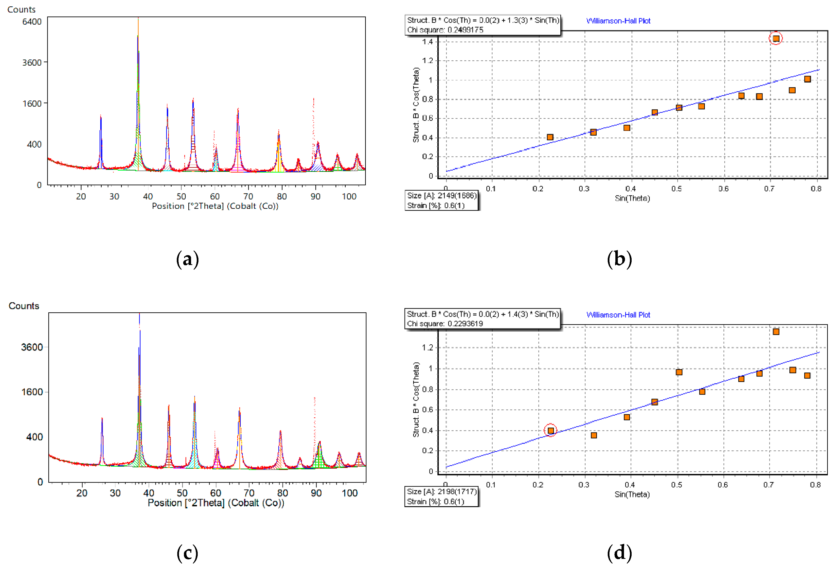
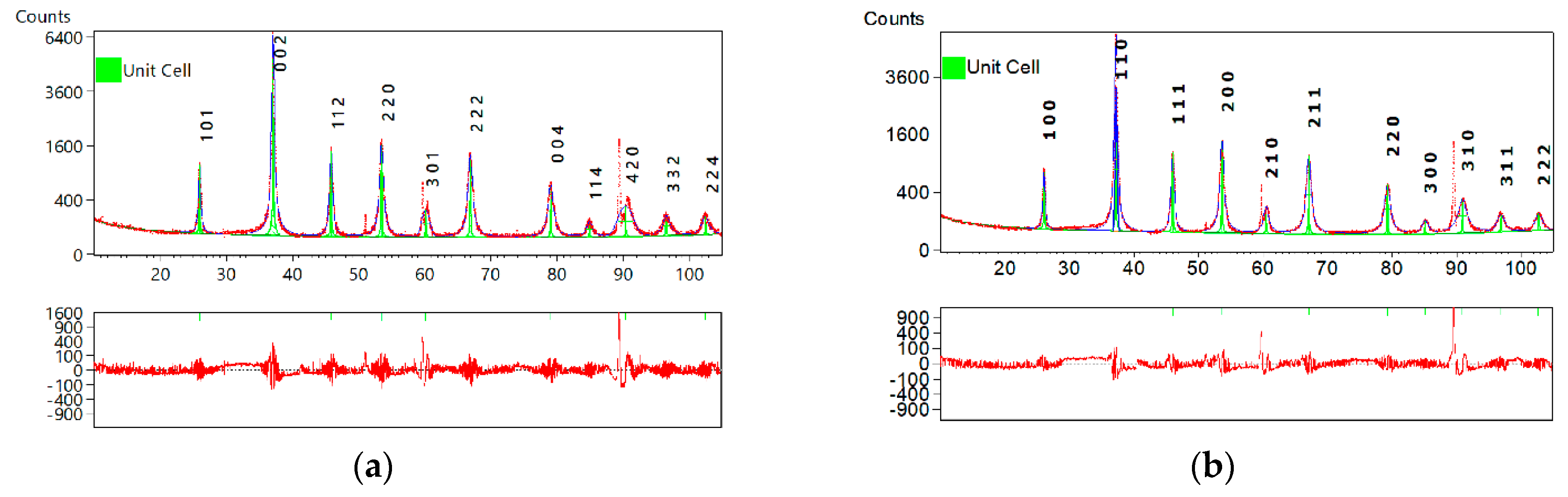
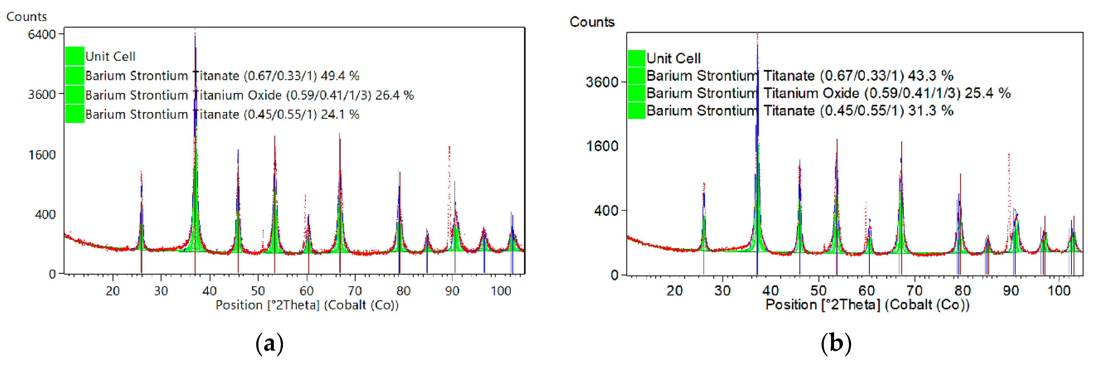
3.1. Crystal Structure of BST Ceramic Thin Film
- Barium Strontium Titanate, chemical formula: Ba0.67O3Sr0.33Ti1-tetragonal, space group: P4mm(99), ICSD collection code: 54150, PDF number (calculated powder diffraction data) 01-089-0274.
- Barium Strontium Titanium Oxide, chemical formula: Ba0.592O3Sr0.408Ti1-cubic, space group: Pm-3m(221), ICSD collection code: 90006, PDF number (calculated powder diffraction data): 01-070-3628.
- Barium Strontium Titanate, chemical formula: Ba0.45O3Sr0.55Ti1-cubic, space group: Pm-3m(221), ICSD collection code: 154403, PDF code: 00-039-1395.
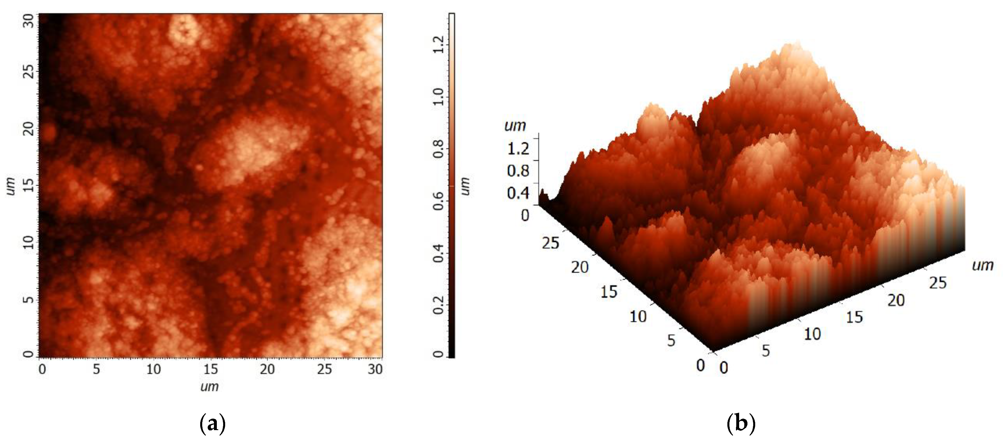
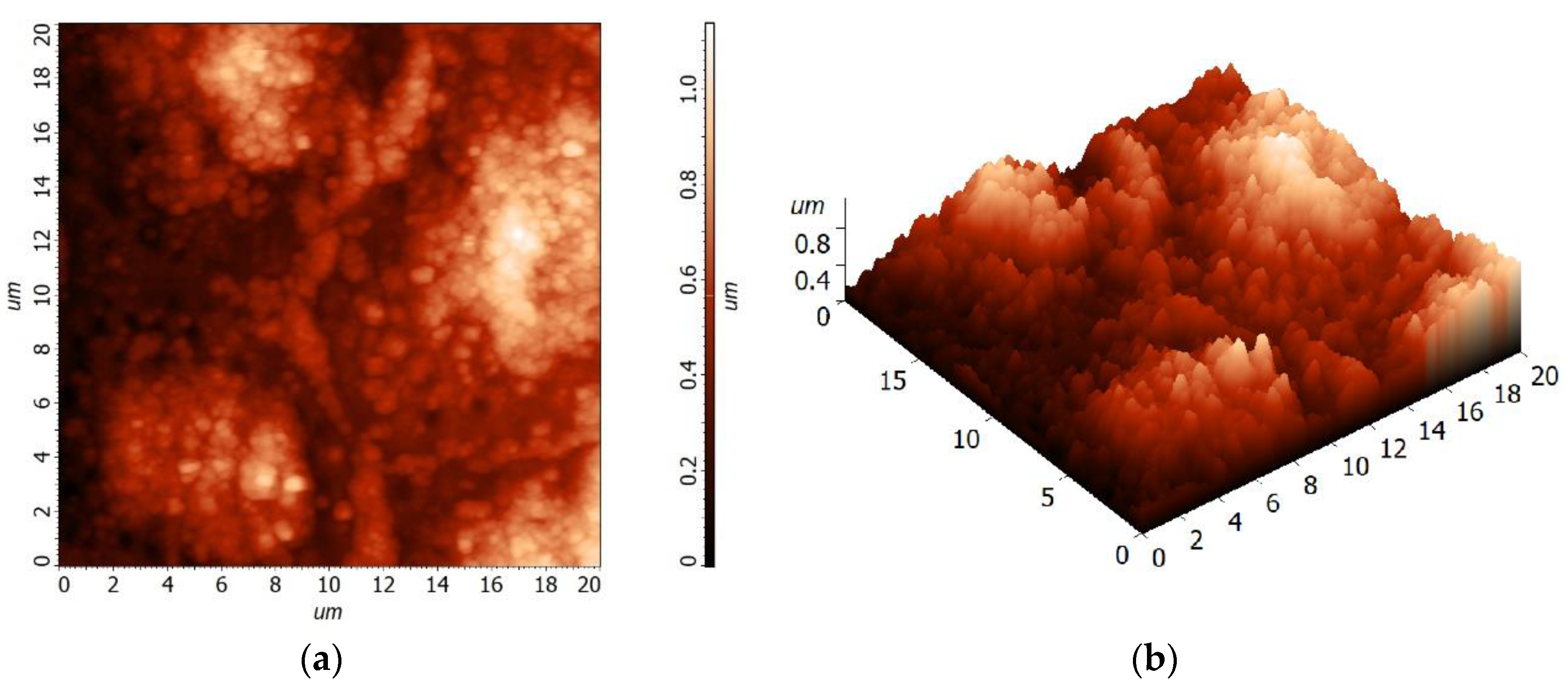
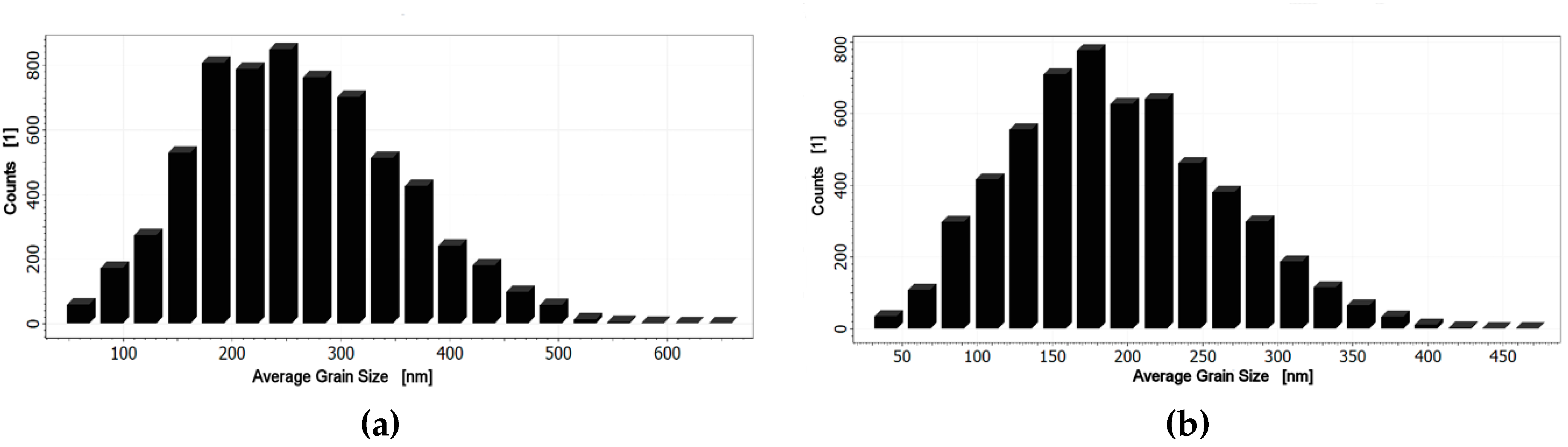
3.2. Morphology Studies of the Thin Film
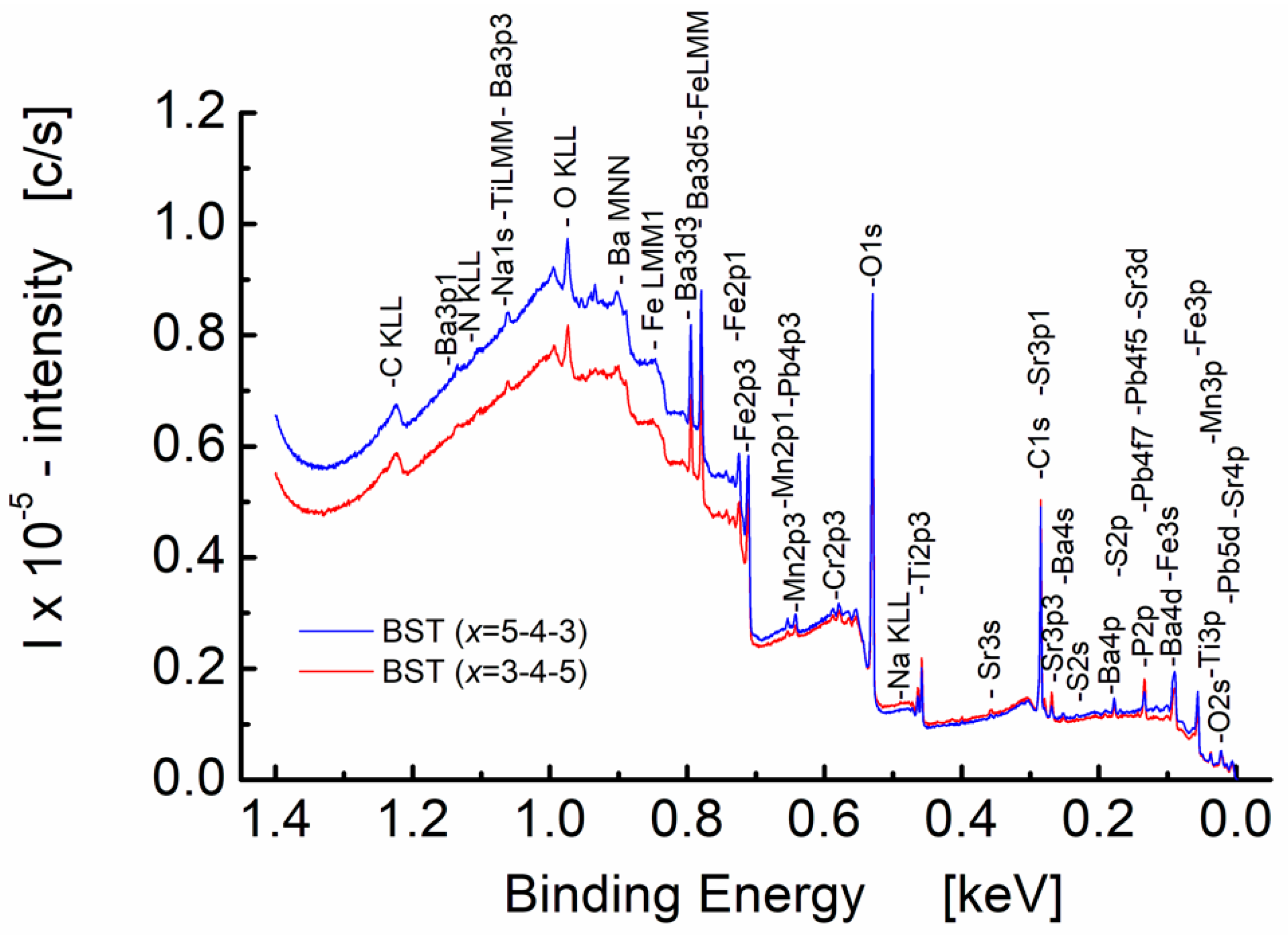
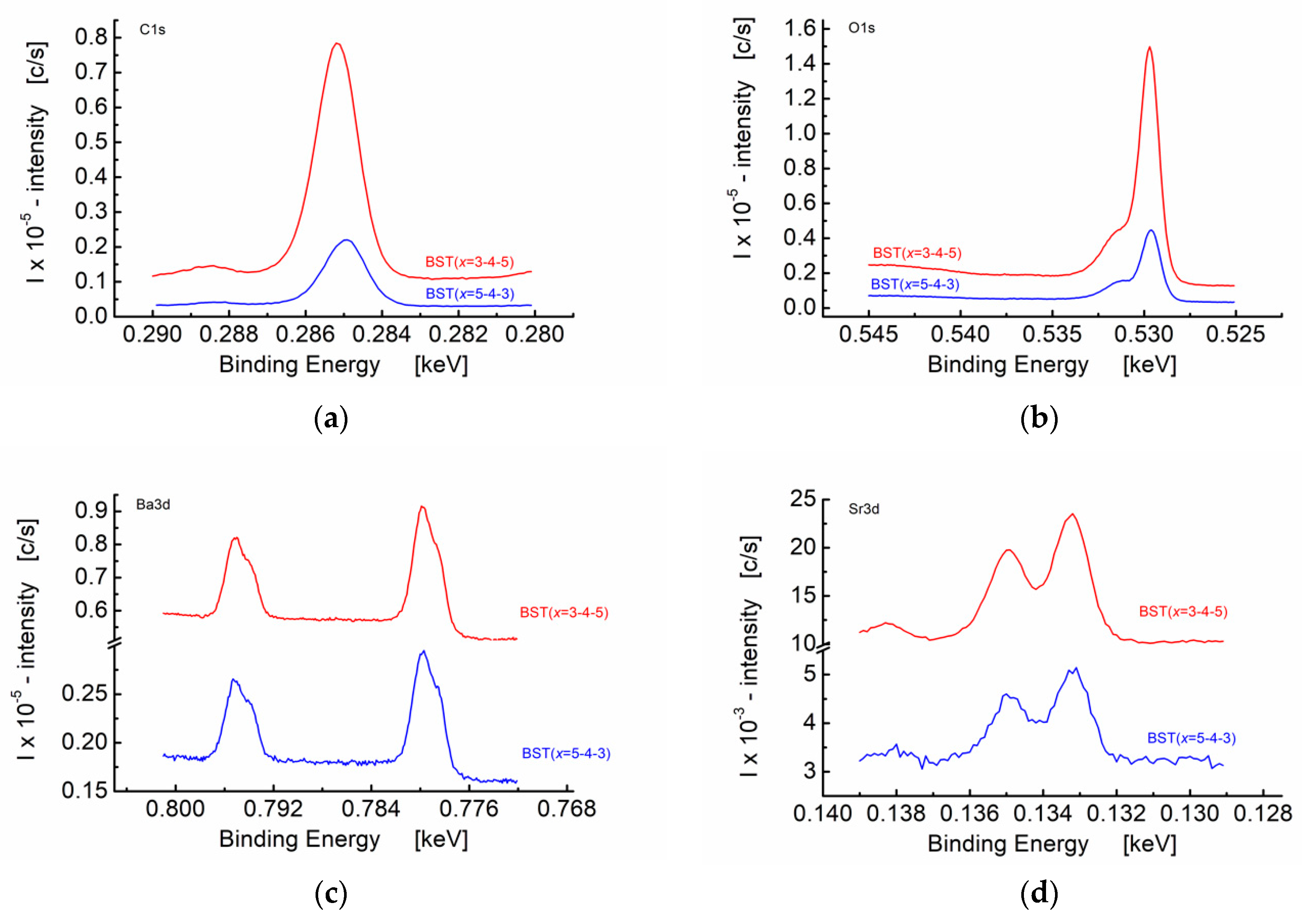
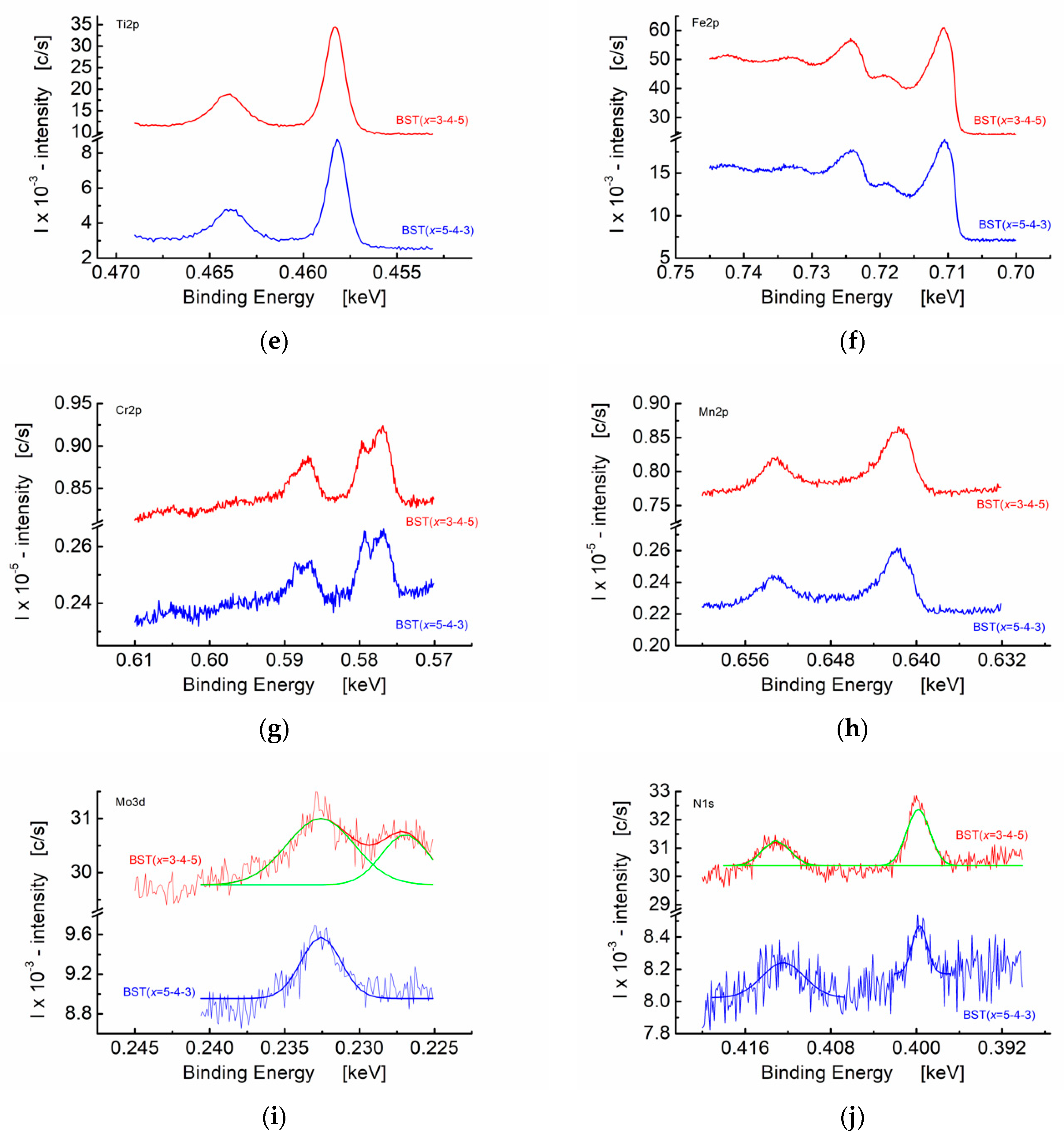
3.3. X-ray Photoelectron Studies of Graded BST Thin Films
4. Conclusions
Author Contributions
Funding
Institutional Review Board Statement
Informed Consent Statement
Data Availability Statement
Acknowledgments
Conflicts of Interest
References
- Jaffe, B.; Cook, W.R.; Jaffe, H. Piezoelectric Ceramics; Academic Press: London, UK, 1971. [Google Scholar]
- Tilley, R.J.D. Perovskites—Structure-Property Relationships; Wiley: Hoboken, NJ, USA, 2016. [Google Scholar]
- Moulson, A.J.; Herbert, J.M. Electroceramics: Materials, Properties, Applications; John Wiley & Sons: Hoboken, NJ, USA, 2003. [Google Scholar]
- Jeon, J.H. Effect of SrTiO3 concentration and sintering temperature on microstructure and dielectric constant of Ba1−xSrxTiO3. J. Eur. Ceram. Soc. 2004, 24, 1045–1048. [Google Scholar] [CrossRef]
- Fu, C.; Cai, W.; Chen, H.; Feng, S.; Pan, F.; Yang, C. Voltage tunable Ba0.6Sr0.4TiO3 thin films and coplanar phase shifters. Thin Solid Films 2008, 516, 5258–5261. [Google Scholar] [CrossRef]
- Zhang, T.; Wang, J.; Zhang, B.; Jiang, J.; Pan, R.; Wang, J. Bottom electrodes dependence of compositionally graded (Ba1−xSrx)TiO3 films. Mater. Res. Bull. 2008, 43, 700–706. [Google Scholar] [CrossRef]
- Zhu, X.-H.; Chan, H.L.-W.; Choy, C.-L.; Wong, K.-H. Influence of ambient oxygen pressure on the preferred orientation, microstructures and dielectric properties of (Ba1−xSrx)TiO3 thin films with compositionally graded structures. Appl. Phys. A 2005, 80, 591–595. [Google Scholar] [CrossRef]
- Gevorgian, S.; Petrov, P.K.; Ivanov, Z.; Wikgorg, E. Tailoring the temperature coefficient of capacitance in ferroelectric varactors. Appl. Phys. Lett. 2001, 79, 1861–1863. [Google Scholar] [CrossRef]
- Wang, J.; Zhang, T.; Xiang, J.; Zhang, B. High-tunability and low-leakage current of the polycrystalline compositionally graded (Ba,Sr)TiO3 thin films derived by a sol–gel process. Mater. Chem. Phys. 2008, 108, 445–448. [Google Scholar] [CrossRef]
- Sbrockey, N.M.; Cole, M.W.; Kalkur, T.S.; Luong, M.; Spanier, J.E.; Tompa, G.S. MOCVD Growth of Compositionally Graded BaxSr1−xTiO3 Thin Films. Integr. Ferroelectr. 2011, 126, 21–27. [Google Scholar] [CrossRef]
- Dewi, R. Optical Characterization of Ba1−xSrxTiO3 Thin Film Properties using Ultraviolet-Visible Spectroscopy. In AIP Conference Proceedings; AIP Publishing LLC.: Melville, NY, USA, 2020; Volume 2219, p. 040001. [Google Scholar] [CrossRef]
- Filho, J.M.C.S.; Ermakov, V.A.; Marques, F.C. Perovskite Thin Film Synthesised from Sputtered Lead Sulphide. Sci. Rep. 2018, 8, 1563. [Google Scholar] [CrossRef] [PubMed]
- Tumarkin, A.; Razumov, S.; Odinets, A.; Gagarin, A.; Altynnikov, A.; Kozyrev, A. Ferroelectric BaSrTiO3 films structured by an intermediate annealing during the deposition. Integr. Ferroelectr. 2016, 173, 38–45. [Google Scholar] [CrossRef]
- Tumarkin, A.; Gagarin, A.; Odinets, A.; Zlygostov, M.; Sapego, E.; Kotelnikov, I. Structural and microwave characterization of BaSrTiO3 thin films deposited on semi-insulating silicon carbide. Jpn. J. Appl. Phys. 2018, 57, 11UE02. [Google Scholar] [CrossRef]
- Gao, L.; Guan, Z.; Huang, S.; Liang, K.; Chen, H.; Zhang, J. Enhanced dielectric properties of barium strontium titanate thin films by doping modification. J. Mater. Sci. Mater. Electron. 2019, 30, 12821–12839. [Google Scholar] [CrossRef]
- Dai, Y.; Schubert, J.; Hollmann, E.; Mussler, G.; Wordenweber, R. Engineering of the Curie temperature of epitaxial Sr1−xBaxTiO3 films via strain. J. Appl. Phys. 2016, 120, 114101. [Google Scholar] [CrossRef]
- Suzuki, T.; Kanno, I.; Loverich, J.J.; Kotera, H.; Wasa, K. Characterization of Pb(Zr,Ti)O3 thin films deposited on stainless steel substrates by RF-magnetron sputtering for MEMS applications. Sens. Actuators A Phys. 2006, 125, 382–386. [Google Scholar] [CrossRef]
- Cardoletti, J.; Komissinskiy, P.; Bruder, E.; Morandi, C.; Alff, L. {001}-textured Pb(Zr,Ti)O3 thin films on stainless steel by pulsed laser deposition. J. Appl. Phys. 2020, 128, 104103. [Google Scholar] [CrossRef]
- Dong, H.; Lu, G.; Chen, D.; Jin, D.; Chen, J.; Cheng, J.J. Effects of LaNiO3 buffer layer on improving the dielectric properties of barium strontium titanate thin films on stainless steel substrates. Sol-Gel Sci. Technol. 2016, 80, 848–852. [Google Scholar] [CrossRef]
- Huang, S.; Chen, J.; Cheng, J. Fabrication and characterization of compositionally graded PbxSr1−xTiO3 thin films by the Sol–gel method. J. Sol-Gel Sci. Technol. 2015, 73, 278–282. [Google Scholar] [CrossRef]
- Bose, A.; Sreemany, M.; Bysakh, S. Influence of processing parameters on the growth characteristics and ferroelectric properties of sputtered PZT thin films on stainless steel substrates. Appl. Surf. Sci. 2013, 282, 202–210. [Google Scholar] [CrossRef]
- Patel, T.A.; Co, K.; Hebert, R.J.; Alpay, S.P. Ferroelectric films on metal substrates, The role of thermal expansion mismatch on dielectric, piezoelectric, and pyroelectric properties. J. Appl. Phys. 2019, 126, 134103. [Google Scholar] [CrossRef]
- Czekaj, D. Fabrication and Study of BST—Based Functional Materials; University of Silesia, Gnome Publishing House: Katowice, Poland, 2010. [Google Scholar]
- Czekaj, D. Technology, Properties and Applications of PZT Thin Films; Wydawnictwo Uniwersytetu Śląskiego: Katowice, Poland, 2002. [Google Scholar]
- Waser, R. (Ed.) Nanoelectronics and Information Technology; Wiley-VCH: Weinheim, Germany, 2005. [Google Scholar]
- Müller, E.; Drašar, Č.; Schilz, J.; Kaysser, W. Functionally graded materials for sensor and energy applications. Mater. Sci. Eng. A 2003, 362, 17–39. [Google Scholar] [CrossRef]
- El-Galy, I.M.; Saleh, B.I.; Ahmed, M.H. Functionally graded materials classifications and development trends from industrial point of view. SN Appl. Sci. 2019, 1, 1378. [Google Scholar] [CrossRef] [Green Version]
- Li, Y.; Feng, Z.; Hao, L.; Huang, L.; Xin, C.; Wang, Y.; Bilotti, E.; Essa, K.; Zhang, H.; Li, Z.; et al. A Review on Functionally Graded Materials and Structures via Additive Manufacturing: From Multi-Scale Design to Versatile Functional Properties. Adv. Mater. Technol. 2020, 5, 1900981. [Google Scholar] [CrossRef]
- Zhang, N.; Khan, T.; Guo, H.; Shi, S.; Zhong, W.; Zhang, W. Functionally Graded Materials: An Overview of Stability, Buckling, and Free Vibration Analysis. Adv. Mater. Sci. Eng. 2019, 2019, 1354150. [Google Scholar] [CrossRef] [Green Version]
- Newnham, R.E.; Skinner, D.P.; Cross, L.E. Connectivity and piezoelectric-pyroelectric composites. Mater. Res. Bull. 1978, 13, 525–536. [Google Scholar] [CrossRef]
- Martin, L.W.; Chu, Y.-H.; Ramesh, R. Advances in the growth and characterization of magnetic, ferroelectric, and multiferroic oxide thin films. Mater. Sci. Eng. 2010, R68, 89–133. [Google Scholar] [CrossRef] [Green Version]
- Schlom, D.G.; Chen, L.-Q.; Eom, C.-B.; Rabe, K.M.; Streiffer, S.K.; Triscone, J.-M. Strain tuning of ferroelectric thin films. Annu. Rev. Mater. Res. 2007, 37, 589. [Google Scholar] [CrossRef] [Green Version]
- Miot, C.; Husson, E.; Proust, C.; Erre, R.; Coutures, J.P. Residual Carbon Evolution in BaTiO3 Ceramics Studied by XPS after Ion Etching. J. Eur. Ceram. Soc. 1988, 18, 339–343. [Google Scholar] [CrossRef]
- ICSD Database. FIZ Karlsruhe. Available online: http://www.fiz-karlsruhe.de (accessed on 10 January 2022).
- International Centre for Diffraction Data. 12 Campus Boulevard, Newton Square, PA 19073-3273 U.S.A. Available online: http://www.icdd.com (accessed on 10 January 2022).
- COD Database. Available online: https://www.crystalimpact.com/match/Default.htm (accessed on 10 January 2022).
- Rietveld, H.M. The Rietveld Method—A Historical Perspective. Austr. J. Phys. 1988, 4, 113–116. [Google Scholar] [CrossRef] [Green Version]
- Ntegra. Available online: http://www.ntmdt-si.com/products (accessed on 10 January 2022).
- NOVA 1.0.26 2004 NT-MDT. Available online: http://www.ntmdt-si.com (accessed on 10 January 2022).
- Czekaj, D.; Lisińska-Czekaj, A. Piezoresponse force microscopy and dielectric spectroscopy study of Ba0.6Sr0.4TiO3 thin films. J. Adv. Dielectr. 2019, 9, 1950025. [Google Scholar] [CrossRef] [Green Version]
- Czekaj, D.; Lisińska-Czekaj, A.; Krzysztofowicz, K. Influence of ceramic coating on mechanical properties of stainless steel. Arch. Metall. Mater. 2020, 65, 911–916. [Google Scholar] [CrossRef]
- Image Analysis P9, NT-MDT. Available online: http://www.ntmdt-si.com/resources (accessed on 10 January 2022).
- Tishkevich, D.; Grabchikov, S.; Zubar, T.; Vasin, D.; Trukhanov, S.; Vorobjova, A.; Yakimchuk, D.; Kozlovskiy, A.; Zdorovets, M.; Giniyatova, S.; et al. Early-Stage Growth Mechanism and Synthesis Conditions-Dependent Morphology of Nanocrystalline Bi Films Electrodeposited from Perchlorate Electrolyte. Nanomaterials 2020, 10, 1245. [Google Scholar] [CrossRef]
- Wagner, C.D.; Riggs, W.M.; Davis, L.E.; Moulder, J.F.; Muilenberg, G.E. (Eds.) Handbook of X-ray Photoelectron Spectroscopy: A Reference Book of Standard Spectra for Identification and Interpretation of XPS Data; Perkin-Elmer: Waltham, MA, USA, 1979. [Google Scholar]
- Wagner, J.M. (Ed.) X-ray Photoelectron Spectroscopy; Nova Science Publishers, Inc.: New York, NY, USA, 2011. [Google Scholar]
- Zdorovets, M.; Kozlovskiy, A.; Tishkevich, D.; Zubar, T.; Trukhanov, A. The effect of doping of TiO2 thin films with low-energy O2+ ions on increasing the efficiency of hydrogen evolution in photocatalytic reactions of water splitting. J. Mater. Sci. Mater. Electron. 2020, 31, 21142–21153. [Google Scholar] [CrossRef]


| Global Parameters | Value | Relevant Parameters of Unit Cell | Value |
|---|---|---|---|
| Profile function | Pseudo-Voigt | Space group (No.) | Imma (74) |
| Background | Polynomial | Lattice parameters: | |
| R (expected), [%]: | 11.05 | a, [Å] | 5.648 |
| R (profile), [%] | 10.01 | b, [Å] | 5.594 |
| R (weighted profile), [%] | 20.84 | c, [Å] | 5.620 |
| GOF | 1.885 | Angle α = β = γ, [°] | 90 |
| d-statistic | 0.10367 | V× 10−6, [pm3] | 177.5975 |
| Global Parameters | Value | Relevant Parameters of Unit Cell | Value |
|---|---|---|---|
| Profile function | Pseudo-Voigt | Space group (No.) | P23 (195) |
| Background | Polynomial | Lattice parameters: | |
| R (expected), [%]: | 11.86 | a, [Å] | 3.966 |
| R (profile), [%] | 8.49 | b, [Å] | 3.966 |
| R (weighted profile), [%] | 20.29 | c, [Å] | 3.966 |
| GOF | 1.711 | Angle α = β = γ [°] | 90 |
| d-statistic | 0.01508 | V× 10−6, [pm3] | 62.37806 |
| Global Parameters | Value (x = 5-4-3) BST | Value (x = 3-4-5) BST |
|---|---|---|
| Profile function | Pseudo-Voigt | Pseudo-Voigt |
| Background | Polynomial | Polynomial |
| R (expected), [%]: | 11.07193 | 11.88390 |
| R (profile), [%] | 13.69155 | 13.47152 |
| R (weighted profile), [%] | 24.94008 | 23.60903 |
| GOF | 5.07398 | 3.94674 |
| d-statistic | 0.06714 | 0.01228 |
| Relevant Parameters | Barium Strontium Titanate (0.67/0.33/1) | Barium Strontium Titanium Oxide (0.59/0.41/1/3) | Barium Strontium Titanate (0.45/0.55/1) | |||
|---|---|---|---|---|---|---|
| Formula sum | O3.00Ti1.00Sr0.33Ba0.67 | O3.00Ti1.00Sr0.41Ba0.59 | O3.00Ti1.00Sr0.55Ba0.45 | |||
| Formula mass, [g/mol] | 216.8239 | 212.9465 | 205.2415 | |||
| Density (calc.), [g/cm3] | 5.7490 | 5.7679 | 5.5852 | 5.5961 | 5.5124 | 5.5191 |
| Weight fraction, [%] | 49.4 | 43.3 | 26.4 | 25.4 | 24.1 | 31.3 |
| Space group (No.) | P 4 m m (99) | P m-3 m (221) | P m-3 m (221) | |||
| Lattice parameters: | ||||||
| a, [Å] | 3.9754(2) | 3.9707(2) | 3.9854(4) | 3.9828(4) | 3.9540(4) | 3.9524(2) |
| b, [Å] | 3.9754(2) | 3.9707(2) | 3.9854(4) | 3.9828(4) | 3.9540(4) | 3.9524(2) |
| c, [Å] | 3.9623(4) | 3.9587(5) | 3.9854(4) | 3.9828(4) | 3.9540(4) | 3.9524(2) |
| Angle α = β = γ, [°] | 90 | 90 | 90 | |||
| V× 10−6, [pm3] | 62.61871 | 62.41287 | 63.30238 | 63.17865 | 61.81735 | 61.74294 |
| x = 5-4-3 BST Film | Area | Average Size | Length | Mean Width | Aspect Ratio | Volume | Perimeter | Diameter |
|---|---|---|---|---|---|---|---|---|
| Unit | μm2 | μm | μm | μm | [1] | μm3 | μm | μm |
| Average | 0.0834 | 0.274 | 0.425 | 0.178 | 2.411 | 4.952 | 1.037 | 0.309 |
| SD | 0.0534 | 0.0907 | 0.154 | 0.0597 | 0.592 | 4.876 | 0.488 | 0.102 |
| x = 3-4-5 BST Film | Area | Average Size | Length | Mean Width | Aspect Ratio | Volume | Perimeter | Diameter |
|---|---|---|---|---|---|---|---|---|
| Unit | μm2 | μm | μm | μm | [1] | μm3 | μm | μm |
| Average | 0.0455 | 0.201 | 0.316 | 0.130 | 2.463 | 1.590 | 0.787 | 0.227 |
| SD | 0.0304 | 0.0698 | 0.120 | 0.0454 | 0.647 | 1.775 | 0.376 | 0.0787 |
| Element/Value | Ti 2p | Sr 3p3 | Ba 3d3 |
|---|---|---|---|
| BST (x = 3-4-5), [at.%] | 48.06 | 31.38 | 20.56 |
| BST (x = 5-4-3), [at.%] | 16.43 | 72.31 | 11.26 |
| Element/Value | Ti 2p | Sr 3d | Ba 3d3 |
|---|---|---|---|
| BST (x = 3-4-5), [at.%] | 47.80 | 30.73 | 21.47 |
| BST (x = 5-4-3), [at.%] | 48.06 | 18.68 | 33.26 |
Publisher’s Note: MDPI stays neutral with regard to jurisdictional claims in published maps and institutional affiliations. |
© 2022 by the authors. Licensee MDPI, Basel, Switzerland. This article is an open access article distributed under the terms and conditions of the Creative Commons Attribution (CC BY) license (https://creativecommons.org/licenses/by/4.0/).
Share and Cite
Lisińska-Czekaj, A.; Czekaj, D. Study of the Layer-Type BST Thin Film with X-ray Diffraction and X-ray Photoelectron Spectroscopy. Materials 2022, 15, 578. https://doi.org/10.3390/ma15020578
Lisińska-Czekaj A, Czekaj D. Study of the Layer-Type BST Thin Film with X-ray Diffraction and X-ray Photoelectron Spectroscopy. Materials. 2022; 15(2):578. https://doi.org/10.3390/ma15020578
Chicago/Turabian StyleLisińska-Czekaj, Agata, and Dionizy Czekaj. 2022. "Study of the Layer-Type BST Thin Film with X-ray Diffraction and X-ray Photoelectron Spectroscopy" Materials 15, no. 2: 578. https://doi.org/10.3390/ma15020578
APA StyleLisińska-Czekaj, A., & Czekaj, D. (2022). Study of the Layer-Type BST Thin Film with X-ray Diffraction and X-ray Photoelectron Spectroscopy. Materials, 15(2), 578. https://doi.org/10.3390/ma15020578