Abstract
In this work, a hydrogen-terminated (H-terminated) diamond field effect transistor (FET) with HfAlOx/Al2O3 bilayer dielectrics is fabricated and characterized. The HfAlOx/Al2O3 bilayer dielectrics are deposited by the atomic layer deposition (ALD) technique, which can protect the H-terminated diamond two-dimensional hole gas (2DHG) channel. The device demonstrates normally-on characteristics, whose threshold voltage (VTH) is 8.3 V. The maximum drain source current density (IDSmax), transconductance (Gm), capacitance (COX) and carrier density (ρ) are −6.3 mA/mm, 0.73 mS/mm, 0.22 μF/cm2 and 1.53 × 1013 cm−2, respectively.
1. Introduction
The diamond is considered as an ultimate semiconductor with ultrawide bandgap of 5.47 eV, extremely high breakdown field of 10 MV/cm, highest thermal conductivity of 22 W/cm·K, high carrier mobility (electrons of 4500 cm2/V·s, holes of 3800 cm2/V·s) and large carrier saturation velocity (electrons of 1.5–2.7 × 107 cm/s, holes of 0.85–1.2 × 107 cm/s) [1,2,3,4]. Since the dopants cannot be activated at room temperature with high activation energy (boron of 370 meV and phosphorous of 650 meV) [5], the application of diamonds has been greatly hindered. In this case, δ-doping comes into being. However, this technique requires the precise control of the doping thickness, and the carrier mobility is not ideal [5]. Fortunately, a hydrogen-terminated (H-terminated) diamond with two-dimensional hole gas (2DHG) channel provides a new solution to overcome these problems, which demonstrates a high carrier density of 1013 cm−2 and large carrier mobility of 50–200 cm2/V·s [3,6]. To date, as a promising structure of diamond-based electronic devices, the H-terminated diamond field effect transistor (FET) has aroused the great interest of researchers [7,8,9,10,11,12,13,14,15,16,17,18,19,20,21].
Since a H-terminated diamond is thermally and chemically instable, it is necessary to stabilize the hole carriers for a H-terminated diamond FET with a dielectric layer [8]. Furthermore, the dielectric material with high dielectric constant can control large charge responses at a small bias effectively [14]. To date, many high dielectric constant materials have been employed for the fabrication of a H-terminated diamond FET [10,15]. However, there are few reports on using HfAlOX as dielectric with a high dielectric constant, high crystallization temperature and large band gap (5.8–6.2 eV). [22].
In this work, we study a H-terminated diamond FET with HfAlOx/Al2O3 bilayer dielectrics, and its electrical properties were evaluated by semiconductor analyzer.
2. Materials and Methods
The fabrication process of the H-terminated diamond FET with HfAlOx/Al2O3 bilayer dielectrics is displayed in Figure 1. A high temperature and high pressure (HPHT) single crystal diamond substrate was cleaned by various solutions before growth [9]. Then, a 200 nm homoepitaxy layer was grown on the substrate with the dimensions of 3 × 3 × 0.5 mm3 by the microwave plasma chemical vapor deposition (MPCVD) technique. The growth conditions were declared in our previous work [9]. Afterwards, 150 nm Au electrodes with 20 μm source drain gap (LSD) were realized by photolithography, electron beam evaporation (EB) and the lift-off technique. Next, isolation was carried out with 20 min UV/ozone treatment. After that, a 4 nm Al2O3 film was deposited to protect the H-terminated channel, and a 30 nm HfAlOx film was deposited by the ALD technique sequentially. The atomic percentage of HfAlOx is Hf:Al:O = 2:23:75, evaluated by the energy dispersive X-ray spectroscopy (EDS) technique. Finally, 150 nm Al gate electrode was deposited on the gate region with 4 μm gate length (LG) and 100 μm gate width (WG). The electrical properties of this device were characterized by Agilent B1505A. Figure 2 demonstrates the schematic diagram of the H-terminated diamond FET with HfAlOx/Al2O3 bilayer dielectrics. The electrical contacts for the source, drain and gate electrodes are exhibited, and the hole carriers of the channel are illustrated.
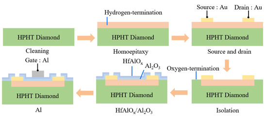
Figure 1.
Fabrication process of the H-terminated diamond FET with HfAlOx/Al2O3 bilayer dielectrics.
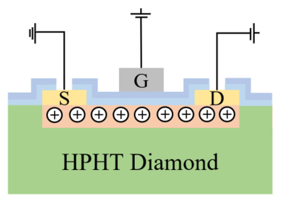
Figure 2.
Schematic diagram of the H-terminated diamond FET with HfAlOx/Al2O3 bilayer dielectrics.
3. Results and Discussion
Figure 3a demonstrates the drain source current density (IDS) versus drain source voltage (VDS) at different gate voltages (VGS) of the H-terminated diamond FET with HfAlOx/Al2O3 bilayer dielectrics. The gate length (LG), gate width (WG) and LSD for the device are 4 μm, 100 μm and 20 μm, respectively. The VGS varies from 8 to −6 V in a step of −2 V. The absolute value of IDS (|IDS|) increases as the absolute value of the VGS (|VGS|) increases, indicating the existence of a p-type channel. The maximum IDS (IDSmax) is −6.3 mA/mm obtained at a VGS of −6 V and a VDS of −20 V. The IDSmax is relatively large compared with our previous work [13,23], and the reason may be attributed to the undamaged 2DHG conduction channel protected by Al2O3.
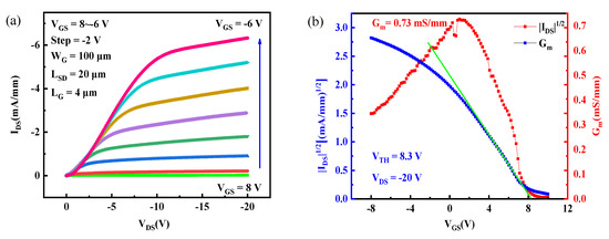
Figure 3.
Characteristics of the H-terminated diamond FET with HfAlOx/Al2O3 bilayer dielectrics: (a) output and (b) transfer.
In Figure 3b, the transfer characteristic of the H-terminated diamond FET with HfAlOx/Al2O3 bilayer dielectrics is presented. The threshold voltage (VTH) is extrapolated to be 8.3 V at a VDS of −20 V based on the relationship between |IDS|1/2 and VGS, demonstrating normally-on characteristics [14]. The maximum transconductance (Gm) is 0.73 mS/mm.
The leakage current density (IGS) in the log coordinate of the H-terminated diamond FET with HfAlOx/Al2O3 bilayer dielectrics is shown in Figure 4a. The VGS changes from −6 to 8 V, and the absolute value of IGS (|IGS|) is 7.95 × 10⁻⁷ A/cm2 at a VGS of −6 V, demonstrating a low |IGS|. Table 1 demonstrates the |IGS| comparison with the reported H-terminated FETs. The |IGS| for the MoO3, LiF/Al2O3, Ta2O5/Al2O3 and ZrO2/Al2O3 H-terminated diamond FET are 3.33 × 10⁻⁴ A/cm2, 1 × 10⁻⁶ A/cm2, 7.6 × 10⁻⁴ A/cm2 and 4.8 × 10⁻⁵ A/cm2, respectively [21,24,25,26]. Their values are larger than those of the HfAlOx/Al2O3 FET. As shown in Figure 4b, the relationship between IGS and VGS can be described by the thermionic field emission (TFE) model (1) [9]:
where JTFE means the IGS caused by TFE model; JS represents the saturation current; and P is a parameter associated with the carrier tunneling probability and temperature [9]. In Figure 4b, the lnJTFE/JS(−exp(qV/kT)) and VGS exhibit a linear relationship under the TFE model.
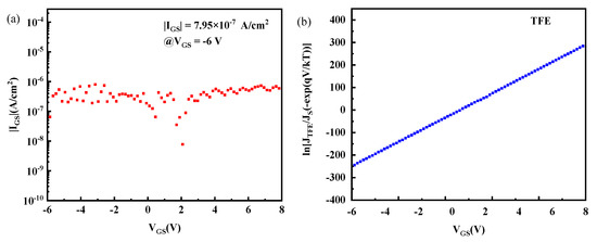
Figure 4.
IGS characteristics of the H-terminated diamond FET with HfAlOx/Al2O3 bilayer dielectrics: (a) |IGS| and (b) TFE.

Table 1.
The |IGS| comparison between this work and the reported H-terminated diamond FETs.
Figure 5a displays the capacitance-voltage (C-V) curve measured at 1 MHz of the H-terminated diamond FET with HfAlOx/Al2O3 bilayer dielectrics. Evident accumulation and depletion regions can be observed. The maximum capacitance (COX) is 0.22 μF/cm2 at VGS of −2 V. Based on the method d2C/d2VGS = 0, the flat band voltage (VFB) is determined to be 8.5 V and 7.6 V in the forward and reverse directions, respectively [18]. The trapped charge density is evaluated to be 1.24 × 1012 cm−2 based on the hysteresis voltage of 0.9 V [8]. Additionally, the CV curve shifts to the positive direction, indicating the presence of fixed negative charge in the dielectric layer. This increases the hole carriers in the 2DHG channel, thus resulting in a normally-on operation. The fixed negative charge density is deduced to be 1.25 × 1013 cm−2 on the basis of COX, VFB, and the work function difference between Al and the H-terminated diamond [8]. In addition, the dielectric constant of HfAlOx/Al2O3 is calculated to be 8.45, suggesting that the quality of HfAlOx/Al2O3 needs to be further improved. As demonstrated in Figure 5b, the carrier density (ρ) is 1.50 × 1013 cm−2 at the VGS of −2 V evaluated based on [18]. The ρ is large, and this can be attributed to the high quality of the H-terminated diamond [8,21].
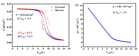
Figure 5.
Characteristics of the H-terminated diamond FET with HfAlOx/Al2O3 bilayer dielectrics measured at 1 MHz: (a) C-V and (b) ρ.
4. Conclusions
In summary, the electrical properties of H-terminated diamond FET with HfAlOx/Al2O3 bilayer dielectrics were investigated. The output characteristics demonstrate an evident p-type channel, and the IDSmax is −6.3 mA/mm obtained at VGS of −6 V. The transfer characteristics exhibits the VTH of 8.3 V, indicating normally-on characteristics. The |IGS| is 7.95 × 10⁻⁷ A/cm2 at a VGS of −6 V, demonstrating a low |IGS|. In addition, the COX is 0.22 μF/cm2 based on the C-V curve. Additionally, the ρ is 1.50 × 1013 cm−2 at a VGS of −2 V. The results are meaningful for the research of a H-terminated diamond FET, and the electrical performance of HfAlOx/Al2O3 FET will be further improved by optimizing the fabrication process in our future work.
Author Contributions
Conceptualization, M.Z., W.W. and S.F.; methodology, M.Z. and F.L.; software, M.Z. and G.C.; validation, W.W. and H.W.; formal analysis, F.W.; investigation, M.Z. and S.H.; resources, M.Z. and Y.W.; data curation, M.Z. and F.L.; writing—original draft preparation, M.Z.; writing—review and editing, M.Z., W.W. and H.W.; visualization, R.B.; supervision, W.W. and H.W.; project administration, M.Z.; funding acquisition, W.W. and H.W. All authors have read and agreed to the published version of the manuscript.
Funding
This work was funded by National Key R&D Program of China (No. 2018YFE0125900), National Natural Science Foundation of China (No. 61627812, 61804122 and 62074127), China Postdoctoral Science Foundation (No. 2019M660256 and 2020M683485), and Key R&D Program of Shaanxi Province (No. 2021GY-223).
Institutional Review Board Statement
Not applicable.
Informed Consent Statement
Not applicable.
Data Availability Statement
Data are contained within the article.
Conflicts of Interest
The authors declare no conflict of interest.
References
- Isberg, J.; Hammersberg, J.; Johansson, E.; Wikström, T.; Twitchen, D.J.; Whitehead, A.J.; Coe, S.E.; Scarsbrook, G.A. High carrier mobility in single-crystal plasma-deposited diamond. Science 2002, 297, 1670–1672. [Google Scholar] [CrossRef] [PubMed]
- Maier, F.; Riedel, M.; Mantel, B.; Ristein, J.; Ley, L. Origin of surface conductivity in diamond. Phys. Rev. Lett. 2000, 85, 3472–3475. [Google Scholar] [CrossRef] [PubMed]
- Crawford, K.G.; Weil, J.D.; Shah, P.B.; Ruzmetov, D.A.; Neupane, M.R.; Kingkeo, K.; Birdwell, A.G.; Ivanv, T.G. Diamond field-effect transistors with V2O5-induced transfer doping: Scaling to 50-nm gate length. IEEE Trans. Electron Devices 2020, 67, 2270–2275. [Google Scholar] [CrossRef]
- Liu, J.W.; Teraji, T.; Da, B.; Ohsato, H.; Koide, Y. Effect of annealing temperature on performances of boron-doped diamond metal-semiconductor field-effect transistors. IEEE Trans. Electron Devices 2020, 67, 1680–1685. [Google Scholar] [CrossRef]
- Wang, W.; Fu, K.; Hu, C.; Li, F.N.; Liu, Z.C.; Li, S.Y.; Lin, F.; Fu, J.; Wang, J.J.; Wang, H.X. Diamond based field-effect transistors with SiNx and ZrO2 double dielectric layers. Diam. Relat. Mater. 2016, 69, 237–240. [Google Scholar] [CrossRef]
- Kawarada, H. Hydrogen-terminated diamond surfaces and interfaces. Surf. Sci. Rep. 1996, 26, 205–259. [Google Scholar] [CrossRef]
- Liao, M.Y.; Sang, L.W.; Shimaoka, T.; Imura, M.; Koizumi, S.; Koide, Y. Energy-efficient metal-insulator-metal-semiconductor field-effect transistors based on 2D carrier gases. Adv. Electron. Mater. 2019, 5, 1800832. [Google Scholar] [CrossRef]
- Wang, W.; Wang, Y.F.; Zhang, M.H.; Wang, R.Z.; Chen, G.Q.; Chang, X.H.; Lin, F.; Wen, F.; Jia, K.; Wang, H.X. An enhancement-mode hydrogen-terminated diamond field-effect transistor with lanthanum hexaboride gate material. IEEE Electron Device Lett. 2020, 41, 585–588. [Google Scholar] [CrossRef]
- Zhang, M.H.; Wang, W.; Fan, S.W.; Chen, G.Q.; Abbasi, H.N.; Lin, F.; Wen, F.; Zhang, J.W.; Bu, R.A.; Wang, H.X. Normally-off hydrogen-terminated diamond field effect transistor with yttrium gate. Carbon 2021, 176, 307–312. [Google Scholar] [CrossRef]
- Liu, J.W.; Liao, M.Y.; Imura, M.; Koide, Y. High-k ZrO2/Al2O3 bilayer on hydrogenated diamond: Band configuration, breakdown field, and electrical properties of field-effect transistors. J. Appl. Phys. 2016, 120, 124504. [Google Scholar] [CrossRef]
- Liu, J.W.; Liao, M.Y.; Imura, M.; Matsumoto, T.; Shibata, N.; Ikuhara, Y.; Koide, Y. Control of normally on/off characteristics in hydrogenated diamond metal-insulator-semiconductor field-effect transistors. J. Appl. Phys. 2015, 118, 115704. [Google Scholar] [CrossRef]
- Zhang, M.H.; Wang, W.; Chen, G.Q.; Abbasi, H.N.; Lin, F.; Wen, F.; Wang, K.Y.; Zhang, J.W.; Bu, R.A.; Wang, H.X. Electrical properties of yttrium gate hydrogen-terminated diamond field effect transistor with Al2O3 dielectric layer. Appl. Phys. Lett. 2021, 118, 053506. [Google Scholar] [CrossRef]
- Wang, W.; Hu, C.; Li, S.Y.; Li, F.N.; Liu, Z.C.; Wang, F.; Fu, J.; Wang, H.X. Diamond based field—Effect transistors of Zr gate with SiNx dielectric layers. J. Nanomater. 2015, 2015, 124640. [Google Scholar] [CrossRef] [Green Version]
- Liu, J.W.; Liao, M.Y.; Imura, M.; Koide, Y. Normally-off HfO2-gated diamond field effect transistors. Appl. Phys. Lett. 2013, 103, 092905. [Google Scholar] [CrossRef]
- Dong, H.K.; Shi, L.B. Impact of native defects in the high dielectric constant oxide HfSiO4 on MOS device performance. Chin. Phys. Lett. 2016, 33, 016101. [Google Scholar] [CrossRef]
- Liu, J.W.; Oosato, H.; Liao, M.Y.; Koide, Y. Enhancement-mode hydrogenated diamond metal-oxide-semiconductor field-effect transistors with Y2O3 oxide insulator grown by electron beam evaporator. Appl. Phys. Lett. 2017, 110, 203502. [Google Scholar] [CrossRef]
- Hayashi, K.; Yamanaka, S.; Watanabe, H.; Sekiguchi, T.; Okushi, H.; Kajimura, K. Investigation of the effect of hydrogen on electrical and optical properties in chemical vapor deposited on homoepitaxial diamond films. J. Appl. Phys. 1997, 81, 744–753. [Google Scholar] [CrossRef]
- Zhang, J.F.; Chen, W.J.; Ren, Z.Y.; Su, K.; Yang, P.Z.; Hu, Z.Z.; Zhang, J.C.; Hao, Y. Characterization and mobility analysis of normally off hydrogen-terminated diamond metal–oxide–semiconductor field-effect transistors. Phys. Status Solidi A 2020, 217, 1900462. [Google Scholar] [CrossRef]
- Chicot, G.; Marechal, A.; Motte, R.; Muret, P.; Gheeraert, E.; Pernot, J. Metal oxide semiconductor structure using oxygen-terminated diamond. Appl. Phys. Lett. 2013, 102, 242108. [Google Scholar] [CrossRef] [Green Version]
- Fei, W.X.; Bi, T.; Iwataki, M.; Imanishi, S.; Kawarada, H. Oxidized Si terminated diamond and its MOSFET operation with SiO2 gate insulator. Appl. Phys. Lett. 2020, 116, 269901. [Google Scholar] [CrossRef]
- Ren, Z.Y.; Zhang, J.F.; Zhang, J.C.; Zhang, C.F.; Xu, S.R.; Li, Y.; Hao, Y. Diamond field effect transistors with MoO3 gate dielectric. IEEE Electron Device Lett. 2017, 38, 786–789. [Google Scholar] [CrossRef]
- Mallik, S.; Mahata, C.; Hota, M.K.; Dalapati, G.K.; Chi, D.Z.; Sarkar, C.K.; Maiti, C.K. HfAlOx high-k gate dielectric on SiGe: Interfacial reaction, energy-band alignment, and charge trapping properties. Microelectron. Eng. 2010, 87, 2234–2240. [Google Scholar] [CrossRef]
- Wang, Y.F.; Wang, W.; Chang, X.H.; Abbasi, H.N.; Zhang, X.F.; Wang, R.Z.; Wang, H.X. Performance of hydrogen-terminated diamond MOSFET with bilayer dielectrics of YSZ/Al2O3. Diam. Relat. Mater. 2019, 99, 107532. [Google Scholar] [CrossRef]
- Wang, Y.F.; Wang, W.; Abbasi, H.N.; Chang, X.H.; Zhang, X.F.; Zhu, T.F.; Liu, Z.C.; Song, W.Z.; Chen, G.Q.; Wang, H.X. LiF/Al2O3 as dielectrics for MOSFET on single crystal hydrogen-terminated diamond. IEEE Electron Device Lett. 2020, 41, 808–811. [Google Scholar] [CrossRef]
- Liu, J.W.; Liao, M.Y.; Imura, M.; Watanabe, E.; Oosato, H.; Koide, Y. Diamond field effect transistors with a high-dielectric constant Ta2O5 as gate material. J. Phys. D Appl. Phys. 2014, 47, 245102. [Google Scholar] [CrossRef]
- Liu, J.W.; Liao, M.Y.; Imura, M.; Tanaka, A.; Iwai, H.; Koide, Y. Low on-resistance diamond field effect transistor with high-k ZrO2 as dielectric. Sci. Rep. 2014, 4, 6395. [Google Scholar] [CrossRef] [Green Version]
Publisher’s Note: MDPI stays neutral with regard to jurisdictional claims in published maps and institutional affiliations. |
© 2022 by the authors. Licensee MDPI, Basel, Switzerland. This article is an open access article distributed under the terms and conditions of the Creative Commons Attribution (CC BY) license (https://creativecommons.org/licenses/by/4.0/).