
First-Principles Study of Cu-Based Inorganic Hole Transport Materials for Solar Cell Applications


Abstract
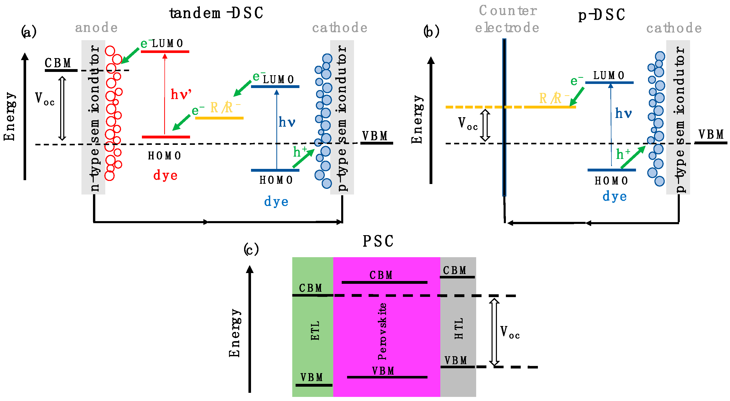
:1. Introduction
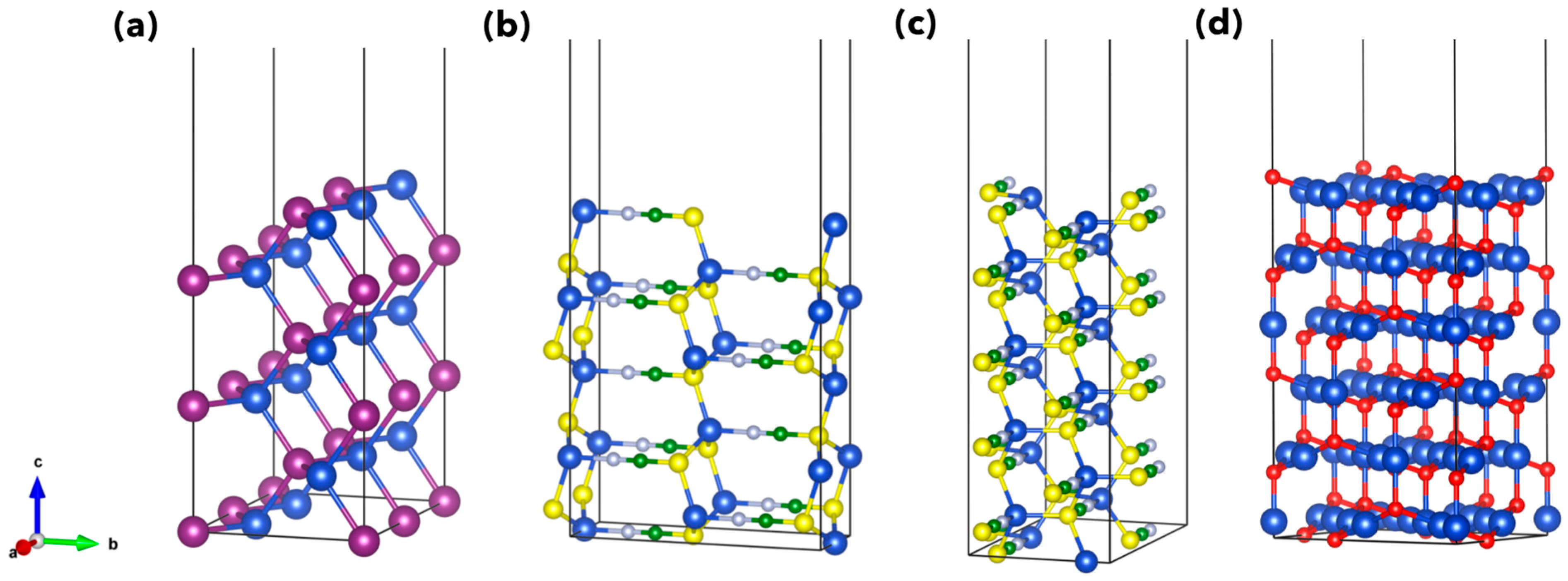
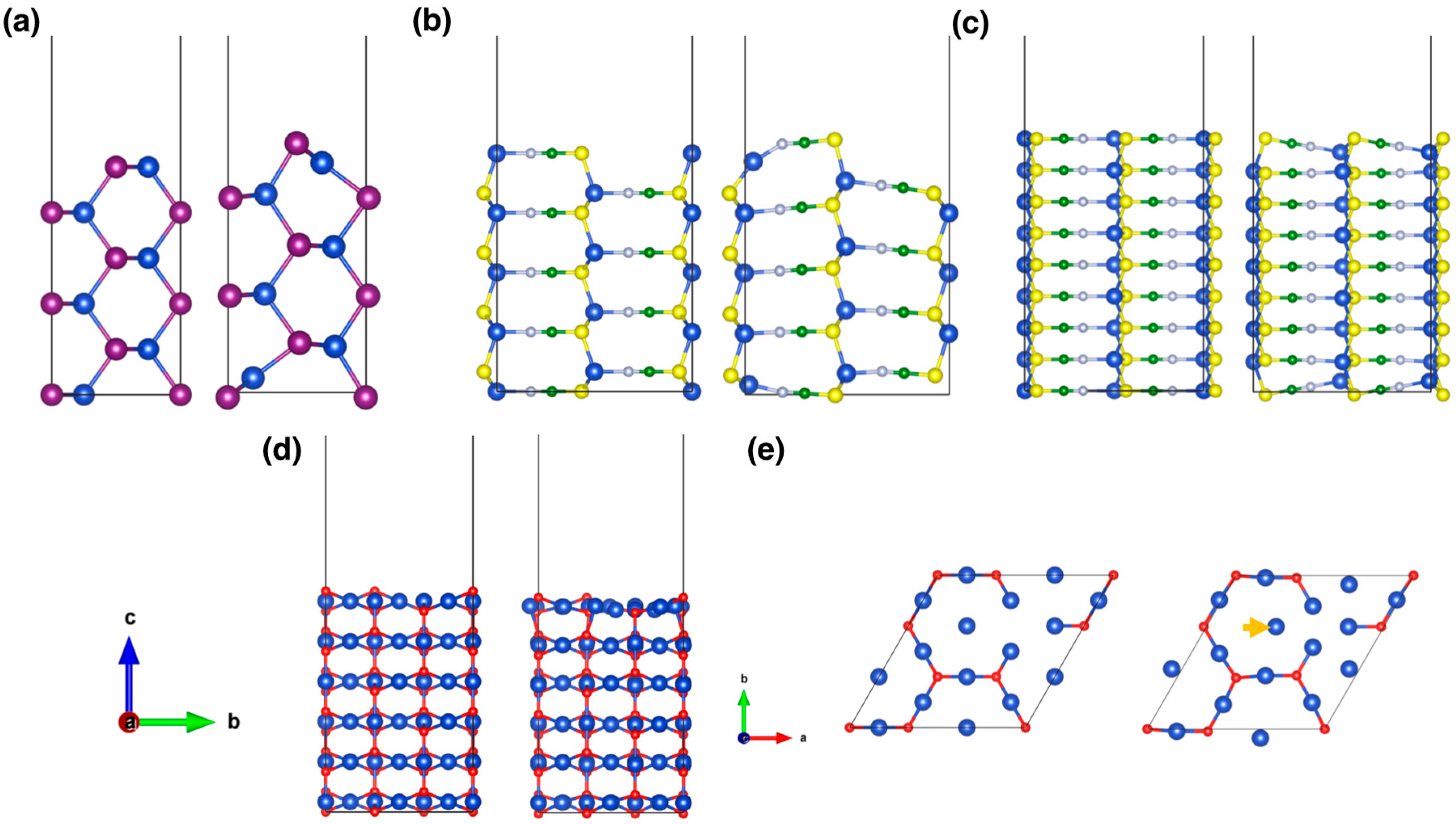
2. Computational Details
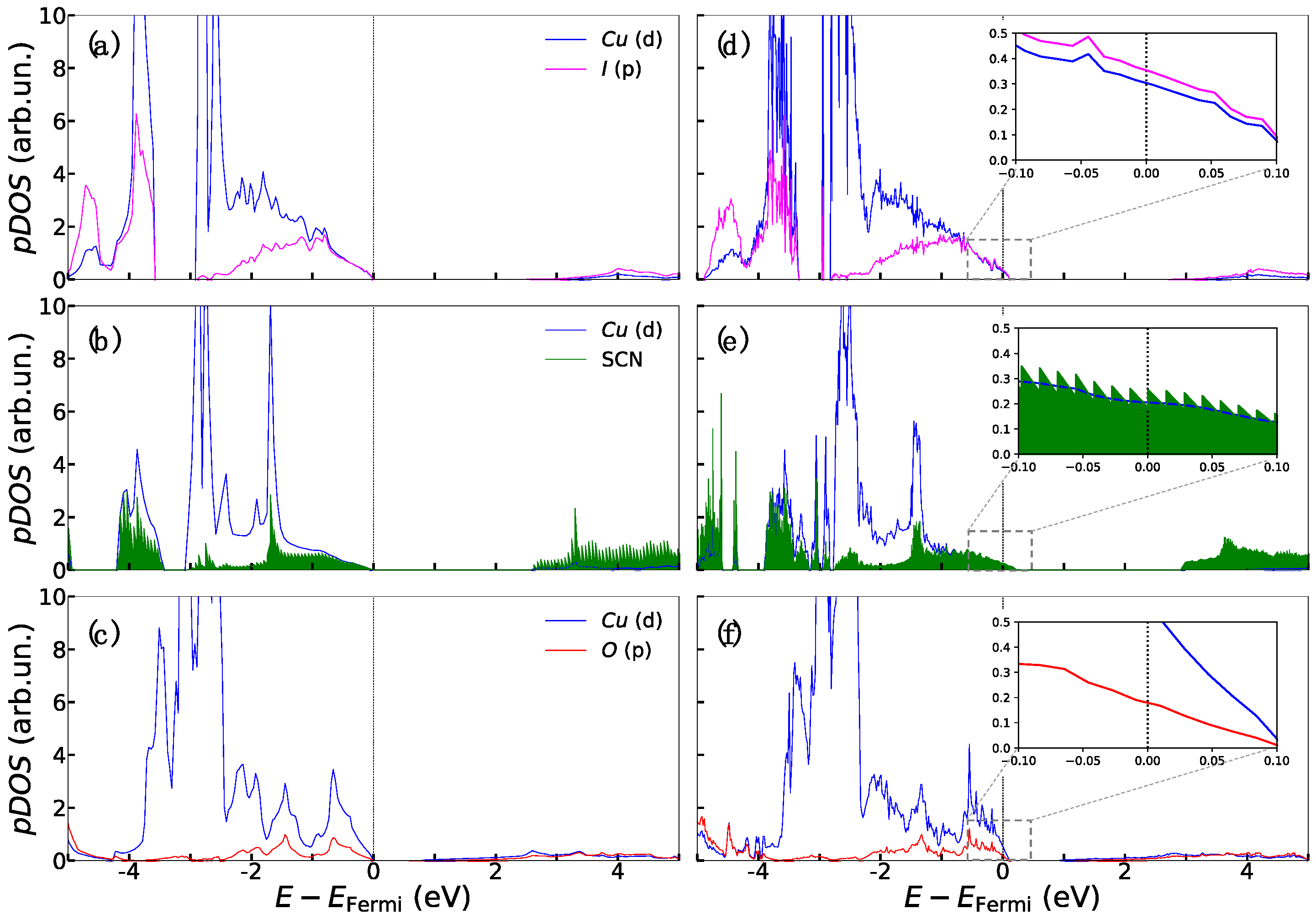
3. Results and Discussion
4. Conclusions
Supplementary Materials
Author Contributions
Funding
Institutional Review Board Statement
Informed Consent Statement
Acknowledgments
Conflicts of Interest
References
- O’Regan, B.; Grätzel, M. A low-cost, high-efficiency solar cell based on dye-sensitized colloidal TiO2 films. Nature 1991, 353, 737–740. [Google Scholar] [CrossRef]
- Kim, J.Y.; Lee, J.-W.; Jung, H.S.; Shin, H.; Park, N.-G. High-Efficiency Perovskite Solar Cells. Chem. Rev. 2020, 120, 7867–7918. [Google Scholar] [CrossRef] [PubMed]
- Muñoz-García, A.B.; Benesperi, I.; Boschloo, G.; Concepcion, J.J.; Delcamp, J.H.; Gibson, E.A.; Meyer, G.J.; Pavone, M.; Pettersson, H.; Hagfeldt, A.; et al. Dye-sensitized solar cells strike back. Chem. Soc. Rev. 2021, 50, 12450–12550. [Google Scholar] [CrossRef] [PubMed]
- Zhang, D.; Stojanovic, M.; Ren, Y.; Cao, Y.; Eickemeyer, F.T.; Socie, E.; Vlachopoulos, N.; Moser, J.-E.; Zakeeruddin, S.M.; Hagfeldt, A.; et al. A molecular photosensitizer achieves a Voc of 1.24 V enabling highly efficient and stable dye-sensitized solar cells with copper(II/I)-based electrolyte. Nat. Commun. 2021, 12, 1777. [Google Scholar] [CrossRef]
- Ji, J.-M.; Zhou, H.; Eom, Y.K.; Kim, C.H.; Kim, H.K. 14.2% Efficiency Dye-Sensitized Solar Cells by Co-sensitizing Novel Thieno[3,2-b]indole-Based Organic Dyes with a Promising Porphyrin Sensitizer. Adv. Energy Mater. 2020, 10, 2000124. [Google Scholar] [CrossRef]
- Xiong, D.; Chen, W. Recent progress on tandem structured dye-sensitized solar cells. Front. Optoelectron. 2012, 5, 371–389. [Google Scholar] [CrossRef]
- Tian, H. Solid-state p-type dye-sensitized solar cells: Progress, potential applications and challenges. Sustain. Energy Fuels 2019, 3, 888–898. [Google Scholar] [CrossRef]
- Jeong, J.; Kim, M.; Seo, J.; Lu, H.; Ahlawat, P.; Mishra, A.; Yang, Y.; Hope, M.A.; Eickemeyer, F.T.; Kim, M.; et al. Pseudo-halide anion engineering for α-FAPbI3 perovskite solar cells. Nature 2021, 592, 381–385. [Google Scholar] [CrossRef]
- Kim, H.-S.; Lee, C.-R.; Im, J.-H.; Lee, K.-B.; Moehl, T.; Marchioro, A.; Moon, S.-J.; Humphry-Baker, R.; Yum, J.-H.; Moser, J.E.; et al. Lead Iodide Perovskite Sensitized All-Solid-State Submicron Thin Film Mesoscopic Solar Cell with Efficiency Exceeding 9%. Sci. Rep. 2012, 2, 591. [Google Scholar] [CrossRef]
- Kojima, A.; Teshima, K.; Shirai, Y.; Miyasaka, T. Organometal Halide Perovskites as Visible-Light Sensitizers for Photovoltaic Cells. J. Am. Chem. Soc. 2009, 131, 6050–6051. [Google Scholar] [CrossRef]
- Jena, A.K.; Kulkarni, A.; Miyasaka, T. Halide Perovskite Photovoltaics: Background, Status, and Future Prospects. Chem. Rev. 2019, 119, 3036–3103. [Google Scholar] [CrossRef] [PubMed]
- Vitoratos, E.; Sakkopoulos, S.; Dalas, E.; Paliatsas, N.; Karageorgopoulos, D.; Petraki, F.; Kennou, S.; Choulis, S.A. Thermal degradation mechanisms of PEDOT:PSS. Org. Electron. 2009, 10, 61–66. [Google Scholar] [CrossRef]
- Girolamo, D.D.; Giacomo, F.D.; Matteocci, F.; Giacomo Marrani, A.; Dini, D.; Abate, A. Progress, highlights and perspectives on NiO in perovskite photovoltaics. Chem. Sci. 2020, 11, 7746–7759. [Google Scholar] [CrossRef]
- Di Girolamo, D.; Matteocci, F.; Kosasih, F.U.; Chistiakova, G.; Zuo, W.; Divitini, G.; Korte, L.; Ducati, C.; Di Carlo, A.; Dini, D.; et al. Stability and Dark Hysteresis Correlate in NiO-Based Perovskite Solar Cells. Adv. Energy Mater. 2019, 9, 1901642. [Google Scholar] [CrossRef]
- Ito, S.; Tanaka, S.; Vahlman, H.; Nishino, H.; Manabe, K.; Lund, P. Carbon-Double-Bond-Free Printed Solar Cells from TiO2/CH3NH3PbI3/CuSCN/Au: Structural Control and Photoaging Effects. ChemPhysChem 2014, 15, 1194–1200. [Google Scholar] [CrossRef] [PubMed]
- Odobel, F.; Pellegrin, Y. Recent Advances in the Sensitization of Wide-Band-Gap Nanostructured p-Type Semiconductors. Photovoltaic and Photocatalytic Applications. J. Phys. Chem. Lett. 2013, 4, 2551–2564. [Google Scholar] [CrossRef]
- Baiano, C.; Schiavo, E.; Gerbaldi, C.; Bella, F.; Meligrana, G.; Talarico, G.; Maddalena, P.; Pavone, M.; Muñoz-García, A.B. Role of surface defects in CO2 adsorption and activation on CuFeO2 delafossite oxide. Mol. Catal. 2020, 496, 111181. [Google Scholar] [CrossRef]
- Gharibzadeh, S.; Nejand, B.A.; Moshaii, A.; Mohammadian, N.; Alizadeh, A.H.; Mohammadpour, R.; Ahmadi, V.; Alizadeh, A. Two-Step Physical Deposition of a Compact CuI Hole-Transport Layer and the Formation of an Interfacial Species in Perovskite Solar Cells. ChemSusChem 2016, 9, 1929–1937. [Google Scholar] [CrossRef]
- Srivastava, R.P.; Jung, H.-S.; Khang, D.-Y. Transfer-Printed Cuprous Iodide (CuI) Hole Transporting Layer for Low Temperature Processed Perovskite Solar Cells. Nanomaterials 2022, 12, 1467. [Google Scholar] [CrossRef]
- Sepalage, G.A.; Meyer, S.; Pascoe, A.R.; Scully, A.D.; Bach, U.; Cheng, Y.-B.; Spiccia, L. A facile deposition method for CuSCN: Exploring the influence of CuSCN on J-V hysteresis in planar perovskite solar cells. Nano Energy 2017, 32, 310–319. [Google Scholar] [CrossRef]
- Bredar, A.R.C.; Blanchet, M.D.; Comes, R.B.; Farnum, B.H. Evidence and Influence of Copper Vacancies in p-Type CuGaO2 Mesoporous Films. ACS Appl. Energy Mater. 2019, 2, 19–28. [Google Scholar] [CrossRef]
- Schiavo, E.; Latouche, C.; Barone, V.; Crescenzi, O.; Muñoz-García, A.B.; Pavone, M. An ab initio study of Cu-based delafossites as an alternative to nickel oxide in photocathodes: Effects of Mg-doping and surface electronic features. Phys. Chem. Chem. Phys. 2018, 20, 14082–14089. [Google Scholar] [CrossRef] [PubMed]
- Muñoz-García, A.B.; Caputo, L.; Schiavo, E.; Baiano, C.; Maddalena, P.; Pavone, M. Ab initio Study of Anchoring Groups for CuGaO2 Delafossite-Based p-Type Dye Sensitized Solar Cells. Front. Chem. 2019, 7, 158. [Google Scholar] [CrossRef] [PubMed]
- Kato, N.; Moribe, S.; Shiozawa, M.; Suzuki, R.; Higuchi, K.; Suzuki, A.; Sreenivasu, M.; Tsuchimoto, K.; Tatematsu, K.; Mizumoto, K.; et al. Improved conversion efficiency of 10% for solid-state dye-sensitized solar cells utilizing P-type semiconducting CuI and multi-dye consisting of novel porphyrin dimer and organic dyes. J. Mater. Chem. A 2018, 6, 22508–22512. [Google Scholar] [CrossRef]
- Ursu, D.; Dabici, A.; Vajda, M.; Bublea, N.-C.; Duteanu, N.; Miclau, M. Effect of CuO Morphology on Photovoltaic Performance of P-Type Dye-Sensitized Solar Cells. Ann. West Univ. Timis. Phys. 2018, 60, 67–74. [Google Scholar] [CrossRef]
- Kumara, G.R.R.A.; Konno, A.; Senadeera, G.K.R.; Jayaweera, P.V.V.; De Silva, D.B.R.A.; Tennakone, K. Dye-sensitized solar cell with the hole collector p-CuSCN deposited from a solution in n-propyl sulphide. Sol. Energy Mater. Sol. Cells 2001, 69, 195–199. [Google Scholar] [CrossRef]
- Christians, J.A.; Fung, R.C.M.; Kamat, P.V. An Inorganic Hole Conductor for Organo-Lead Halide Perovskite Solar Cells. Improved Hole Conductivity with Copper Iodide. J. Am. Chem. Soc. 2014, 136, 758–764. [Google Scholar] [CrossRef]
- Sepalage, G.A.; Meyer, S.; Pascoe, A.; Scully, A.D.; Huang, F.; Bach, U.; Cheng, Y.-B.; Spiccia, L. Copper(I) Iodide as Hole-Conductor in Planar Perovskite Solar Cells: Probing the Origin of J–V Hysteresis. Adv. Funct. Mater. 2015, 25, 5650–5661. [Google Scholar] [CrossRef]
- Wang, H.; Yu, Z.; Jiang, X.; Li, J.; Cai, B.; Yang, X.; Sun, L. Efficient and Stable Inverted Planar Perovskite Solar Cells Employing CuI as Hole-Transporting Layer Prepared by Solid–Gas Transformation. Energy Technol. 2017, 5, 1836–1843. [Google Scholar] [CrossRef]
- Odeke, B.A.; Chung, G.D.; Fajemisin, J.A.; Suraj, K.S.; Tonui, D.K.; Tobi, A.R.; Bewaale, T.C.; Ajibola, J.A.; Dzade, N.Y. Electronic Structure and Surface Properties of Copper Thiocyanate: A Promising Hole Transport Material for Organic Photovoltaic Cells. Materials 2020, 13, 5765. [Google Scholar] [CrossRef]
- Huang, D.; Zhao, Y.-J.; Li, S.; Li, C.-S.; Nie, J.-J.; Cai, X.-H.; Yao, C.-M. First-principles study of γ-CuI for p-type transparent conducting materials. J. Phys. D Appl. Phys. 2012, 45, 145102. [Google Scholar] [CrossRef]
- Castellanos-Águila, J.E.; Lodeiro, L.; Menéndez-Proupin, E.; Montero-Alejo, A.L.; Palacios, P.; Conesa, J.C.; Wahnón, P. Atomic-Scale Model and Electronic Structure of Cu2O/CH3NH3PbI3 Interfaces in Perovskite Solar Cells. ACS Appl. Mater. Interfaces 2020, 12, 44648–44657. [Google Scholar] [CrossRef] [PubMed]
- Welch, E.W.; Jung, Y.-K.; Walsh, A.; Scolfaro, L.; Zakhidov, A. A density functional theory study on the interface stability between CsPbBr3 and CuI. AIP Adv. 2020, 10, 085023. [Google Scholar] [CrossRef]
- Sajjad, M.; Singh, N.; De Bastiani, M.; De Wolf, S.; Schwingenschlögl, U. Copper Thiocyanate and Copper Selenocyanate Hole Transport Layers: Determination of Band Offsets with Silicon and Hybrid Perovskites from First Principles. Phys. Status Solidi (RRL) Rapid Res. Lett. 2019, 13, 1900328. [Google Scholar] [CrossRef]
- Toroker, M.C.; Kanan, D.K.; Alidoust, N.; Isseroff, L.Y.; Liao, P.; Carter, E.A. First principles scheme to evaluate band edge positions in potential transition metal oxide photocatalysts and photoelectrodes. Phys. Chem. Chem. Phys. 2011, 13, 16644–16654. [Google Scholar] [CrossRef]
- Qin, P.; Zhu, H.; Edvinsson, T.; Boschloo, G.; Hagfeldt, A.; Sun, L. Design of an Organic Chromophore for P-Type Dye-Sensitized Solar Cells. J. Am. Chem. Soc. 2008, 130, 8570–8571. [Google Scholar] [CrossRef]
- Blöchl, P.E. Projector augmented-wave method. Phys. Rev. B 1994, 50, 17953–17979. [Google Scholar] [CrossRef]
- Kresse, G.; Joubert, D. From ultrasoft pseudopotentials to the projector augmented-wave method. Phys. Rev. B 1999, 59, 1758–1775. [Google Scholar] [CrossRef]
- Kresse, G.; Hafner, J. Ab initio molecular dynamics for open-shell transition metals. Phys. Rev. B 1993, 48, 13115–13118. [Google Scholar] [CrossRef]
- Kresse, G.; Hafner, J. Ab initio molecular-dynamics simulation of the liquid-metal—Amorphous-semiconductor transition in germanium. Phys. Rev. B 1994, 49, 14251–14269. [Google Scholar] [CrossRef]
- Kresse, G.; Furthmüller, J. Efficiency of ab-initio total energy calculations for metals and semiconductors using a plane-wave basis set. Comput. Mater. Sci. 1996, 6, 15–50. [Google Scholar] [CrossRef]
- Kresse, G.; Furthmüller, J. Efficient iterative schemes for ab initio total-energy calculations using a plane-wave basis set. Phys. Rev. B 1996, 54, 11169–11186. [Google Scholar] [CrossRef] [PubMed]
- Perdew, J.P.; Burke, K.; Ernzerhof, M. Generalized Gradient Approximation Made Simple. Phys. Rev. Lett. 1996, 77, 3865, Erratum in Phys. Rev. Lett. 1997, 78, 1396. [Google Scholar] [CrossRef]
- Dudarev, S.L.; Botton, G.A.; Savrasov, S.Y.; Humphreys, C.J.; Sutton, A.P. Electron-energy-loss spectra and the structural stability of nickel oxide: An LSDA+U study. Phys. Rev. B 1998, 57, 1505–1509. [Google Scholar] [CrossRef]
- Rohrbach, A.; Hafner, J.; Kresse, G. Electronic correlation effects in transition-metal sulfides. J. Phys. Condens. Matter 2003, 15, 979–996. [Google Scholar] [CrossRef]
- Isseroff, L.Y.; Carter, E.A. Importance of reference Hamiltonians containing exact exchange for accurate one-shot GW calculations of Cu2O. Phys. Rev. B 2012, 85, 235142. [Google Scholar] [CrossRef]
- D’Arienzo, M.; Gamba, L.; Morazzoni, F.; Cosentino, U.; Greco, C.; Lasagni, M.; Pitea, D.; Moro, G.; Cepek, C.; Butera, V.; et al. Experimental and Theoretical Investigation on the Catalytic Generation of Environmentally Persistent Free Radicals from Benzene. J. Phys. Chem. C 2017, 121, 9381–9393. [Google Scholar] [CrossRef]
- Grimme, S.; Antony, J.; Ehrlich, S.; Krieg, H. A consistent and accurate ab initio parametrization of density functional dispersion correction (DFT-D) for the 94 elements H-Pu. J. Chem. Phys. 2010, 132, 154104. [Google Scholar] [CrossRef]
- Grimme, S.; Ehrlich, S.; Goerigk, L. Effect of the damping function in dispersion corrected density functional theory. J. Comput. Chem. 2011, 32, 1456–1465. [Google Scholar] [CrossRef]
- Becke, A.D. A new mixing of Hartree–Fock and local density-functional theories. J. Chem. Phys. 1993, 98, 1372–1377. [Google Scholar] [CrossRef]
- Shan, Y.; Li, G.; Tian, G.; Han, J.; Wang, C.; Liu, S.; Du, H.; Yang, Y. Description of the phase transitions of cuprous iodide. J. Alloys Compd. 2009, 477, 403–406. [Google Scholar] [CrossRef]
- Smith, D.L.; Saunders, V.I. Preparation and structure refinement of the 2H polytype of β-copper(I) thiocyanate. Acta Cryst. B 1982, 38, 907–909. [Google Scholar] [CrossRef]
- Pattanasattayavong, P.; Ndjawa, G.O.N.; Zhao, K.; Chou, K.W.; Yaacobi-Gross, N.; O’Regan, B.C.; Amassian, A.; Anthopoulos, T.D. Electric field-induced hole transport in copper(I) thiocyanate (CuSCN) thin-films processed from solution at room temperature. Chem. Commun. 2013, 49, 4154–4156. [Google Scholar] [CrossRef] [PubMed]
- Tennakone, K.; Jayatissa, A.H.; Fernando, C.A.N.; Wickramanayake, S.; Punchihewa, S.; Weerasena, L.K.; Premasiri, W.D.R. Semiconducting and Photoelectrochemical Properties of n- and p-Type β-CuCNS. Phys. Status Solidi (A) 1987, 103, 491–497. [Google Scholar] [CrossRef]
- Ruiz, E.; Alvarez, S.; Alemany, P.; Evarestov, R.A. Electronic structure and properties of Cu2O. Phys. Rev. B 1997, 56, 7189–7196. [Google Scholar] [CrossRef]
- Grundmann, M.; Schein, F.-L.; Lorenz, M.; Böntgen, T.; Lenzner, J.; von Wenckstern, H. Cuprous iodide—A p-type transparent semiconductor: History and novel applications. Phys. Status Solidi (A) 2013, 210, 1671–1703. [Google Scholar] [CrossRef]
- Zhang, L.; McMillon, L.; McNatt, J. Gas-dependent bandgap and electrical conductivity of Cu2O thin films. Sol. Energy Mater. Sol. Cells 2013, 108, 230–234. [Google Scholar] [CrossRef]
- Chen, H.; Wang, C.-Y.; Wang, J.-T.; Wu, Y.; Zhou, S.-X. First-principles study of point defects in solar cell semiconductor CuI. Phys. B Condens. Matter 2013, 413, 116–119. [Google Scholar] [CrossRef]
- Chen, K.J.; Laurent, A.D.; Boucher, F.; Odobel, F.; Jacquemin, D. Determining the most promising anchors for CuSCN: Ab initio insights towards p-type DSSCs. J. Mater. Chem. A 2016, 4, 2217–2227. [Google Scholar] [CrossRef]
- Raebiger, H.; Lany, S.; Zunger, A. Origins of the p-type nature and cation deficiency in Cu2O and related materials. Phys. Rev. B 2007, 76, 045209. [Google Scholar] [CrossRef]
- Wang, Y.; Lany, S.; Ghanbaja, J.; Fagot-Revurat, Y.; Chen, Y.P.; Soldera, F.; Horwat, D.; Mücklich, F.; Pierson, J.F. Electronic structures of Cu2O, Cu4O3, and CuO: A joint experimental and theoretical study. Phys. Rev. B 2016, 94, 245418. [Google Scholar] [CrossRef]
- Uthayaraj, S.; Karunarathne, D.G.B.C.; Kumara, G.R.A.; Murugathas, T.; Rasalingam, S.; Rajapakse, R.M.G.; Ravirajan, P.; Velauthapillai, D. Powder Pressed Cuprous Iodide (CuI) as A Hole Transporting Material for Perovskite Solar Cells. Materials 2019, 12, 2037. [Google Scholar] [CrossRef] [PubMed]
- Ravichandiran, C.; Sakthivelu, A.; Davidprabu, R.; Valanarasu, S.; Kathalingam, A.; Ganesh, V.; Shkir, M.; Sreelatha, C.J.; AlFaify, S. Effect of deposition temperature on key optoelectronic properties of electrodeposited cuprous oxide thin films. Opt. Quantum Electron. 2018, 50, 281. [Google Scholar] [CrossRef]
- Sanson, A.; Rocca, F.; Dalba, G.; Fornasini, P.; Grisenti, R.; Dapiaggi, M.; Artioli, G. Negative thermal expansion and local dynamics in Cu2O and Ag2O. Phys. Rev. B 2006, 73, 214305. [Google Scholar] [CrossRef]
- Önsten, A.; Göthelid, M.; Karlsson, U.O. Atomic structure of Cu2O(111). Surf. Sci. 2009, 603, 257–264. [Google Scholar] [CrossRef]
- Bendavid, L.I.; Carter, E.A. First-Principles Predictions of the Structure, Stability, and Photocatalytic Potential of Cu2O Surfaces. J. Phys. Chem. B 2013, 117, 15750–15760. [Google Scholar] [CrossRef]
- Tang, W.; Sanville, E.; Henkelman, G. A grid-based Bader analysis algorithm without lattice bias. J. Phys. Condens. Matter 2009, 21, 084204. [Google Scholar] [CrossRef]
- Pecoraro, A.; Maria, A.D.; Veneri, P.D.; Pavone, M.; Munoz-Garcia, A.B. Interfacial electronic features in methyl-ammonium lead iodide and p-type oxide heterostructures: New insights for inverted perovskite solar cells. Phys. Chem. Chem. Phys. 2020, 22, 28401–28413. [Google Scholar] [CrossRef]
- Agresti, A.; Pazniak, A.; Pescetelli, S.; Di Vito, A.; Rossi, D.; Pecchia, A.; Auf der Maur, M.; Liedl, A.; Larciprete, R.; Kuznetsov, D.V.; et al. Titanium-carbide MXenes for work function and interface engineering in perovskite solar cells. Nat. Mater. 2019, 18, 1228–1234. [Google Scholar] [CrossRef]
- Tsao, H.N.; Burschka, J.; Yi, C.; Kessler, F.; Nazeeruddin, M.K.; Grätzel, M. Influence of the interfacial charge-transfer resistance at the counter electrode in dye-sensitized solar cells employing cobalt redox shuttles. Energy Environ. Sci. 2011, 4, 4921–4924. [Google Scholar] [CrossRef]
- Yashima, M.; Xu, Q.; Yoshiasa, A.; Wada, S. Crystal structure, electron density and diffusion path of the fast-ion conductor copper iodide CuI. J. Mater. Chem. 2006, 16, 4393. [Google Scholar] [CrossRef]
- Available online: http://www.cresco.enea.it/english (accessed on 29 June 2022).


| Dq(e−) | Cu | I/O | SCN | S | C | N |
|---|---|---|---|---|---|---|
| CuI | −0.11 | −0.17 | - | - | - | |
| CuSCN-100 | −0.06 | - | −0.47 | −0.35 | 0.26 | −0.38 |
| CuSCN-110 | −0.29 | - | −0.21 | −0.49 | 0.11 | 0.17 |
| Cu2O | −0.33 | −0.20 | - | - | - |
Publisher’s Note: MDPI stays neutral with regard to jurisdictional claims in published maps and institutional affiliations. |
© 2022 by the authors. Licensee MDPI, Basel, Switzerland. This article is an open access article distributed under the terms and conditions of the Creative Commons Attribution (CC BY) license (https://creativecommons.org/licenses/by/4.0/).
Share and Cite
Pecoraro, A.; Maddalena, P.; Pavone, M.; Muñoz García, A.B. First-Principles Study of Cu-Based Inorganic Hole Transport Materials for Solar Cell Applications. Materials 2022, 15, 5703. https://doi.org/10.3390/ma15165703
Pecoraro A, Maddalena P, Pavone M, Muñoz García AB. First-Principles Study of Cu-Based Inorganic Hole Transport Materials for Solar Cell Applications. Materials. 2022; 15(16):5703. https://doi.org/10.3390/ma15165703
Chicago/Turabian StylePecoraro, Adriana, Pasqualino Maddalena, Michele Pavone, and Ana B. Muñoz García. 2022. "First-Principles Study of Cu-Based Inorganic Hole Transport Materials for Solar Cell Applications" Materials 15, no. 16: 5703. https://doi.org/10.3390/ma15165703
APA StylePecoraro, A., Maddalena, P., Pavone, M., & Muñoz García, A. B. (2022). First-Principles Study of Cu-Based Inorganic Hole Transport Materials for Solar Cell Applications. Materials, 15(16), 5703. https://doi.org/10.3390/ma15165703