Article

Ultra-Broadband Mid-Infrared Metamaterial Absorber Based on Multi-Sized Resonators

1
College of Communication and Information Engineering, Xi’an University of Science and Technology, Xi’an 710054, China
2
College of Physical Science and Technology, Northwestern Polytechnical University, Xi’an 710129, China
*
Authors to whom correspondence should be addressed.
Materials 2022, 15(15), 5411; https://doi.org/10.3390/ma15155411
Submission received: 8 June 2022 / Revised: 17 July 2022 / Accepted: 30 July 2022 / Published: 5 August 2022
(This article belongs to the Special Issue Advanced Materials for Plasmonics, Metamaterials and Metasurfaces)

Abstract

:
Mid-infrared metamaterial absorbers have many applications in the field of infrared detection, infrared thermal energy utilization, radiation refrigeration, invisible camouflage, etc. In this study, we designed an ultra-broadband mid-infrared metamaterial absorber based on multi-sized resonators. The structure of the absorber consisted of a gold substrate and nine resonators. The simulated results showed that the absorptivity of the absorber was higher than 90% in the 8.33–15.09 μm waveband with an average absorptivity of 95.17%. The energy distributions of the electric and magnetic fields were introduced to investigate the physics of broadband absorption. Moreover, we combined the multi-layer structure with the plane random arrangement structure to achieve a balance between thickness and width. Our study further illustrates the potential application of multi-sized resonators in metamaterial absorbers to realize high absorptivity and ultra-broadband to improve the performance of devices applied in infrared detection, radiation refrigeration, and other fields.

1. Introduction

As a composite with an artificial structure, metamaterials have unique properties that many natural materials do not have, such as a negative dielectric constant [1], negative permeability [2], negative refractive index [3], and epsilon-near-zero [4]; therefore, metamaterials research has become a popular area in recent years. Many fields are applying metamaterials to achieve specific characteristics, such as polarization control [5,6], electromagnetic (EM) stealth [7,8], radar antenna [9,10], photodetectors [11], tunable color filters [12], beam steering [13], etc.
Since the first perfect metamaterial absorber (MA) was presented by Landy [14] in 2008, the EM metamaterial absorber research area has rapidly become popular, and many MAs have emerged. The absorption band of MAs has extended from the microwave band [15] to the terahertz [16,17,18,19], infrared [20,21,22], visible [23], and ultraviolet [24] bands. MAs have various features: tunable [25], cross-band absorption [26], polarization-insensitive [27,28,29], oblique-incidence [30,31,32,33], etc. Additionally, MAs apply multi-sized resonators [34,35,36] to realize ultra-broadband and high absorptivity in the mid-infrared range. Zheng Qin et al. proposed a broadband MA based on the lossy metal ring, in the 7.76–14 µm waveband, of which the absorptivity is over 90% and the average absorptivity is 93.8% [37]. Yu Zhou et al. presented a small-sized absorber with an absorptivity higher than 90% in the 8–14 µm waveband (covering the entire long wavelength infrared band) with an average absorptivity of 94.5% [38]. Biao Wu et al. presented an ultra-broadband metamaterial absorber, with an absorptivity is greater than 90% in the 939–3988 nm waveband [39]. Imre Ozbay et al. demonstrated an ultra-broadband metamaterial absorber with absorption above 0.9 in the waveband of 800–2390 nm by using the extraordinary optical response of bismuth (Bi) [40]. Although mid-infrared MAs have good performance, combining high absorptivity and broad bandwidth is still challenging.
In this paper, we present an ultra-broadband mid-infrared metamaterial absorber with nine resonators placed on a gold substrate with the resonators arranged as a 3 × 3 five-layer unit cell. The absorptivity of this MA is greater than 90% in the 8.33–15.09 μm waveband with an average absorptivity of 95.17%. Our study illustrates the potential application of multi-sized resonators in metamaterial absorbers to realize higher absorptivity and ultra-broadband. The proposed MA has potential application value in the fields of infrared detection, infrared thermal energy utilization, radiation refrigeration, invisible camouflage, etc.

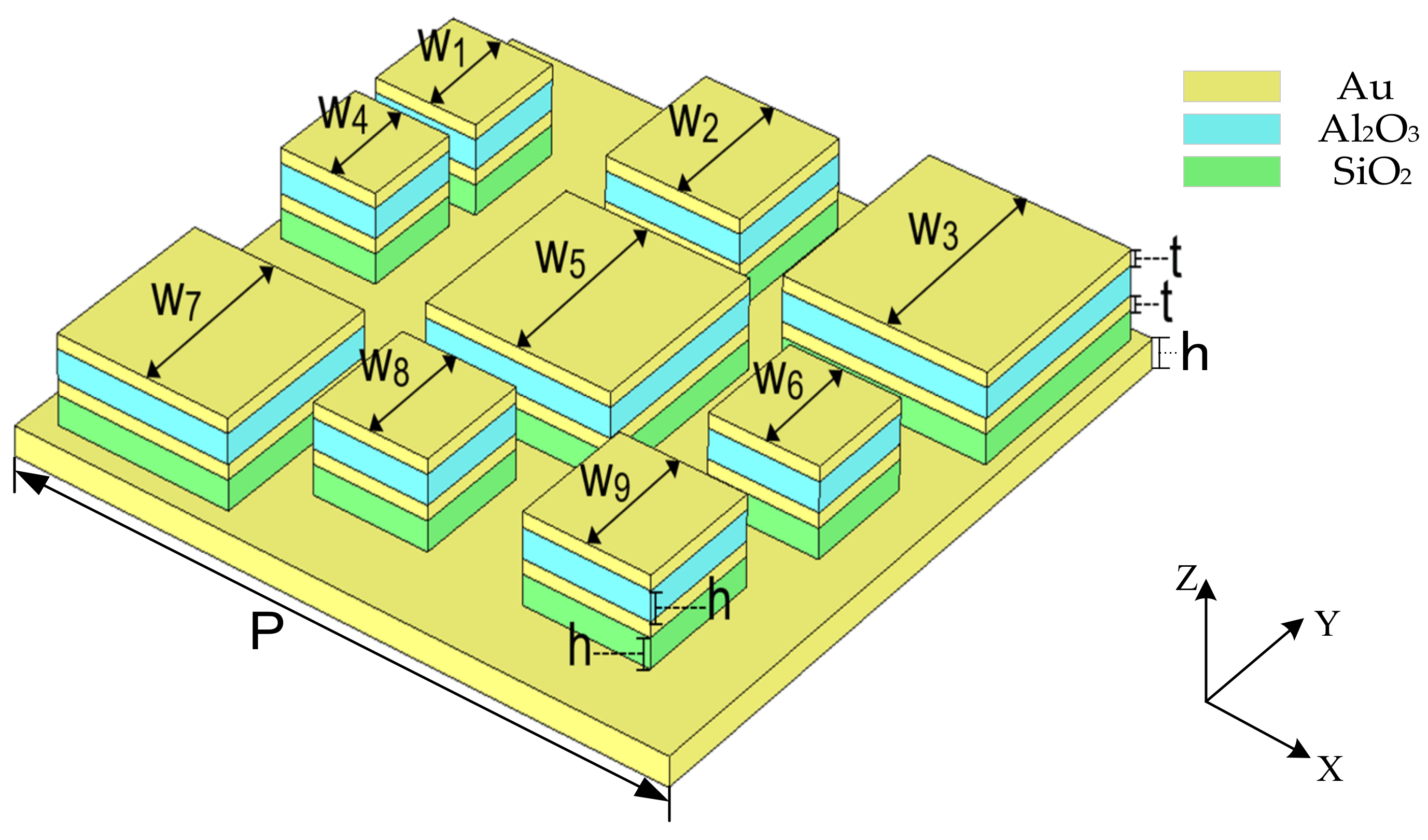
2. Design and Simulation

In Figure 1, we display the structure designed for the MA, which comprises nine square resonators of different sizes, consisting of four layers of Au, Al2O3, Au, and SiO2 placed on a square gold substrate, and we use the subscript w to indicate the sequence number of the resonators. Moreover, without considering the z-direction, we set the geometric center of the substrate as the coordinate origin; thus, the coordinates of resonator 1–9 center are (−4.7, 3.1), (−0.5, 4.0), (3.9, 3.9), (−4.8, 0.7), (0, 0), (4.1, −0.2), (−3.9, −4.0), (−0.5, 3.5), and (3.5, −3.5), respectively. The characteristics of the materials applied in the MA were the relative permittivity and loss tangent of Al2O3 and SiO2, and the conductivity of gold; the values of which are 2.28; 0.04, 3.9, and 0.025; and 4.56 × 10⁷ S/m, respectively. Additionally, we list the dimensions of the MA structural parameters in Table 1.
We carried out all the simulations using CST microwave studio 2020 software. We chose the frequency domain analyzer as the simulation solver to obtain the absorptivity of the MA with the simulation and calculation. The mesh type was tetrahedral. Further, in the x and y directions, we set the conditions of the boundary as the unit cell. Set as open add space, the condition of the boundary was applied in the direction of Zmax, while the boundary condition in the Zmin direction was set as grounding (Et = 0).

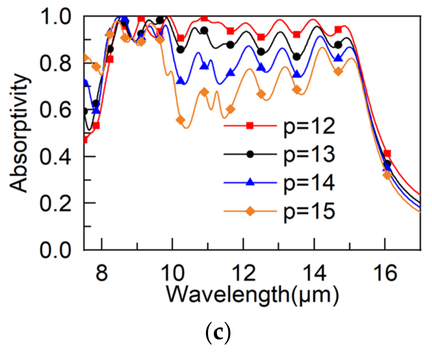
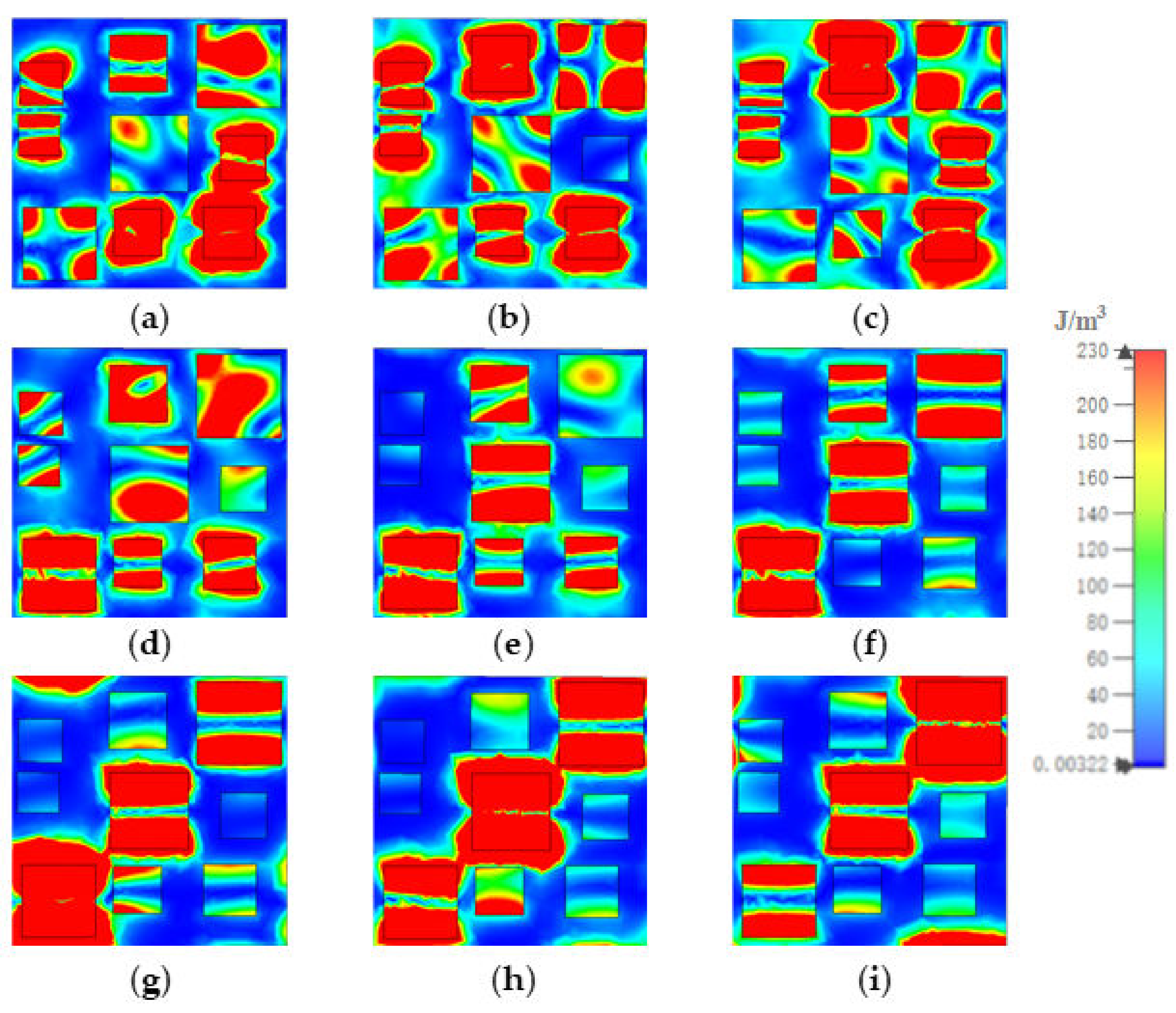
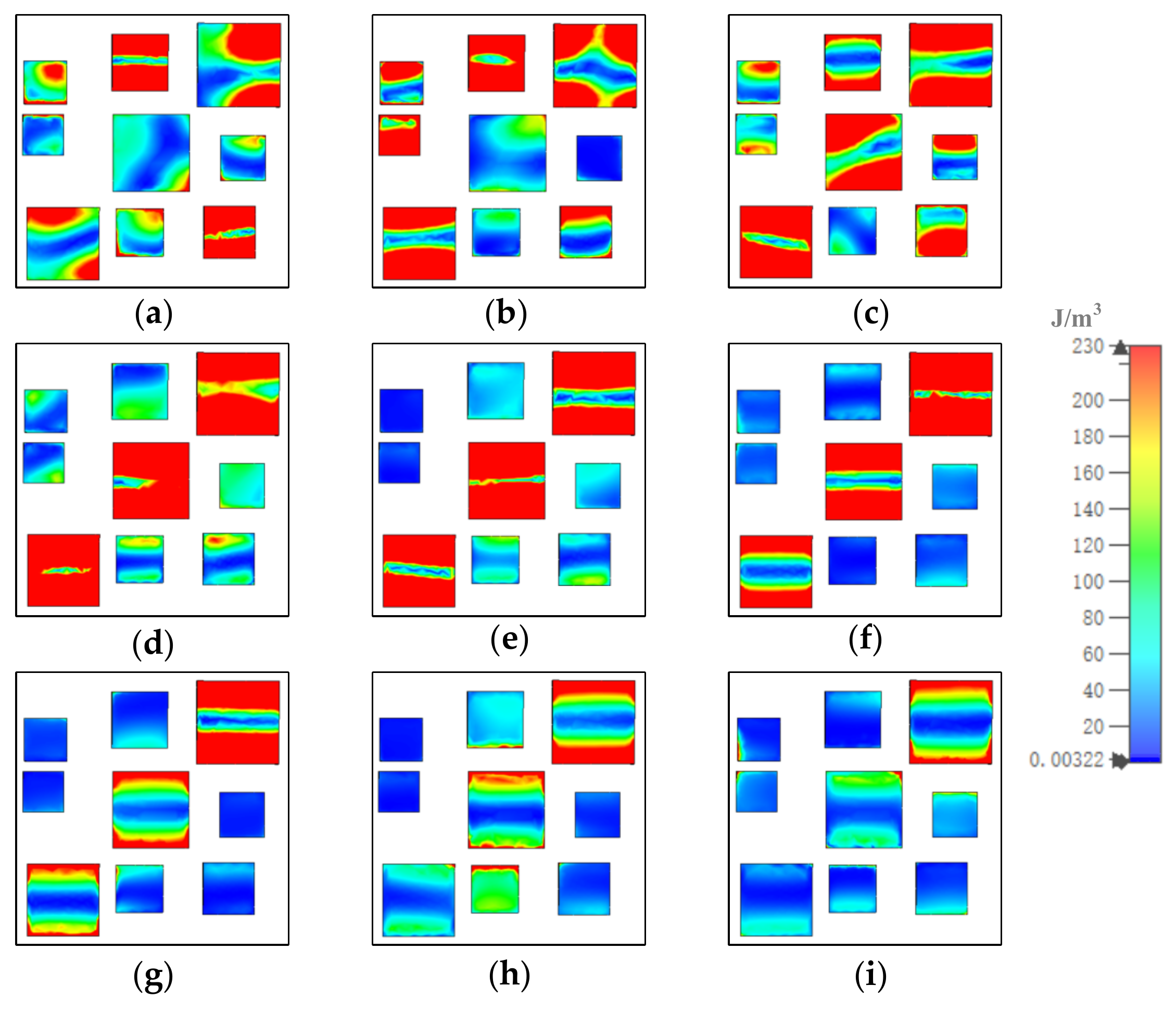
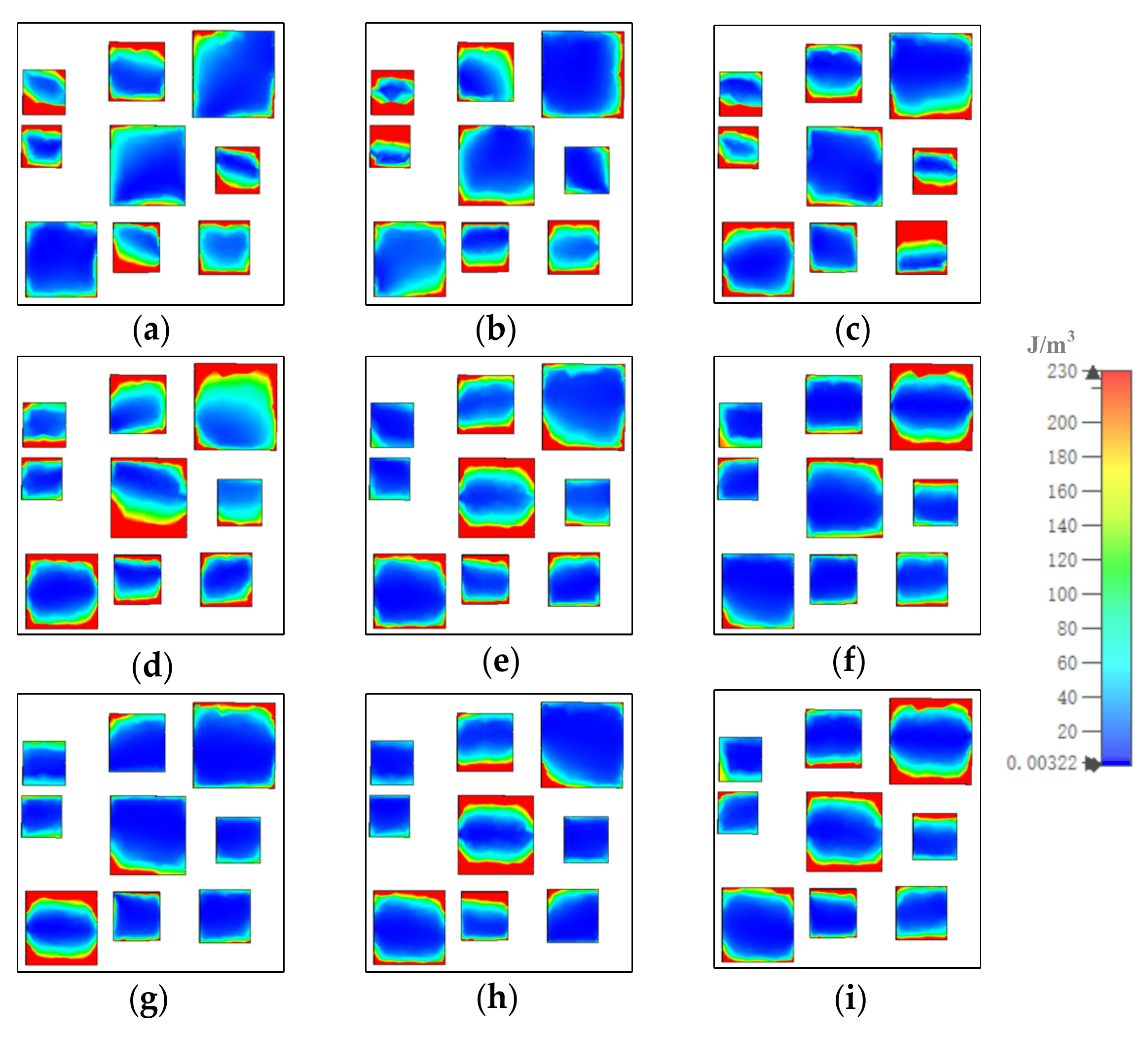
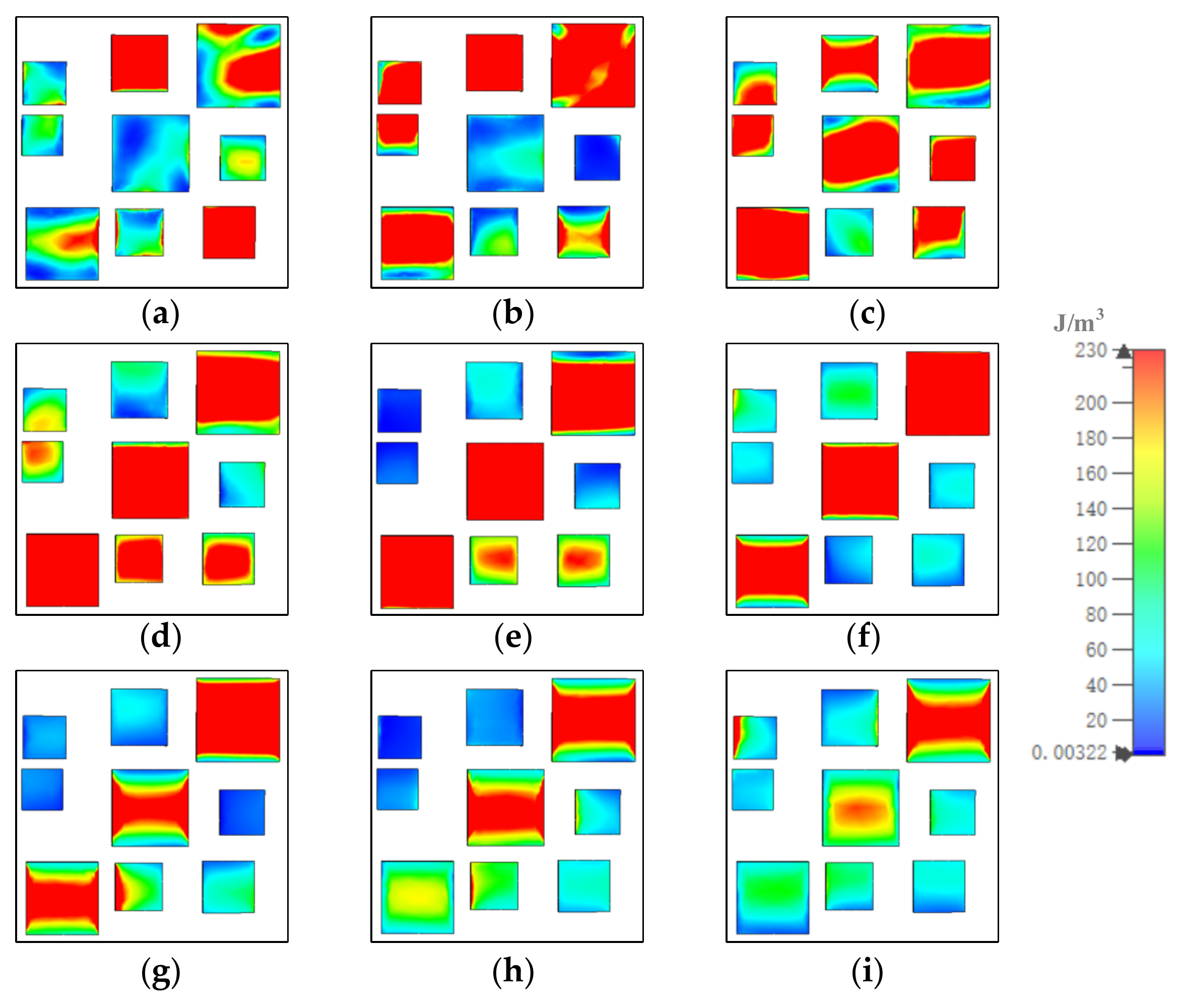
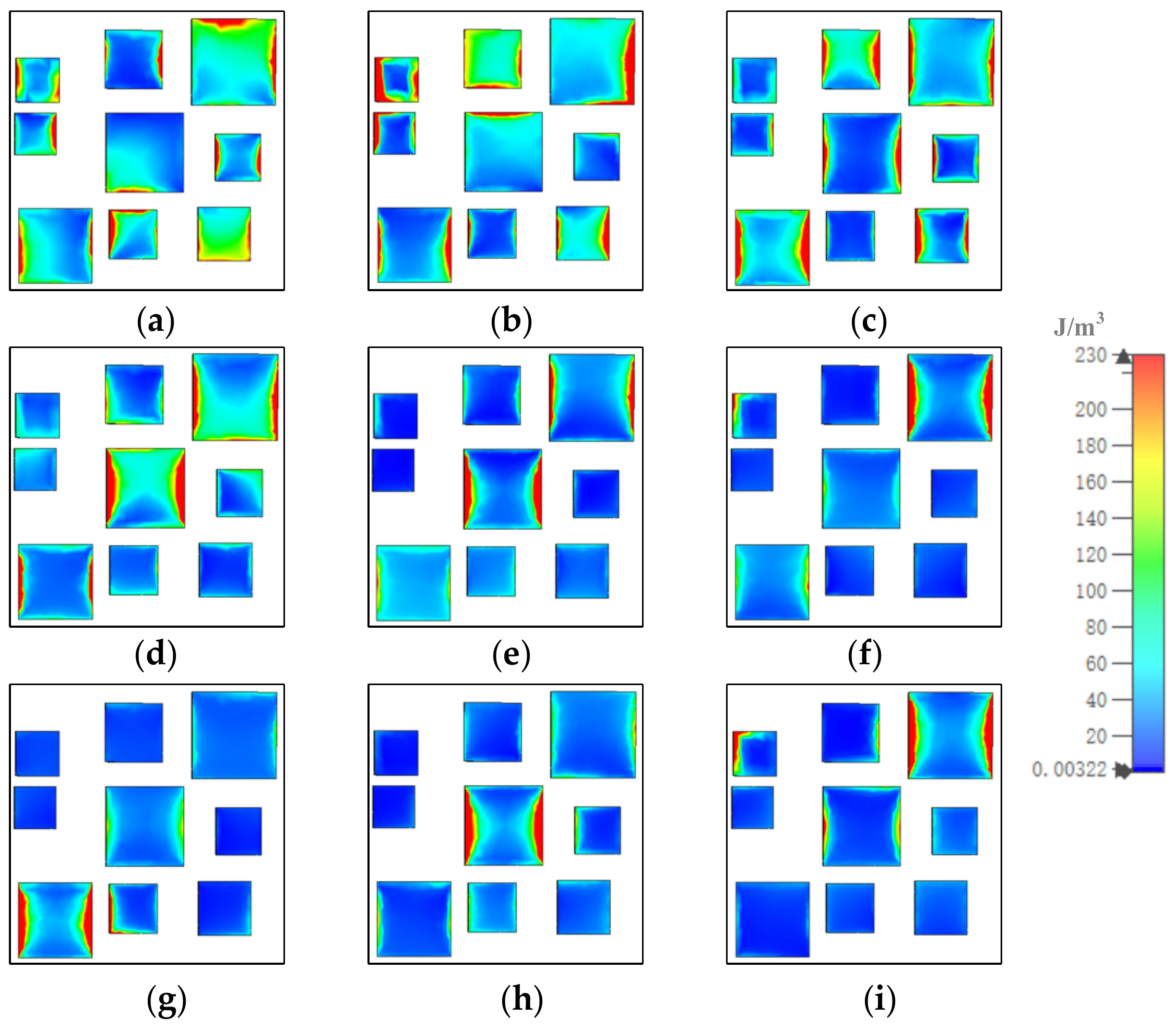
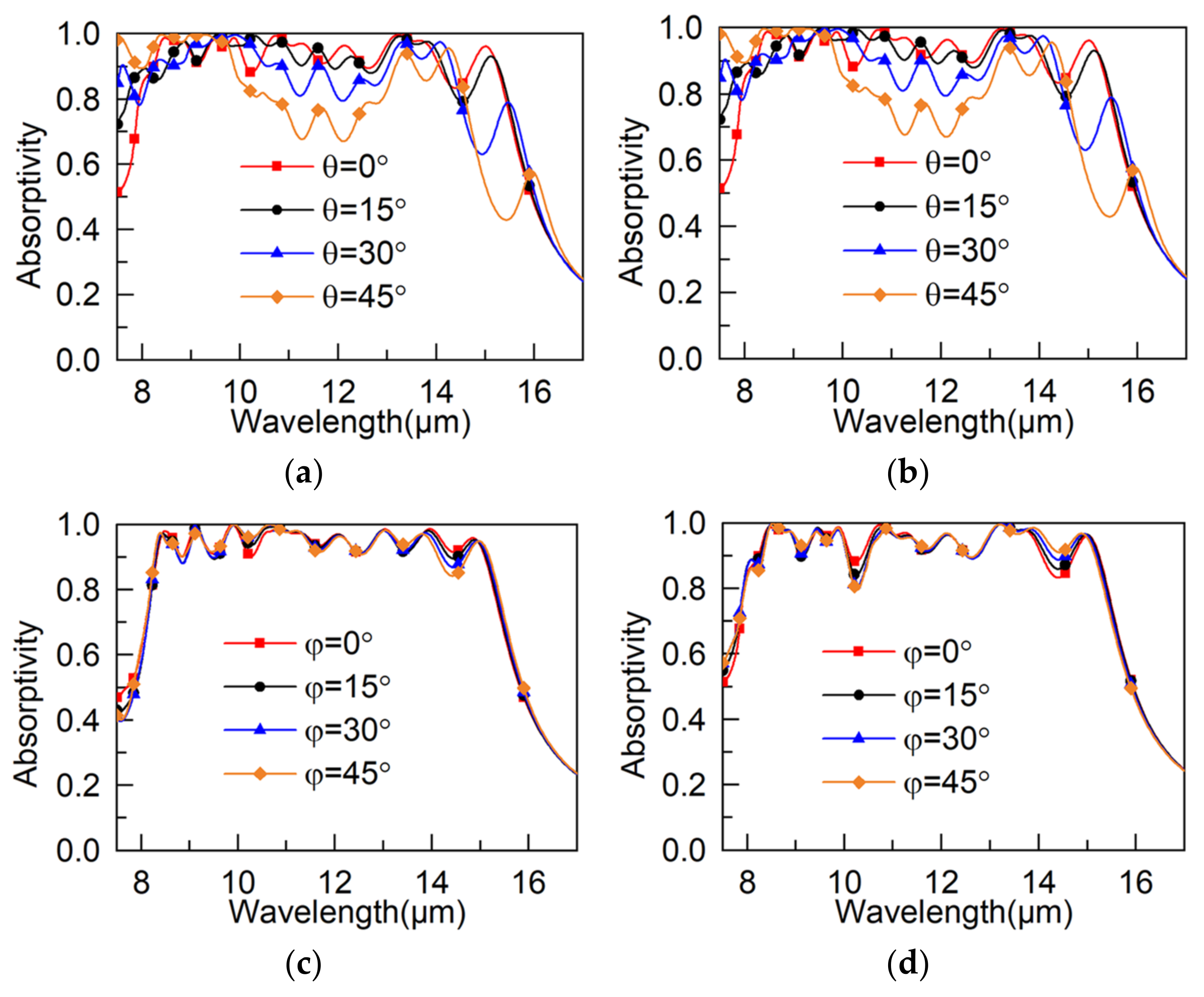
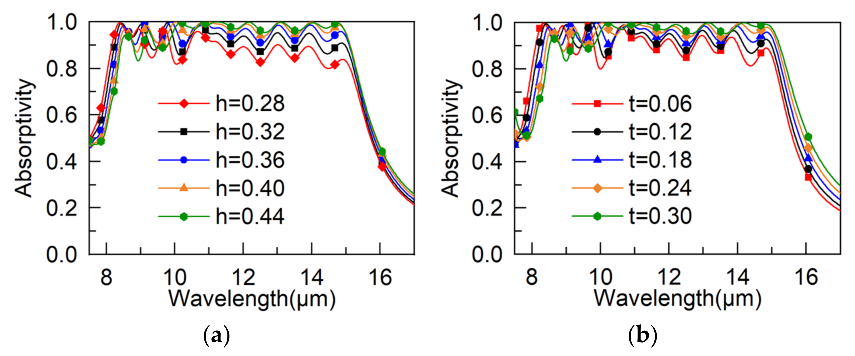
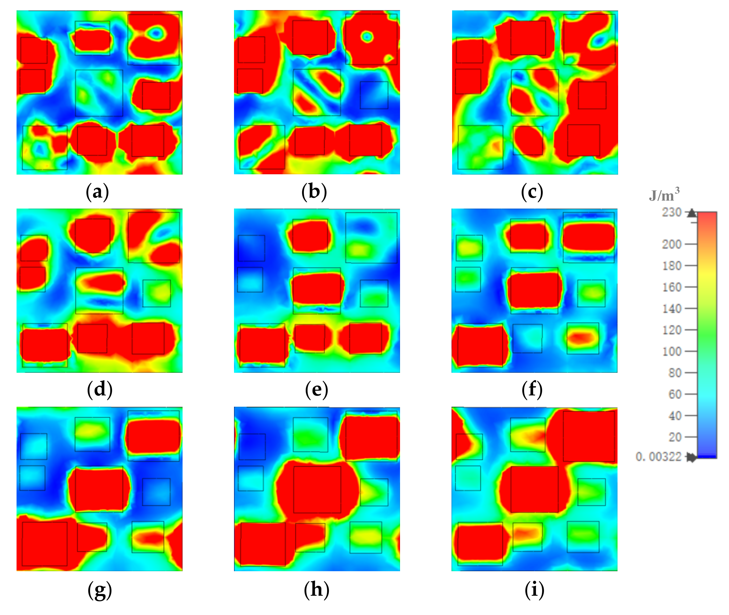
3. Results and Discussion

To calculate the absorptivity of the proposed MA, we used the equation A = 1 R T = 1 S 11 | 2 S 21 | 2 . In this equation, R and T represent the reflection ratio and transmission ratio, respectively, so that S 11 and S 21 represent the coefficient of reflection and transmission, respectively. In the range of mid-infrared, the gold substrate with thickness much thicker than skin depth caused the value of the transmission ratio for MA to be equal to zero. Therefore, the above equation can be further expressed as A = 1 R = 1 | S 11 | 2 .
The absorptivity of the MA is shown in Figure 2. In Figure 2a, the absorptivity under the transverse electric (TE) mode is greater than 0.9 in the 8.33–15.09 μm, and at the resonant peak of 9.88 μm, the absorptivity is over 99.9%. The performance of absorptivity under the Transverse Magnetic (TM) mode was not as good as under the TE mode due to the asymmetrical structure of the MA. Perfect absorption can be obtained when the equivalent impedance of MA and free space match. Hence, the performance of the proposed MA is explained by the equivalent impedance of the MA displayed in Figure 2b. As shown, at the resonant peaks of 8.5, 9.13, 9.88, 10.86, 11.26, 12.07, 13.03, 13.96, and 14.84 μm, the real and imaginary parts of the equivalent impedance for the proposed MA were nearly one and zero, respectively. Moreover, the equivalent impedance of the real and imaginary parts had a value around one and zero in the whole range of 8.33–15.09 μm, respectively. In summary, the proposed MA demonstrated perfect absorption because the equivalent impedance of the MA and corresponding value of the free space matched.
Investigating how the incidence and polarization affect the absorptivity, we further illustrated the performance of the proposed MA, and the results are displayed in Figure 3. In Figure 3a,b, compared with the results of a normal incident, we can see that under both the TE and TM modes, the performance of the MA was significantly worse with increasing incident angle because the resonance conditions can be changed with the obliquity of the incident wave. Meanwhile, Figure 3c,d show that the absorptivity changed across the whole operating frequency band with increasing polarization angle, which was a result of the non-central rotational symmetry structure of the MA.
We further simulated how the changes in the structure parameters affect the absorptivity, and the result is shown in Figure 4. In Figure 4a, we can see that the absorptivity is rising with increasing h when the wavelength is longer than 10.6 μm, and in the 8.33–10.6 μm range, the absorptivity of h = 0.36 μm shows the widest bandwidth. Figure 4b shows the relationship between absorptivity and the structure parameter t; when the wavelength is over 10.17 μm, there is a positive correlation between absorptivity and the value of t, while in the 8.33–10.17 μm range, the relationship is the opposite. Figure 4c shows that the structure period P has an obvious influence on the absorptivity. The performance of the MA deteriorates as the value of p becomes larger, and the minimum value of p is 12 μm due to the structure of the MA.
To investigate the distribution of the electric and magnetic fields, we analyzed the absorption mechanism of the MA. Figure 5, Figure 6, and Figure 7 show how the electric field energy distributed in each of the gold layers. At 8.5 μm, in gold substrate, most of the electric field energy distributed in the up and down sides under resonators 1, 2, 3, and 4; under resonator 7, the electric field energy distributed in four corners; and under resonators 6, 8, and 9, the electric field energy was almost fully covered. The distribution out of the range illustrated the coupling of resonators. In the middle gold layer, the electric field energy mainly distributed in the up and down sides of resonators 2, 3, and 9, and in several corners of resonators 1, 5, 6, 7, and 8. In the top gold layer, the electric field energy mainly distributed in the up and down sides of resonators 1, 2, 4, 6, 8, and 9. At other resonator points, the electric field energy distributions were similar to those at 8.5 μm, although the number and position of the resonator in which the most field energy distributes were different.
Figure 8, Figure 9 and Figure 10 show how the magnetic field energy distributed in each of the gold layers. At 8.5 μm, displayed in Figure 8, Figure 9 and Figure 10a, in gold substrate, most of the magnetic field energy distributed under resonators 1, 2, 3, 4, 6, 8, and 9. As shown, the magnetic field energy almost covered the whole space under resonators 1, 4, 6, 8, and 9. The distribution out of the range illustrated the coupling of resonators. In the middle gold layer, most of the magnetic energy distributed in the whole range of resonators 2 and 9, and large amounts of magnetic energy distributed in a horizontal stripe in the middle of resonators 3 and 7. In the top gold layer, the magnetic field energy mainly distributed in the left and right sides of resonators 1, 2, 3, 4, 6, 7, and 9. At other resonator points, the magnetic field energy distributions were similar to those at 8.5 μm, although the number and position of the resonator in which the most field energy distributes were different.
We concluded that most of the energy distributed in the gold substrate and middle gold layer, and the remaining minor electric field energy and magnetic field energy distributed in the up and down, and left and right sides of the resonator in the top gold layer, respectively. Not only the resonators but also the coupling of several resonators with different sizes contributed to the generation of the resonant peaks. Additionally, we present a comparison between the proposed MA and those reported in several previous works in Table 2, which illustrates the high performance of the proposed MA.

4. Conclusions

In summary, we proposed a metamaterial absorber characterized by ultra-broadband absorption in the mid-infrared range based on multi-sized resonators. Initially, we designed a 3 × 3 five-layer structure with Au, Al2O3, and SiO2 to absorb mid-infrared waves. Then, we changed the size of each resonator to expand the bandwidth because resonators with different sizes have different operation wavelengths and the relationship between them is positive. We further rearranged the resonators to change their distances, which created variation in the coupling condition between the resonators. Therefore, the performance of our MA was improved. By conducting simulations and calculations, we ensured the final design of the proposed MA. The results showed that the absorptivity of the proposed MA in the 8.33–15.09 μm waveband was higher than 90%, with an average absorptivity of 95.17%, and the absorption bandwidth was about 6.76 μm. The proposed MA has promising application value in the fields of infrared detection, infrared thermal energy utilization, radiation refrigeration, invisible camouflage, etc.

Author Contributions

Z.Z. and X.H. proposed the idea and conceived the design; Z.Z. carried out the simulation and wrote the original draft; M.C. and X.L. analyzed and discussed results; R.L. writing—review & editing and supervision; C.S. writing—review & editing and visualization. All authors have read and agreed to the published version of the manuscript.

Funding

This work was supported by the Project of Science and Technology of Shaanxi (2021JM-395).

Institutional Review Board Statement

Not applicable.

Informed Consent Statement

Not applicable.

Data Availability Statement

The data presented in this study are available on request from the corresponding author.

Conflicts of Interest

The authors declare no conflict of interest.

References

  1. Pendry, J.B.; Holden, A.J.; Stewart, W.J.; Youngs, I. Extremely Low Frequency Plasmons in Metallic Mesostructures. Phys. Rev. Lett. 1996, 76, 4773–4776. [Google Scholar] [CrossRef] [PubMed] [Green Version]
  2. Pendry, J.B.; Holden, A.J.; Robbins, D.J.; Stewart, W.J. Magnetism from conductors and enhanced nonlinear phenomena. IEEE Trans. Microw. Theory Tech. 1999, 47, 2075–2084. [Google Scholar] [CrossRef] [Green Version]
  3. Shelby, R.A.; Smith, D.R.; Schultz, S. Experimental Verification of a Negative Index of Refraction. Science 2001, 292, 77–79. [Google Scholar] [CrossRef] [PubMed] [Green Version]
  4. Wu, J.; Xie, Z.T.; Sha, Y.; Fu, H.; Li, Q. Epsilon-near-zero photonics: Infinite potentials. Photonics Res. 2021, 9, 1616. [Google Scholar] [CrossRef]
  5. Ye, W.; Zeuner, F.; Li, X.; Reineke, B.; He, S.; Qiu, C.-W.; Liu, J.; Wang, Y.; Zhang, S.; Zentgraf, T. Spin and wavelength multiplexed nonlinear metasurface holography. Nat. Commun. 2016, 7, 11930. [Google Scholar] [CrossRef] [PubMed]
  6. Zheng, G.; Mühlenbernd, H.; Kenney, M.; Li, G.; Zentgraf, T.; Zhang, S. Metasurface holograms reaching 80% efficiency. Nat. Nanotechnol. 2015, 10, 308–312. [Google Scholar] [CrossRef] [PubMed]
  7. Iwaszczuk, K.; Strikwerda, A.; Fan, K.; Zhang, X.; Averitt, R.D.; Jepsen, P.U. Flexible metamaterial absorbers for stealth applications at terahertz frequencies. Opt. Express 2011, 20, 635–643. [Google Scholar] [CrossRef] [Green Version]
  8. Qian, C.; Zheng, B.; Shen, Y.; Jing, L.; Li, E.; Shen, L.; Chen, H. Deep-learning-enabled self-adaptive microwave cloak without human intervention. Nat. Photonics 2020, 14, 383–390. [Google Scholar] [CrossRef]
  9. Balci, O.; Polat, E.O.; Kakenov, N.; Kocabas, C. Graphene-enabled electrically switchable radar-absorbing surfaces. Nat. Commun. 2015, 6, 6628. [Google Scholar] [CrossRef] [Green Version]
  10. Yilmaz, H.O.; Yaman, F. Metamaterial Antenna Designs for a 5.8-GHz Doppler Radar. IEEE Trans. Instrum. Meas. 2020, 69, 1775–1782. [Google Scholar] [CrossRef]
  11. Freitag, M.; Low, T.; Zhu, W.; Yan, H.; Xia, F.; Avouris, P. Photocurrent in graphene harnessed by tunable intrinsic plasmons. Nat. Commun. 2013, 4, 1951. [Google Scholar] [CrossRef] [Green Version]
  12. Lio, G.E.; Ferraro, A.; Giocondo, M.; Caputo, R.; De Luca, A. Color Gamut Behavior in Epsilon Near-Zero Nanocavities during Propagation of Gap Surface Plasmons. Adv. Opt. Mater. 2020, 8, 2000487. [Google Scholar] [CrossRef]
  13. Lio, G.; Ferraro, A. LIDAR and Beam Steering Tailored by Neuromorphic Metasurfaces Dipped in a Tunable Surrounding Medium. Photonics 2021, 8, 65. [Google Scholar] [CrossRef]
  14. Landy, N.I.; Sajuyigbe, S.; Mock, J.J.; Smith, D.R.; Padilla, W.J. Perfect Metamaterial Absorber. Phys. Rev. Lett. 2008, 100, 207402. [Google Scholar] [CrossRef]
  15. Shen, X.; Cui, T.J.; Zhao, J.; Ma, H.F.; Jiang, W.X.; Li, H. Polarization-independent wide-angle triple-band metamaterial absorber. Opt. Express 2011, 19, 9401–9407. [Google Scholar] [CrossRef]
  16. Andryieuski, A.; Lavrinenko, A. Graphene metamaterials based tunable terahertz absorber: Effective surface conductivity approach. Opt. Express 2013, 21, 9144–9155. [Google Scholar] [CrossRef] [Green Version]
  17. Zhao, X.; Wang, Y.; Schalch, J.; Duan, G.; Cremin, K.; Zhang, J.; Chen, C.; Averitt, R.D.; Zhang, X. Optically Modulated Ultra-Broadband All-Silicon Metamaterial Terahertz Absorbers. ACS Photonics 2019, 6, 830–837. [Google Scholar] [CrossRef]
  18. Wang, B.-X.; Xu, C.; Duan, G.; Jiang, J.; Xu, W.; Yang, Z.; Wu, Y. Miniaturized and Actively Tunable Triple-Band Terahertz Metamaterial Absorber Using an Analogy I-Typed Resonator. Nanoscale Res. Lett. 2022, 17, 35. [Google Scholar] [CrossRef]
  19. McCrindle, I.J.H.; Grant, J.; Drysdale, T.D.; Cumming, D.R.S. Multi-Spectral Materials: Hybridisation of Optical Plasmonic Filters and a Terahertz Metamaterial Absorber. Adv. Opt. Mater. 2013, 2, 149–153. [Google Scholar] [CrossRef] [Green Version]
  20. Xu, H.; Hu, L.; Lu, Y.; Xu, J.; Chen, Y. Dual-Band Metamaterial Absorbers in the Visible and Near-Infrared Regions. J. Phys. Chem. C 2019, 123, 10028–10033. [Google Scholar] [CrossRef]
  21. Yang, J.; Qu, S.; Ma, H.; Wang, J.; Yang, S.; Pang, Y. Broadband infrared metamaterial absorber based on anodic aluminum oxide template. Opt. Laser Technol. 2018, 101, 177–182. [Google Scholar] [CrossRef]
  22. Jung, J.-Y.; Lee, J.; Choi, J.-H.; Choi, D.-G.; Jeong, J.-H. Enhancement of refractive index sensing for infrared plasmonic metamaterial absorber with nanogap. Opt. Express 2021, 29, 22796–22804. [Google Scholar] [CrossRef]
  23. Liu, J.; Ma, W.-Z.; Chen, W.; Yu, G.-X.; Chen, Y.-S.; Deng, X.-C.; Yang, C.-F. Numerical analysis of an ultra-wideband metamaterial absorber with high absorptivity from visible light to near-infrared. Opt. Express 2020, 28, 23748. [Google Scholar] [CrossRef] [PubMed]
  24. Baqir, M.A.; Choudhury, P.K. Hyperbolic Metamaterial-Based UV Absorber. IEEE Photonics Technol. Lett. 2017, 29, 1548–1551. [Google Scholar] [CrossRef]
  25. Liu, X.; Ren, Z.; Yang, T.; Chen, L.; Wang, Q.; Zhou, J. Tunable metamaterial absorber based on resonant strontium titanate artificial atoms. J. Mater. Sci. Technol. 2020, 62, 249–253. [Google Scholar] [CrossRef]
  26. Luo, Z.; Ji, S.; Zhao, J.; Wu, H.; Dai, H. A multiband metamaterial absorber for GHz and THz simultaneously. Results Phys. 2021, 30, 104893. [Google Scholar] [CrossRef]
  27. Tofigh, F.; Amiri, M.; Shariati, N.; Lipman, J.; Abolhasan, M. Polarization-Insensitive Metamaterial Absorber for Crowd Estimation Based on Electromagnetic Energy Measurements. IEEE Trans. Antennas Propag. 2019, 68, 1458–1467. [Google Scholar] [CrossRef]
  28. Qian, J.; Zhou, J.; Zhu, Z.; Ge, Z.; Wu, S.; Liu, X.; Yi, J. Polarization-Insensitive Broadband THz Absorber Based on Circular Graphene Patches. Nanomaterials 2021, 11, 2709. [Google Scholar] [CrossRef]
  29. Cheng, Y.Z.; Cheng, Z.Z.; Mao, X.S.; Gong, R.Z. Ultra-Thin Multi-Band Polarization-Insensitive Microwave Metamaterial Absorber Based on Multiple-Order Responses Using a Single Resonator Structure. Materials 2017, 10, 1241. [Google Scholar] [CrossRef] [Green Version]
  30. Huang, X.; Yang, H.; Shen, Z.; Chen, J.; Lin, H.; Yu, Z. Water-injected all-dielectric ultra-wideband and prominent oblique incidence metamaterial absorber in microwave regime. J. Phys. D Appl. Phys. 2017, 50, 385304. [Google Scholar] [CrossRef]
  31. Shabanpour, J.; Beyraghi, S.; Oraizi, H. Reconfigurable honeycomb metamaterial absorber having incident angular stability. Sci. Rep. 2020, 10, 14920. [Google Scholar] [CrossRef]
  32. Li, J.; Li, J.; Zhou, H.; Zhang, G.; Liu, H.; Wang, S.; Yi, F. Plasmonic metamaterial absorbers with strong coupling effects for small pixel infrared detectors. Opt. Express 2021, 29, 22907–22921. [Google Scholar] [CrossRef]
  33. Huang, X.; Cao, M.; Wang, D.; Li, X.; Fan, J.; Li, X. Broadband polarization-insensitive and oblique-incidence terahertz metamaterial absorber with multi-layered graphene. Opt. Mater. Express 2022, 12, 811. [Google Scholar] [CrossRef]
  34. Feng, R.; Qiu, J.; Liu, L.; Ding, W.; Chen, L. Parallel LC circuit model for multi-band absorption and preliminary design of radiative cooling. Opt. Express 2014, 22, A1713–A1724. [Google Scholar] [CrossRef]
  35. Zhou, Y.; Liang, Z.; Qin, Z.; Shi, X.; Meng, D.; Zhang, L. Results in Physics Broadband Long Wavelength Infrared Metamaterial Absorbers. Results Phys. 2020, 19, 103566. [Google Scholar] [CrossRef]
  36. Guo, W.; Liu, Y.; Han, T. Ultra-broadband infrared metasurface absorber. Opt. Express 2016, 24, 20586–20592. [Google Scholar] [CrossRef]
  37. Qin, Z.; Shi, X.; Yang, F.; Hou, E.; Meng, D.; Sun, C.; Dai, R.; Zhang, S.; Liu, H.; Xu, H.; et al. Multi-mode plasmonic resonance broadband LWIR metamaterial absorber based on lossy metal ring. Opt. Express 2021, 30, 473. [Google Scholar] [CrossRef]
  38. Zhou, Y.; Liang, Z.; Qin, Z.; Hou, E.; Shi, X.; Zhang, Y.; Xiong, Y.; Tang, Y.; Fan, Y.; Yang, F.; et al. Small-Sized Long Wavelength Infrared Absorber with Perfect Ultra-Broadband Absorptivity. Opt. Express 2020, 28, 1279–1290. [Google Scholar] [CrossRef]
  39. Wu, B.; Liu, Z.; Du, G.; Chen, Q.; Liu, X.; Fu, G.; Liu, G. Polarization and angle insensitive ultra-broadband mid-infrared perfect absorber. Phys. Lett. A 2020, 384, 126288. [Google Scholar] [CrossRef]
  40. Ozbay, I.; Ghobadi, A.; Butun, B.; Turhan-Sayan, G. Bismuth plasmonics for extraordinary light absorption in deep sub-wavelength geometries. Opt. Lett. 2020, 45, 686–689. [Google Scholar] [CrossRef]
  41. Tang, Y.; Meng, D.; Liang, Z.; Qin, Z.; Shi, X.; Zhang, Y.; Xiong, Y.; Fan, Y.; Yang, F.; Zhang, L.; et al. An Infrared Metamaterial Broadband Absorber Based on a Simple Titanium Disk with High Absorption and a Tunable Spectral Absorption Band. Ann. Phys. 2020, 532, 2000145. [Google Scholar] [CrossRef]
  42. Qin, Z.; Meng, D.; Yang, F.; Shi, X.; Liang, Z.; Xu, H.; Smith, D.R.; Liu, Y. Broadband long-wave infrared metamaterial absorber based on single-sized cut-wire resonators. Opt. Express 2021, 29, 20275–20285. [Google Scholar] [CrossRef] [PubMed]
Figure 1. Schematic view of the Au, Al2O3, Au, SiO2, and Au 3 × 3 five-layer unit cell.
Materials 15 05411 g001
Figure 2. (a) Absorptivity of the MA; (b) real and imaginary parts of equivalent impedance of the MA.
Materials 15 05411 g002
Figure 3. Absorptivity with (a) oblique incident of TE wave, (b) oblique incident of TM wave, (c) different polarization angles of TE wave, and (d) different polarization angles of TM wave.
Materials 15 05411 g003
Figure 4. Absorptivity with different (a) thickness of dielectric layers, (b) thickness of gold layers, and (c) period geometry.
Materials 15 05411 g004aMaterials 15 05411 g004b
Figure 5. The distribution of electric field energy in gold substrate at (a) 8.5, (b) 9.13, (c) 9.88, (d) 10.86, (e) 11.26, (f) 12.07, (g) 13.03, (h) 13.96, and (i) 14.84 μm.
Materials 15 05411 g005
Figure 6. The distribution of electric field energy in middle gold layer at (a) 8.5, (b) 9.13, (c) 9.88, (d) 10.86, (e) 11.26, (f) 12.07, (g) 13.03, (h) 13.96, and (i) 14.84 μm.
Materials 15 05411 g006
Figure 7. The distribution of electric field energy in top gold layer at (a) 8.5, (b) 9.13, (c) 9.88, (d) 10.86, (e) 11.26, (f) 12.07, (g) 13.03, (h) 13.96, and (i) 14.84 μm.
Materials 15 05411 g007
Figure 8. The distribution of magnetic field energy in gold substrate at (a) 8.5, (b) 9.13, (c) 9.88, (d) 10.86, (e) 11.26, (f) 12.07, (g) 13.03, (h) 13.96, and (i) 14.84 μm.
Materials 15 05411 g008
Figure 9. The distribution of magnetic field energy in middle gold layer at (a) 8.5, (b) 9.13, (c) 9.88, (d) 10.86, (e) 11.26, (f) 12.07, (g) 13.03, (h) 13.96, and (i) 14.84 μm.
Materials 15 05411 g009
Figure 10. The distribution of magnetic field energy in top gold layer at (a) 8.5, (b) 9.13, (c) 9.88, (d) 10.86, (e) 11.26, (f) 12.07, (g) 13.03, (h) 13.96, and (i) 14.84 μm.
Materials 15 05411 g010
Table 1. Dimension of the MA structural parameters.
ParameterSize (μm)ParameterSize (μm)
P12w41.8
t0.18w53.4
h0.36w62.0
w11.9w73.2
w22.5w82.1
w33.7w92.3
Table 2. Comparison between proposed MA and those designed in previous works.
ReferenceOperation BandwidthRelative BandwidthAverage Absorptivity
[37]7.76–14 μm57.35%93.8%
[38]8–14 μm54.54%94.5%
[41]8–12 μm40%92.1%
[42]7.5–13.25 μm55.42%91.7%
Proposed MA8.33–15.09 μm57.73%95.17%
Publisher’s Note: MDPI stays neutral with regard to jurisdictional claims in published maps and institutional affiliations.

