
Influence of the Electron Beam and the Choice of Heating Membrane on the Evolution of Si Nanowires’ Morphology in In Situ TEM

 , and
, and 
Abstract
:1. Introduction
2. Experiments
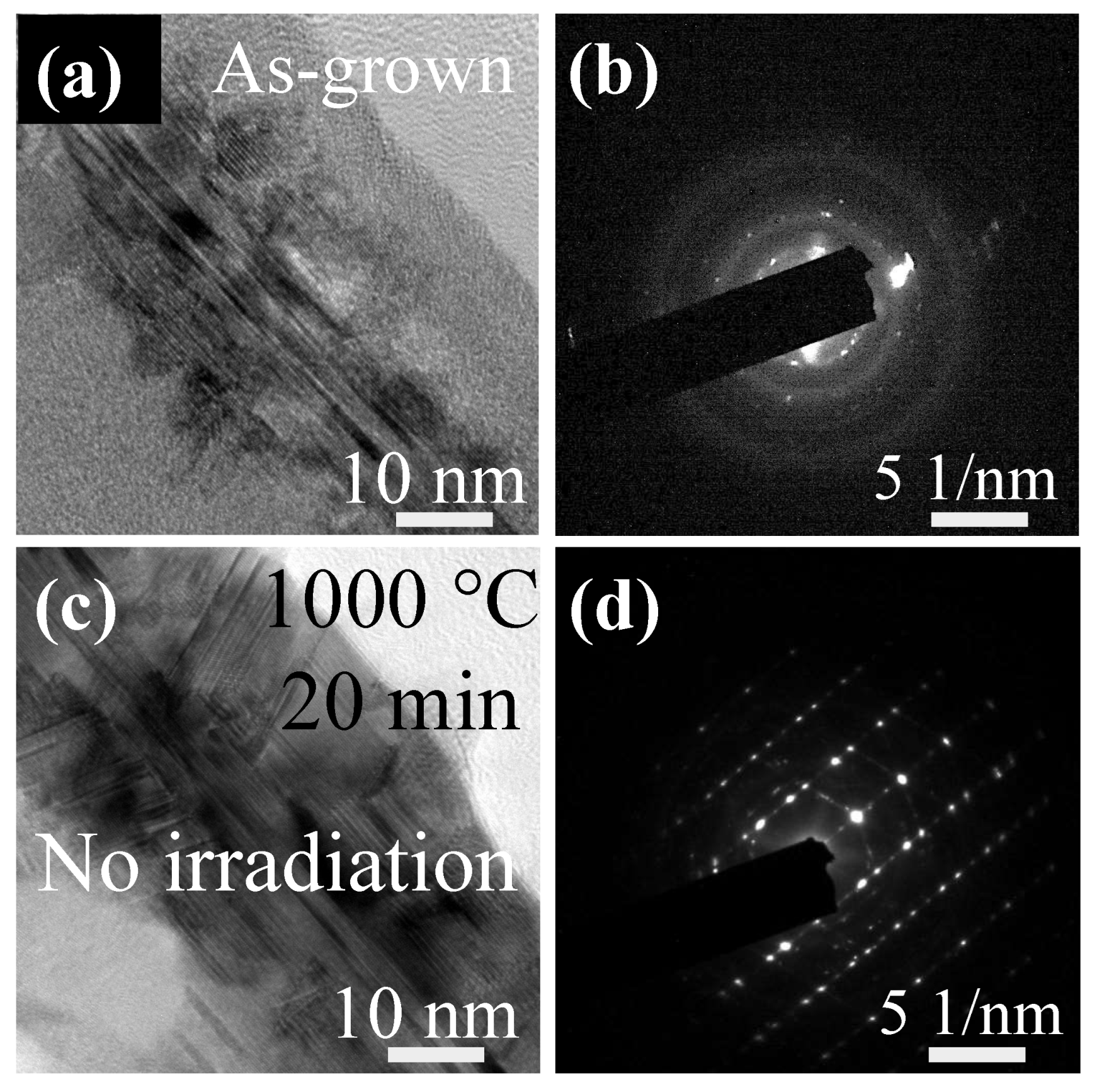
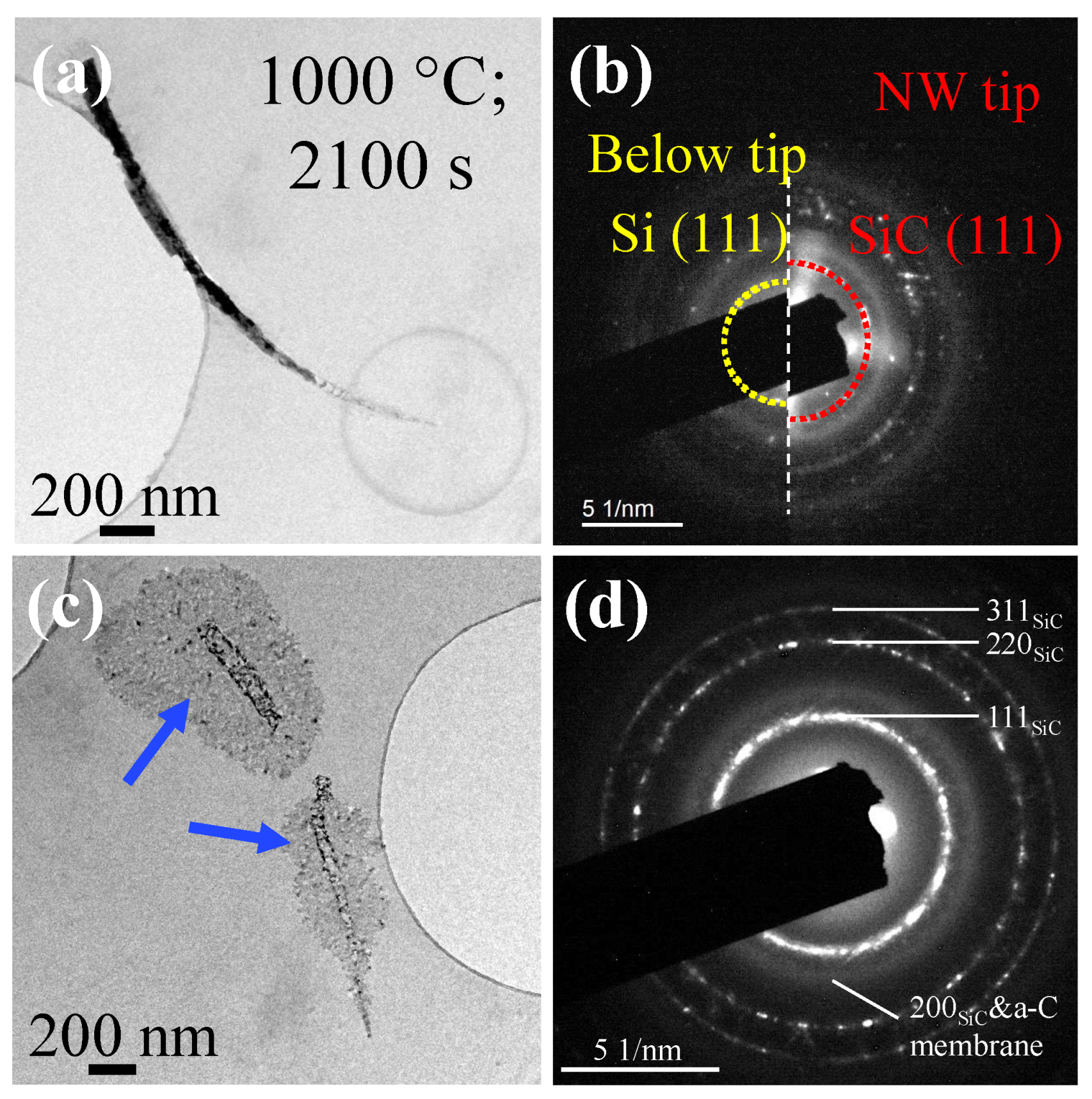
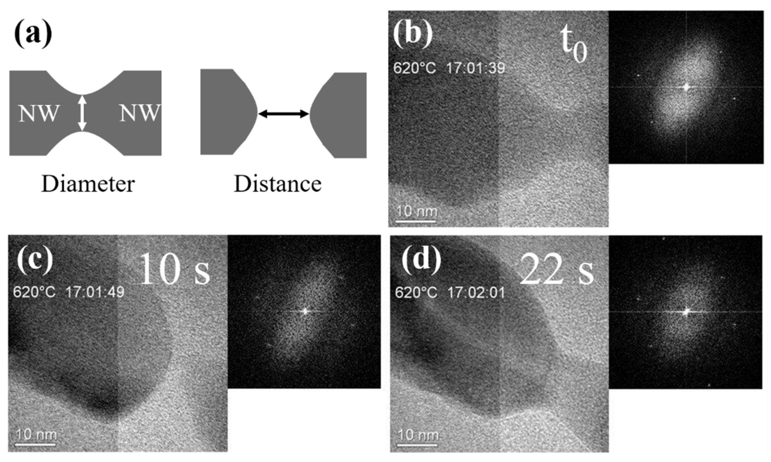
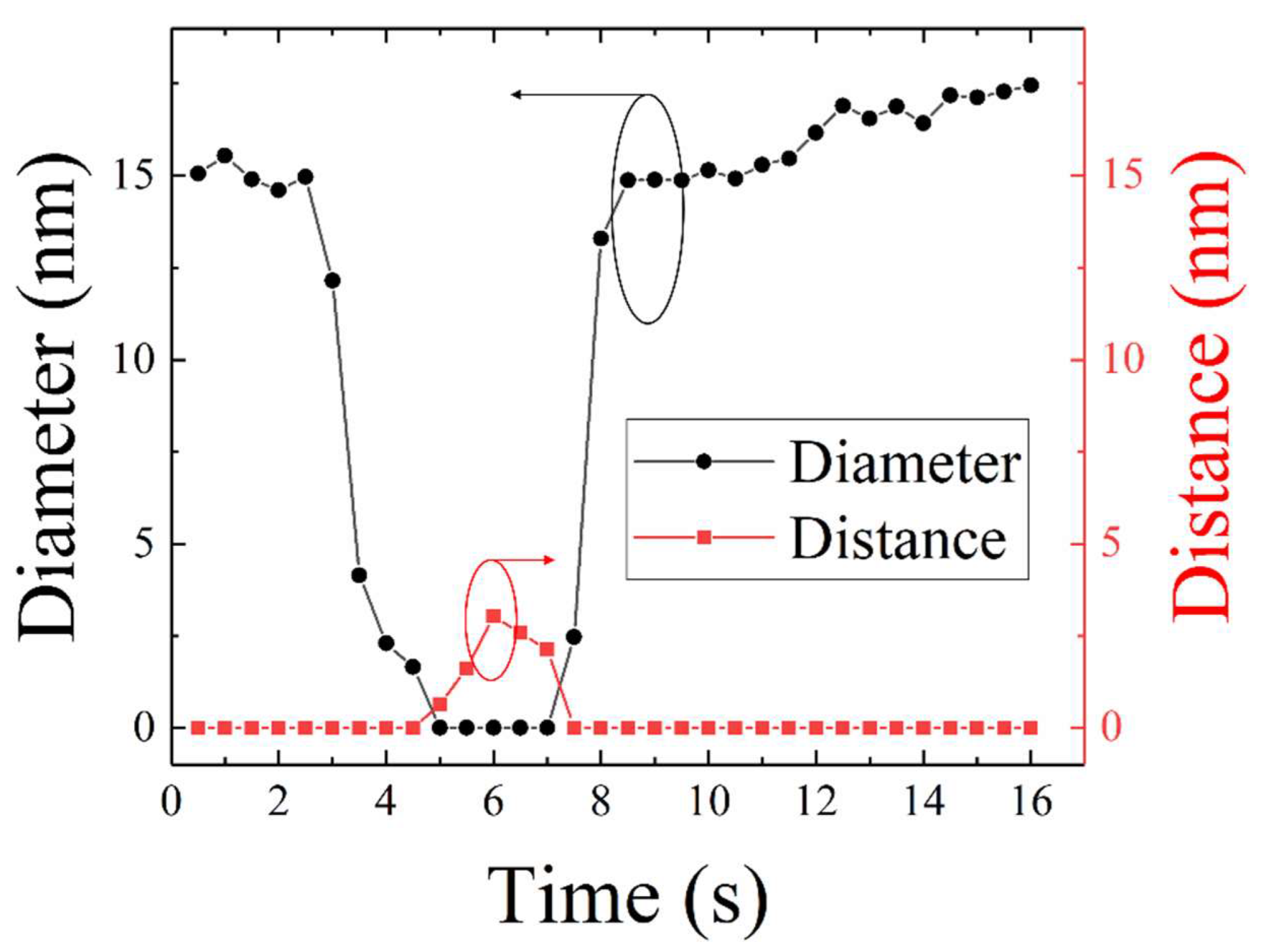
3. Results and Discussion
4. Conclusions
Supplementary Materials
Author Contributions
Funding
Institutional Review Board Statement
Informed Consent Statement
Data Availability Statement
Acknowledgments
Conflicts of Interest
References
- Chen, W.; Yu, L.; Misra, S.; Fan, Z.; Pareige, P.; Patriarche, G.; Bouchoule, S.; Roca i Cabarrocas, P. Incorporation and redistribution of impurities into silicon nanowires during metal-particle-assisted growth. Nat. Commun. 2014, 5, 4134. [Google Scholar] [CrossRef] [PubMed]
- Chen, W.; Pareige, P.; Roca i Cabarrocas, P. Three-dimensional atomic mapping of hydrogenated polymorphous silicon solar cells. Appl. Phys. Lett. 2016, 108, 253110. [Google Scholar] [CrossRef]
- Saka, H.; Kamino, T.; Ara, S.; Sasaki, K. In situ heating transmission electron microscopy. MRS Bull. 2008, 33, 93–100. [Google Scholar] [CrossRef]
- Zhang, Z.; Su, D. Behaviour of TEM metal grids during in-situ heating experiments. Ultramicroscopy 2009, 109, 766–774. [Google Scholar] [CrossRef] [Green Version]
- Chen, L.; Liu, J.; Jiang, C.; Zhao, K.; Chen, H.; Shi, X.; Chen, L.; Sun, C.; Zhang, S.; Wang, Y.; et al. Nanoscale Behavior and Manipulation of the Phase Transition in Single-Crystal Cu2Se. Adv. Mater. 2019, 31, 1804919. [Google Scholar] [CrossRef]
- Asano, S.; Engel, B.D.; Baumeister, W. In situ cryo-electron tomography: A post-reductionist approach to structural biology. J. Mol. Biol. 2016, 428, 332–343. [Google Scholar] [CrossRef] [Green Version]
- McDowall, A.; Smith, J.; Dubochet, J. Cryo-electron microscopy of vitrified chromosomes in situ. EMBO J. 1986, 5, 1395–1402. [Google Scholar] [CrossRef] [PubMed]
- Wu, J.; Shan, H.; Chen, W.; Gu, X.; Tao, P.; Song, C.; Shang, W.; Deng, T. In situ environmental TEM in imaging gas and liquid phase chemical reactions for materials research. Adv. Mater. 2016, 28, 9686–9712. [Google Scholar] [CrossRef]
- Wagner, J.B.; Cavalca, F.; Damsgaard, C.D.; Duchstein, L.D.; Hansen, T.W. Exploring the environmental transmission electron microscope. Micron 2012, 43, 1169–1175. [Google Scholar] [CrossRef] [PubMed] [Green Version]
- Yuan, W.; Zhu, B.; Fang, K.; Li, X.-Y.; Hansen Thomas, W.; Ou, Y.; Yang, H.; Wagner Jakob, B.; Gao, Y.; Wang, Y.; et al. In situ manipulation of the active Au-TiO2 interface with atomic precision during CO oxidation. Science 2021, 371, 517–521. [Google Scholar] [CrossRef]
- Yuan, W.; Zhu, B.; Li, X.-Y.; Hansen Thomas, W.; Ou, Y.; Fang, K.; Yang, H.; Zhang, Z.; Wagner Jakob, B.; Gao, Y.; et al. Visualizing H2O molecules reacting at TiO2 active sites with transmission electron microscopy. Science 2020, 367, 428–430. [Google Scholar] [CrossRef] [PubMed]
- Ma, Z.; Sheng, L.; Wang, X.; Yuan, W.; Chen, S.; Xue, W.; Han, G.; Zhang, Z.; Yang, H.; Lu, Y.; et al. Oxide Catalysts with Ultrastrong Resistance to SO2 Deactivation for Removing Nitric Oxide at Low Temperature. Adv. Mater. 2019, 31, 1903719. [Google Scholar] [CrossRef] [PubMed]
- Le Ferrand, H.; Duchamp, M.; Gabryelczyk, B.; Cai, H.; Miserez, A. Time-resolved observations of liquid–liquid phase separation at the nanoscale using in situ liquid transmission electron microscopy. J. Am. Chem. Soc. 2019, 141, 7202–7210. [Google Scholar] [CrossRef] [PubMed]
- Evans, J.E.; Jungjohann, K.L.; Wong, P.C.; Chiu, P.-L.; Dutrow, G.H.; Arslan, I.; Browning, N.D. Visualizing macromolecular complexes with in situ liquid scanning transmission electron microscopy. Micron 2012, 43, 1085–1090. [Google Scholar] [CrossRef]
- Minor, A.M.; Dehm, G. Advances in in situ nanomechanical testing. MRS Bull. 2019, 44, 438–442. [Google Scholar] [CrossRef] [Green Version]
- Boston, R.; Schnepp, Z.; Nemoto, Y.; Sakka, Y.; Hall, S.R. In situ TEM observation of a microcrucible mechanism of nanowire growth. Science 2014, 344, 623–626. [Google Scholar] [CrossRef]
- Petkov, N. In Situ Real-Time TEM Reveals Growth, Transformation and Function in One-Dimensional Nanoscale Materials: From a Nanotechnology Perspective. ISRN Nanotechnol. 2013, 2013, 893060. [Google Scholar] [CrossRef] [Green Version]
- Kim, J.H.; Kim, J.G.; Song, J.; Bae, T.-S.; Kim, K.-H.; Lee, Y.-S.; Pang, Y.; Oh, K.H.; Chung, H.-S. Investigation of the growth and in situ heating transmission electron microscopy analysis of Ag2S-catalyzed ZnS nanowires. Appl. Surf. Sci. 2018, 436, 556–561. [Google Scholar] [CrossRef]
- Panciera, F.; Norton, M.M.; Alam, S.B.; Hofmann, S.; Mølhave, K.; Ross, F.M. Controlling nanowire growth through electric field-induced deformation of the catalyst droplet. Nat. Commun. 2016, 7, 12271. [Google Scholar] [CrossRef] [Green Version]
- Li, J.; Leonard Deepak, F. In situ generation of sub-10 nm silver nanowires under electron beam irradiation in a TEM. Chem. Commun. 2020, 56, 4765–4768. [Google Scholar] [CrossRef]
- Wen, C.-Y.; Reuter, M.; Bruley, J.; Tersoff, J.; Kodambaka, S.; Stach, E.; Ross, F. Formation of compositionally abrupt axial heterojunctions in silicon-germanium nanowires. Science 2009, 326, 1247–1250. [Google Scholar] [CrossRef] [PubMed] [Green Version]
- Alam, S.B.; Andersen, C.R.; Panciera, F.; Nilausen, A.A.; Hansen, O.; Ross, F.M.; Mølhave, K. In situ TEM modification of individual silicon nanowires and their charge transport mechanisms. Nanotechnology 2020, 31, 494002. [Google Scholar] [CrossRef]
- Panciera, F.; Baraissov, Z.; Patriarche, G.; Dubrovskii, V.G.; Glas, F.; Travers, L.; Mirsaidov, U.; Harmand, J.-C. Phase selection in self-catalyzed GaAs nanowires. Nano Lett. 2020, 20, 1669–1675. [Google Scholar] [CrossRef]
- Zobelli, A.; Gloter, A.; Ewels, C.; Colliex, C. Shaping single walled nanotubes with an electron beam. Phys. Rev. B 2008, 77, 045410. [Google Scholar] [CrossRef] [Green Version]
- Kohno, H.; Mori, Y.; Ichikawa, S.; Ohno, Y.; Yonenaga, I.; Takeda, S. Transformation of a SiC nanowire into a carbon nanotube. Nanoscale 2009, 1, 344–346. [Google Scholar] [CrossRef]
- Ting, Y.-H.; Wu, M.-C.; Aoyama, Y.; Lu, K.-C.; Wu, W.-W. In situ manipulation of E-beam irradiation-induced nanopore formation on molybdenum oxide nanowires. Appl. Surf. Sci. 2021, 544, 148874. [Google Scholar] [CrossRef]
- Harmand, J.-C.; Patriarche, G.; Glas, F.; Panciera, F.; Florea, I.; Maurice, J.-L.; Travers, L.; Ollivier, Y. Atomic step flow on a nanofacet. Phys. Rev. Lett. 2018, 121, 166101. [Google Scholar] [CrossRef]
- Yuan, W.; Yu, J.; Li, H.; Zhang, Z.; Sun, C.; Wang, Y. In situ TEM observation of dissolution and regrowth dynamics of MoO2 nanowires under oxygen. Nano Res. 2016, 10, 397–404. [Google Scholar] [CrossRef]
- Qin, Q.; Yin, S.; Cheng, G.; Li, X.; Chang, T.-H.; Richter, G.; Zhu, Y.; Gao, H. Recoverable plasticity in penta-twinned metallic nanowires governed by dislocation nucleation and retraction. Nat. Commun. 2015, 6, 5983. [Google Scholar] [CrossRef] [PubMed] [Green Version]
- Sarkar, R.; Rentenberger, C.; Rajagopalan, J. Electron Beam Induced Artifacts During in situ TEM Deformation of Nanostructured Metals. Sci. Rep. 2015, 5, 16345. [Google Scholar] [CrossRef] [Green Version]
- Yamasaki, J.; Takeda, S.; Tsuda, K. Elemental process of amorphization induced by electron irradiation in Si. Phys. Rev. B 2002, 65, 115213. [Google Scholar] [CrossRef]
- Teweldebrhan, D.; Balandin, A. A Modification of graphene properties due to electron-beam irradiation. Appl. Phys. Lett. 2009, 94, 021912. [Google Scholar] [CrossRef] [Green Version]
- Bae, I.-T.; Zhang, Y.; Weber, W.J.; Higuchi, M.; Giannuzzi, L. A Electron-beam induced recrystallization in amorphous apatite. Appl. Phys. Lett. 2007, 90, 021912. [Google Scholar] [CrossRef]
- Casu, A.; Lamberti, A.; Stassi, S.; Falqui, A. Crystallization of TiO2 nanotubes by in situ heating TEM. Nanomaterials 2018, 8, 40. [Google Scholar] [CrossRef] [Green Version]
- Kamins, T.; Li, X.; Williams, R.S.; Liu, X. Growth and structure of chemically vapor deposited Ge nanowires on Si substrates. Nano Lett. 2004, 4, 503–506. [Google Scholar] [CrossRef]
- Luce, F.P.; Oliviero, E.; Azevedo, G.D.M.; Baptista, D.L.; Zawislak, F.C.; Fichtner, P.F.P. In-situ transmission electron microscopy growth of nanoparticles under extreme conditions. J. Appl. Phys. 2016, 119, 035901. [Google Scholar] [CrossRef]
- Mohapatra, S. In-Situ TEM Observation of Electron Irradiation Induced Shape Transition of Elongated Gold Nanoparticles Embedded In Silica. Adv. Mater. Lett. 2013, 4, 444–448. [Google Scholar] [CrossRef]
- Nanda, K.K. On the paradoxical relation between the melting temperature and forbidden energy gap of nanoparticles. J. Chem. Phys. 2010, 133, 054502. [Google Scholar] [CrossRef] [PubMed]
- Misra, S.; Yu, L.; Chen, W.; Roca i Cabarrocas, P. Wetting Layer: The Key Player in Plasma-Assisted Silicon Nanowire Growth Mediated by Tin. J. Phys. Chem. C 2013, 117, 17786–17790. [Google Scholar] [CrossRef]
- Rodríguez-Manzo, J.A.; Terrones, M.; Terrones, H.; Kroto, H.W.; Sun, L.; Banhart, F. In situ nucleation of carbon nanotubes by the injection of carbon atoms into metal particles. Nat. Nanotechnol. 2007, 2, 307–311. [Google Scholar] [CrossRef] [PubMed]
- Egerton, R.F.; Li, P.; Malac, M. Radiation damage in the TEM and SEM. Micron 2004, 35, 399–409. [Google Scholar] [CrossRef] [PubMed]
- Le, D.N.; Nguyen-Truong, H.T. Analytical Formula for the Electron Inelastic Mean Free Path. J. Phys. Chem. C 2021, 125, 18946–18951. [Google Scholar] [CrossRef]
- Wilson, G.; Dennison, J.R. Approximation of Range in Materials as a Function of Incident Electron Energy. IEEE Trans. Plasma Sci. 2012, 40, 291–297. [Google Scholar] [CrossRef]
- Sikora, T.; Serin, V. 2008 The EELS Spectrum Database; Luysberg, M., Tillmann, K., Weirich, T., Eds.; Springer: Berlin/Heidelberg, Germany, 2008; pp. 439–440. [Google Scholar]
- Weber, L.; Gmelin, E. Transport properties of silicon. Appl. Phys. A 1991, 53, 136–140. [Google Scholar] [CrossRef]
- Egerton, R.; McLeod, R.; Wang, F.; Malac, M. Basic questions related to electron-induced sputtering in the TEM. Ultramicroscopy 2010, 110, 991–997. [Google Scholar] [CrossRef]

Publisher’s Note: MDPI stays neutral with regard to jurisdictional claims in published maps and institutional affiliations. |
© 2022 by the authors. Licensee MDPI, Basel, Switzerland. This article is an open access article distributed under the terms and conditions of the Creative Commons Attribution (CC BY) license (https://creativecommons.org/licenses/by/4.0/).
Share and Cite
Shen, Y.; Zhao, X.; Gong, R.; Ngo, E.; Maurice, J.-L.; Roca i Cabarrocas, P.; Chen, W. Influence of the Electron Beam and the Choice of Heating Membrane on the Evolution of Si Nanowires’ Morphology in In Situ TEM. Materials 2022, 15, 5244. https://doi.org/10.3390/ma15155244
Shen Y, Zhao X, Gong R, Ngo E, Maurice J-L, Roca i Cabarrocas P, Chen W. Influence of the Electron Beam and the Choice of Heating Membrane on the Evolution of Si Nanowires’ Morphology in In Situ TEM. Materials. 2022; 15(15):5244. https://doi.org/10.3390/ma15155244
Chicago/Turabian StyleShen, Ya, Xuechun Zhao, Ruiling Gong, Eric Ngo, Jean-Luc Maurice, Pere Roca i Cabarrocas, and Wanghua Chen. 2022. "Influence of the Electron Beam and the Choice of Heating Membrane on the Evolution of Si Nanowires’ Morphology in In Situ TEM" Materials 15, no. 15: 5244. https://doi.org/10.3390/ma15155244
APA StyleShen, Y., Zhao, X., Gong, R., Ngo, E., Maurice, J.-L., Roca i Cabarrocas, P., & Chen, W. (2022). Influence of the Electron Beam and the Choice of Heating Membrane on the Evolution of Si Nanowires’ Morphology in In Situ TEM. Materials, 15(15), 5244. https://doi.org/10.3390/ma15155244