Article

Applied IrO2 Buffer Layer as a Great Promoter on Ti-Doping V2O5 Electrode to Enhance Electrochromic Device Properties

1
Department of Mechanical Engineering, National Taiwan University, Taipei City 10617, Taiwan
2
Division of Physics, Institute of Nuclear Energy Research, Taoyuan City 32546, Taiwan
*
Authors to whom correspondence should be addressed.
Materials 2022, 15(15), 5179; https://doi.org/10.3390/ma15155179
Submission received: 24 June 2022 / Revised: 18 July 2022 / Accepted: 19 July 2022 / Published: 26 July 2022
(This article belongs to the Special Issue Preparation and Properties of Thin Films)

Abstract

:
Electrochromic devices (ECDs) are a promising material for smart windows that are capable of transmittance variation. However, ECDs are still too expensive to achieve a wide market reach. Reducing fabrication cost remains a challenge. In this study, we inserted an IrO2 buffer layer on Ti-doped V2O5 (Ti:V2O5) as a counter electrode using various Ar/O2 gas flow ratios (1/2, 1/2.5, 1/3 and 1/3.5) in the fabrication process. The buffered-ECD resulted in a larger cyclic voltammetry (CV) area and the best surface average roughness (Ra = 3.91 nm) to promote electrochromic performance. It was fabricated using the low-cost, fast deposition process of vacuum cathodic arc plasma (CAP). This study investigates the influence of the IrO2 buffer/Ti:V2O5 electrode on ECD electrochemical and optical properties, in terms of color efficiency (CE) and cycle durability. The buffered ECD (glass/ITO/WO3/liquid electrolyte/IrO2 buffer/Ti:V2O5/ITO/glass) demonstrated excellent optical transmittance modulation; ∆T = 57% (from Tbleaching (67%) to Tcoloring (10%)) at 633 nm, which was higher than without the buffer (ITO/WO3/liquid electrolyte/Ti:V2O5/ITO) (∆T = 36%). In addition, by means of an IrO2 buffer, the ECD exhibited high coloration efficiency of 96.1 cm2/mC and good durability, which decayed by only 2% after 1000 cycles.

1. Introduction

As part of the drive to mitigate the global energy crisis, one approach is the development of energy saving devices. Electrochromic devices (ECDs) are regarded as excellent candidates for research, as they feature low power usage, reversible changing, low-power drives large optical modulation, and good memory [1,2,3,4]. ECDs are attracting considerable attention since they have practical applications in smart windows for buildings and in heat-insulating glass for airplanes [5,6].
Smart windows are based on electrochromic materials that block solar and indoor sunlight and heat, enabling a reduction in the energy required for air conditioning [7]. A wide variety of ECD materials have been studied, including transition metal oxides, such as nickel oxide (NiO), tungsten oxide (WO3), zinc oxide (ZnO), and vanadium oxide (V2O5) [8,9,10,11].
WO3 is a well-known cathodic material and NiO is a common anodic material [12,13,14]. The main drawbacks of the NiO ECDs are the low contrast in optical transmittance and short durability [15,16]. Hence, V2O5 film has recently been studied as an anodic electrode in ECD, where it can participate in reversible oxidation and reduction reactions, which facilitate the movement of Li ions into/out of the interface electrodes and electrolyte [17,18]. The typical redox reaction of V2O5 with perchlorate (LiClO4) electrolyte can be written as follows [19]:
V2O5 + xLi+ + x = LixV2O5
Many studies have reported that V2O5 with appropriate dopants, such as Mn, Ag, Al, and Ti [20,21,22,23], can improve the microstructure electrochemical characteristics. The effect of Li+ reversibility on Ti-doped V2O5 (Ti:V2O5) is particularly interesting [24] and Kumar et al. indicate that the proper ratio of Ti added to V2O5 could increase the charge density as well as promote the cycling stability [23]. Here, we report an approach that inserts an IrO2 buffer layer on the Ti:V2O5 counter electrode to significantly enhance the high coloration efficiency and optical modulation contrast. The superior performance is ascribed to the buffer layer, which is beneficial for the electrode used in forming ECDs, as it results in prominent durability. The findings show that the buffer layer can enhance the properties of ECDs.
In general, ECD electrode films comprise an anode and a cathode and can be manufactured by several methods, including sputtering [25,26,27], chemical deposition [28,29], sol–gel [30,31], dip coating [32,33], pulsed-laser deposition [34], and electrodeposition [35]. Sputtering is the most common technology for electrode film preparation. In this work, the Ti:V2O5 and WO3 electrodes with the IrO2 buffer layer were fabricated using cathodic arc plasma (CAP). This technique has the advantages of high-density plasma that significantly promotes deposition rate, low cost, good film thickness control, a growing porous structure to benefit electrochromism, and is capable of achieving substrate deposition over a larger area without using complicated machinery. However, the CAP technique is not widely applied owing to poorer macroparticle production. This is caused by the effect of the plasma–liquid pool on cathode spots, attaching to the electrode film and making the performance inferior. The harmful macroparticles are the main reason why the CAP technique is not suitable for industrial application. Therefore, we developed a method that made use of Thornton deposition [36,37] to reduce macroparticle size and adjust the process parameters for high-pressure work to produce a self-organized structure, with a high horizontal magnetic field to improve the quality.
In this study, we inserted a buffer into the ECD structure between the liquid electrolyte and the Ti:V2O5 counter electrode. The structure is a multiple layer sandwich consisting of a pair of transparent conducting oxides (TCOs), a working electrochromic electrode (WO3), and a counter electrode (Ti:V2O5) in a perchlorate (LiClO4/PC) liquid electrolyte solution. Throughout the entire study, we found that the IrO2 buffer layer was indispensable for the electrochemical properties and optical contrast of ECDs. Buffered-ECDs were comparable to without-Buffered ECDs that were well-equipped with durability through prolonged long cycles. We have developed the CAP technique as an alternative method to deposit film, due to its high deposition rate, low processing costs, and ability to coat a large area substrate. The above process advantages are beneficial for the application of ECDs in green window construction. Furthermore, our goal is to make affordable ECD products. Recently, our research group, P.W. Chen et al. [7], reported a method to fabricate complementary electrochromic devices on WO3/NO electrodes, and discussed the influence of different WO3 film thicknesses on ECDs.
The elaboration of an IrO2 buffer layer on various Ar/O2 gas flow ratio parameters of the Ti:V2O5 counter electrode by the CAP technique is presented. This buffer is deposited on a good interfacial Ti:V2O5 electrode film based on the optimized Ar/O2 gas flow ratio that exhibited the best roughness of amorphous structure and cycle voltammetry (CV), providing a larger enveloped area with sufficient movement of Li ions in/out of the electrode. The configurations of the buffer ECD are illustrated in Figure 1. We investigated the effects of inserting an IrO2 buffer layer between a Ti:V2O5 electrode and an electrolyte, to gain insight into the impact of the buffer on the ECD. Our intent in this approach led to notable mechanical behavior, making the IrO2 buffer a potential candidate material for improving ECDs. The influence of an IrO2 buffer layer, based on the optimal CV measurements, optical transmittance, and surface roughness, on the Ti:V2O5 electrode film on the material crystallinity, surface morphology, coloration efficiency, and cycle durability are investigated in this work. We determined that the buffer is a very important layer in the ECD and serves many functions.

2. Materials and Methods

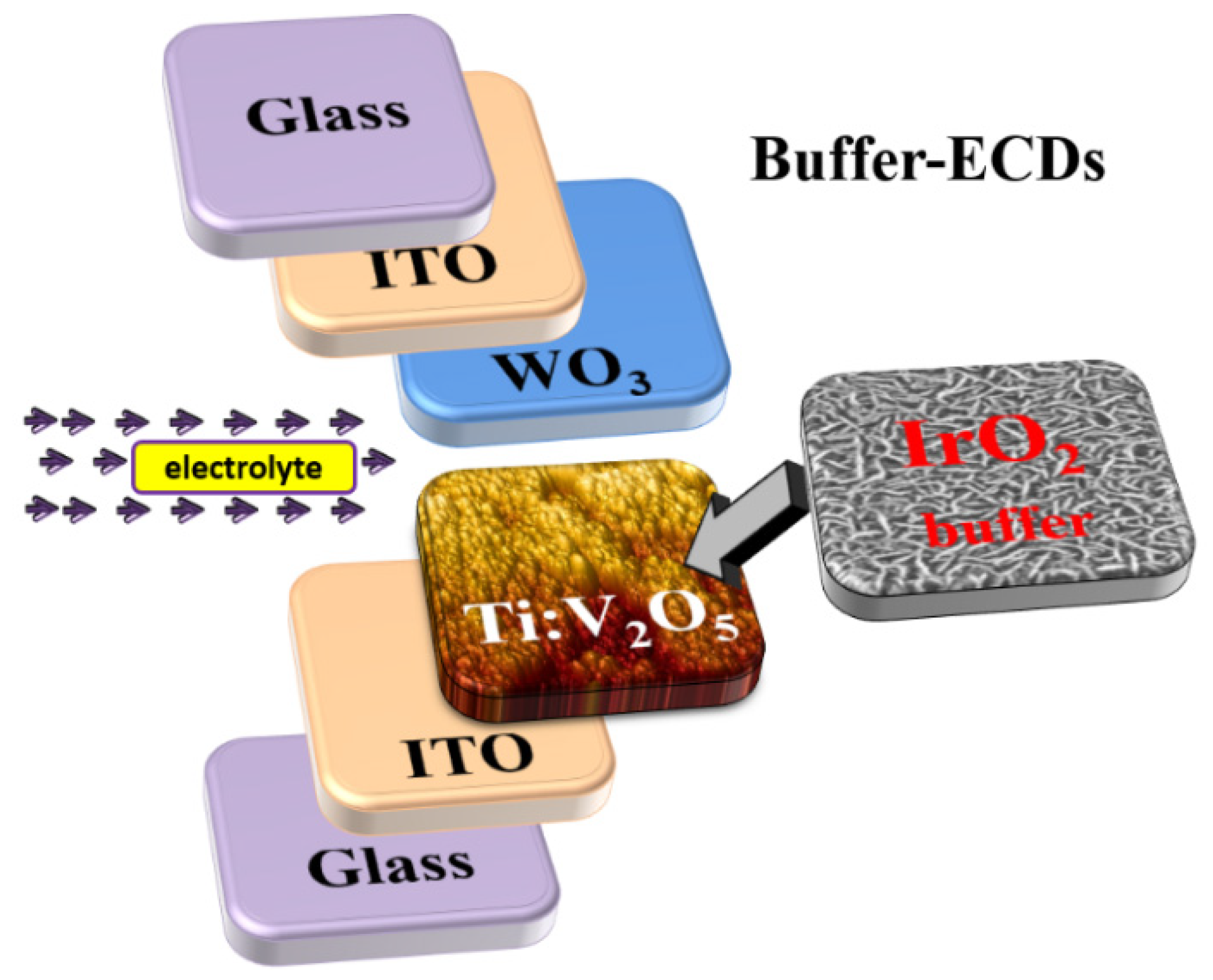
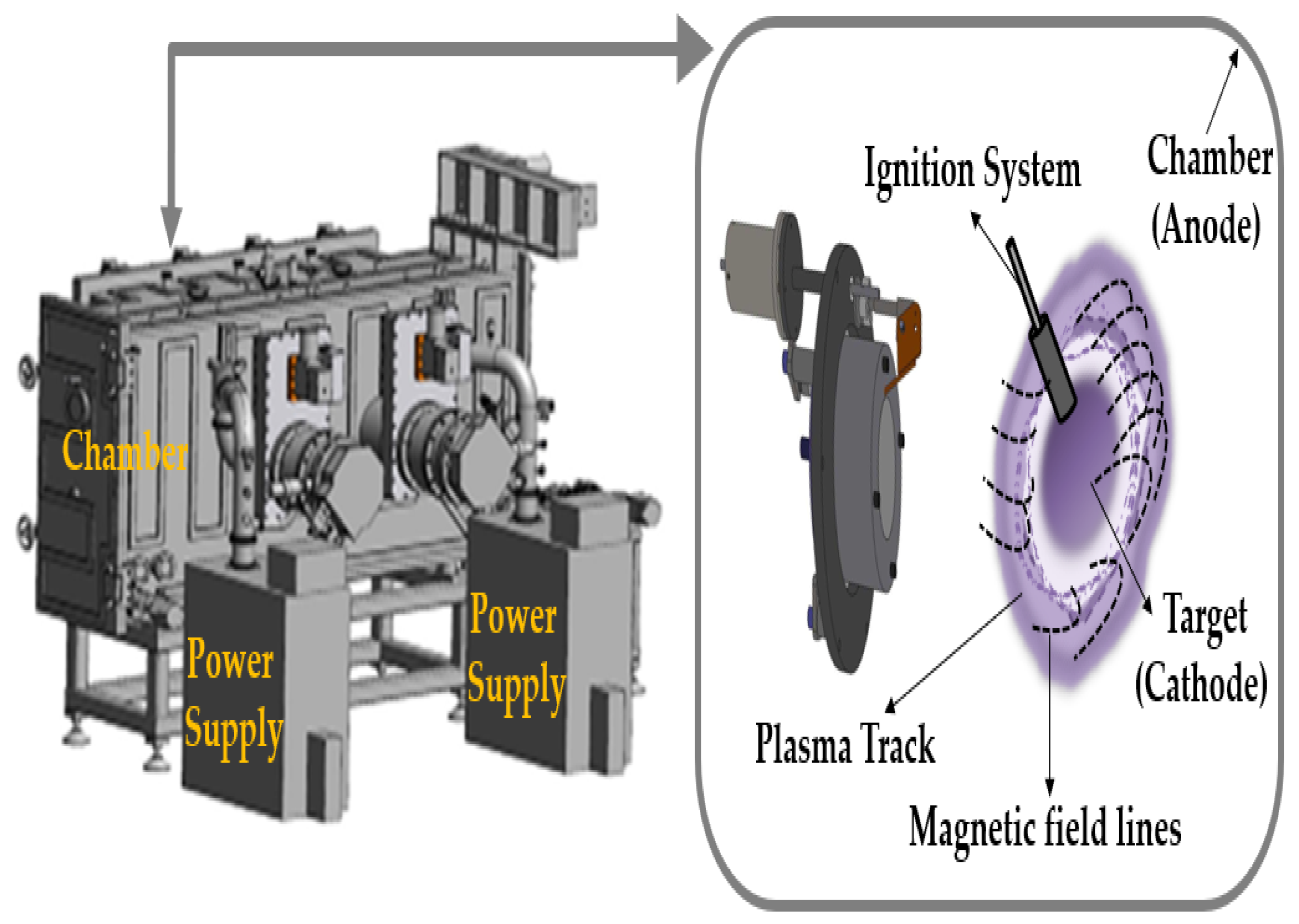
2.1. Deposition of Ti:V2O5 Counter Electrode and IrO2 Buffer Layer

The Ti:V2O5 electrode and IrO2 buffer layer were fabricated by the CAP technique showing in Figure 2 and using the targets of Ti-doped V2O5 (Ti:V = 1:2; 99.95% purity) and metallic iridium (Ir) target (99.95% purity), respectively. We deposited the Ti:V2O5 films (samples 1–4) using a series of reaction Ar/O2 gas flow ratios (1/2, 1/2.5, 1/3, and 1/3.5) as the counter electrode on indium tin oxide (ITO) glass. The IrO2 film (sample 5) as the buffer layer with an Ar/O2 gas flow ratio of 1/3 was stacked on the Ti:V2O5 electrode. The deposition parameters implemented are detailed in Table 1.

2.2. Preparation of WO3 Working Electrochromic Electrode, Transparent and Electrolyte Layer

WO3 working electrodes were produced by an identical CAP method using a metallic tungsten (W) target (99.95% purity) and depositing at fixed Ar/O2 gas flow ratio of 1/3 on indium tin oxide (ITO) glass substrate (10 × 10 cm2) with resistance of 6 Ω/cm2. Cathodic arcs can be used for the reactive deposition of various nitrides and oxides. This can largely be overcome by steering the arc rapidly across the surface of the cathode under high working pressure to reduce the spot residence time and limit the formation of erosion craters [7,38]. In recent years, researchers have shifted the emphasis from monolithic coatings to higher performing multilayers and nanocomposites. In those papers, the proposed arc gun setup relies on the flow of argon (for insertion) and oxygen (reaction) to control the formation of the electrode structure.
During the process, each ITO-coated glass sample prior to deposition was washed with deionized water for 2 min to remove surface-bound particles. For the preparation of the UV-curable poly(methyl methacrylate) (PMMA-based polymer electrolyte, 6.00 g of PMMA monomer) and 0.2 M of LiClO4 were dissolved in 10.00 g of PC purged by N2 gas. Afterward, 0.55 g (5 wt%) of IRGACURE 184 and 0.44 g (4 wt%) of phenothiazine were added. The mixture was prepared in a dark vial to avoid exposure to light and was stirred for 12 h period at 60 °C. The multilayer of the ECDs structure was stacked as follows: ITO (300 nm)/Ti:V2O5 (80 nm)/IrO2 (20 nm)/LiClO4PC (100 µm)/WO3 (200 nm)/ITO (300 nm), which comprised a working electrode (WO3 film on ITO substrate), a counter-electrode (with or without buffer/Ti:V2O5/ITO films) in 0.2 M LiClO4/PC solution. The processes are detailed in Table 2.

2.3. Experimental Details

Scanning of the electrochemical characteristics employed cycle voltammetry (CV) and chronoamperometry (CA) (model PGSTAT30, Autolab, Utrecht, The Netherlands) in a three-electrode system with Ti:V2O5/ITO/glass and IrO2 buffer/Ti:V2O5/ITO/glass as the working electrode, platinum mesh as the counter electrode, and Ag/AgCl as the reference electrode. The film’s optical tansmittance in a wavelength range from 300 nm to 900 nm was measured by an ultraviolet–visible (UV-Vis) spectrophotometer (model DH-2000-BAL, Ocean Optics, Dunedin, FL, USA) based on colored/bleached states. The interface roughness topography was collected by atomic force emission (AFM) (model Innova, Bruker, Billerica, MA, USA). The surface and cross-sectional morphology were obtained from scanning emission microscopy (SEM) (Model S4800, Hitachi, Tokyo, Japan) applied at 15 kV. The crystallographic structure was examined by high-resolution X-ray diffractometer (HRXRD, Model D8, Bruker, Billerica, MA, USA) using CuKα (λ = 0.154 nm) as target with a scan region of 20° to 90°. Raman spectra were collected by 488 nm laser with an average of 100 scans and a power excitation of 45 mW (Model MOF-iHR550, Horiba, Kyoto, Japan).

3. Results

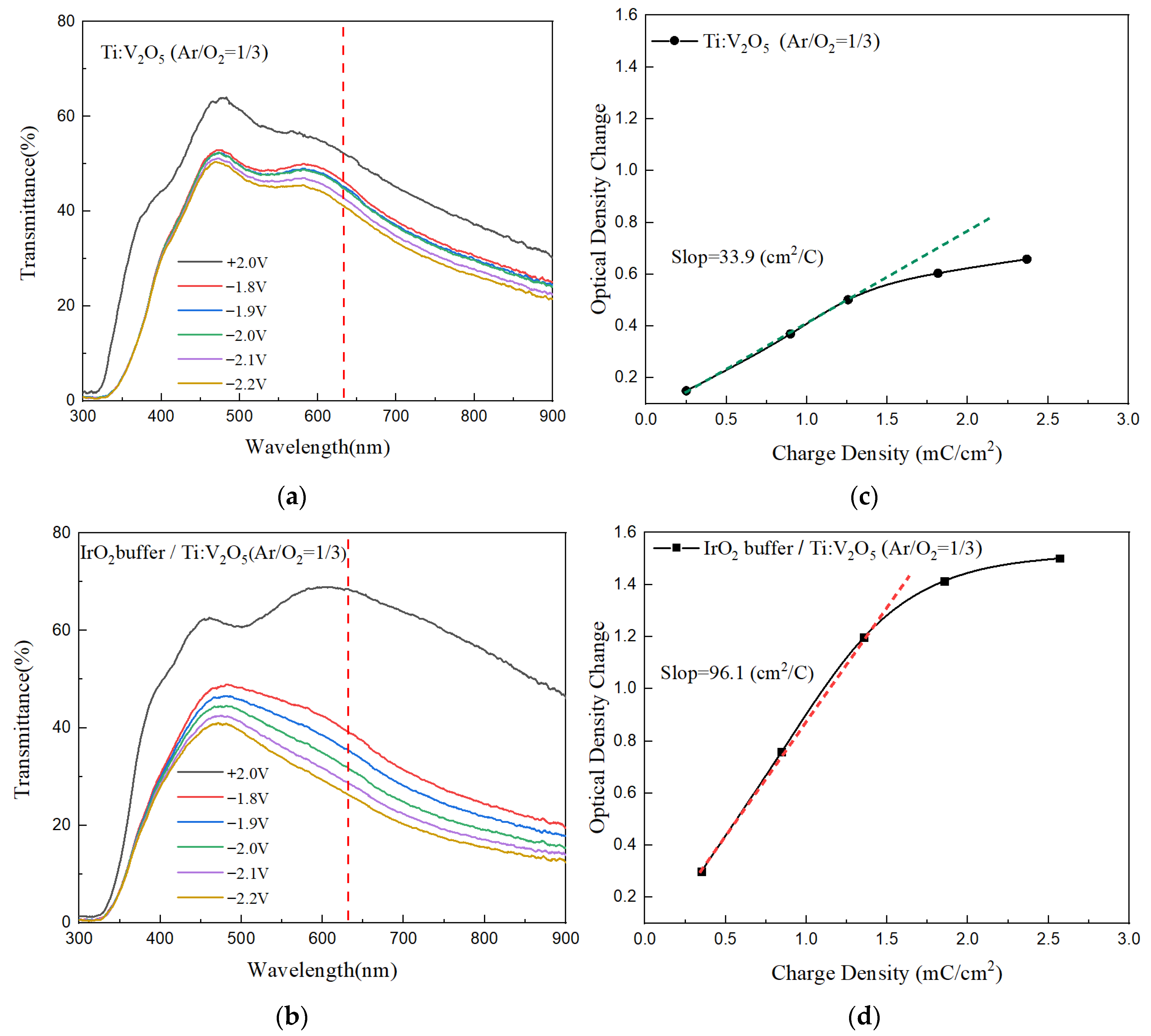
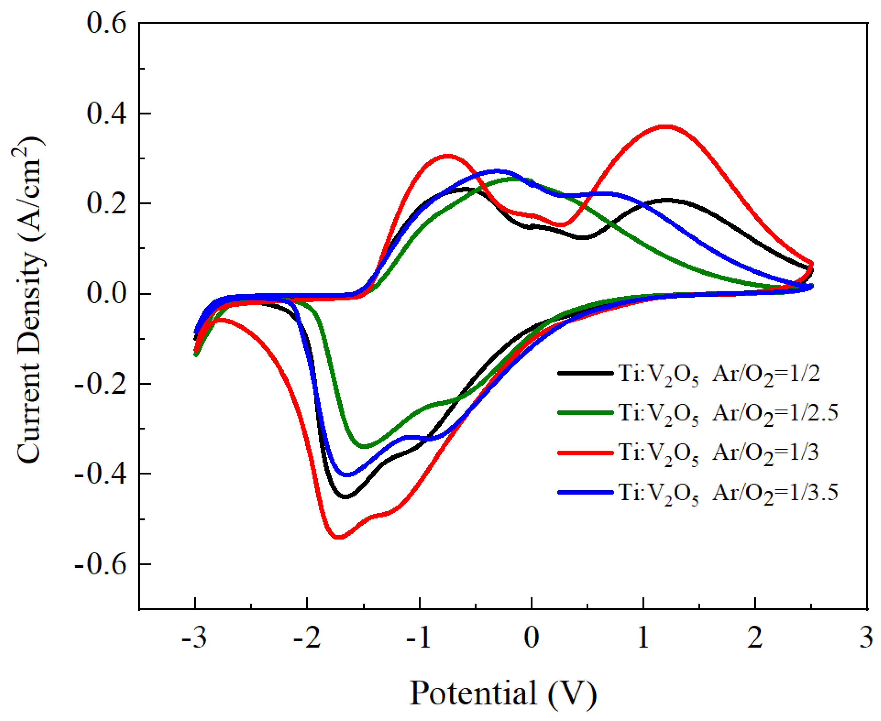
3.1. Ti:V2O5/ITO Films: Electrochemical and Optical Properties

Cyclic voltammetry (CV) was implemented to acquire the electrochemical properties of the Ti:V2O5 counter electrode on ITO glass. Figure 3 demonstrates the plot of current density versus potential voltage at the 25th cycle with an applied sweep voltage ranging from −3 V (coloring) to 2.5 V rate (bleaching) and a scan rate of 100 mV/s. The Ti:V2O5 films were processed with various Ar/O2 gas flow ratios (1/2, 1/2.5, 1/3, and 1/3.5) on ITO glass. However, the Ar/O2 gas flow ratio of 1/3 resulted a larger enveloped area, indicating that more Li+ ions participated in the electrochemical redox reaction [39]. In addition, the CV curve of the Ti:V2O5 films presents two remarkable cathodic reduction peaks (−1.2 V, −1.7 V) and two anodic peaks (−0.75 V, 1.5 V), which were attributed to Li+ intercalaltion and Li+ extraction, respectively. This higher optical transmittance modulation is a result of the larger CV envelope area on account of the increased number of Li ions into/out of the electrode interface.
Figure 4 demonstrates the coloring/bleaching in situ optical transmittance of the Ti:V2O5 electrode films at a wavelength of 633 nm, when applying the same voltage range (−3 V to 2.5 V) with various Ar/O2 gas flow ratios.
Figure 5 contrasts the coloring/bleaching transmittance modulation. An Ar/O2 gas flow ratio of 1/3 of Ti:V2O5 resulted in the highest optical transmittance of ∆T = 27% (from Tbleaching (57%) to Tcoloring (30%)). This result is in accordance with the cyclic voltammetry (CV) of the 1/3 ratio in Figure 3 and in our previous work [38]. This behavior could be explained by the larger enveloped area and large optical modulation achieved during CV. Electrochromism of the film upon Li+ intercalation/extraction was examined by transmittance measurement during the CV process. Considering the highest transmittance (∆T = 27%), we picked an Ar/O2 gas flow ratio of 1/3 as the best condition for buffer deposition on the ECD counter electrode.

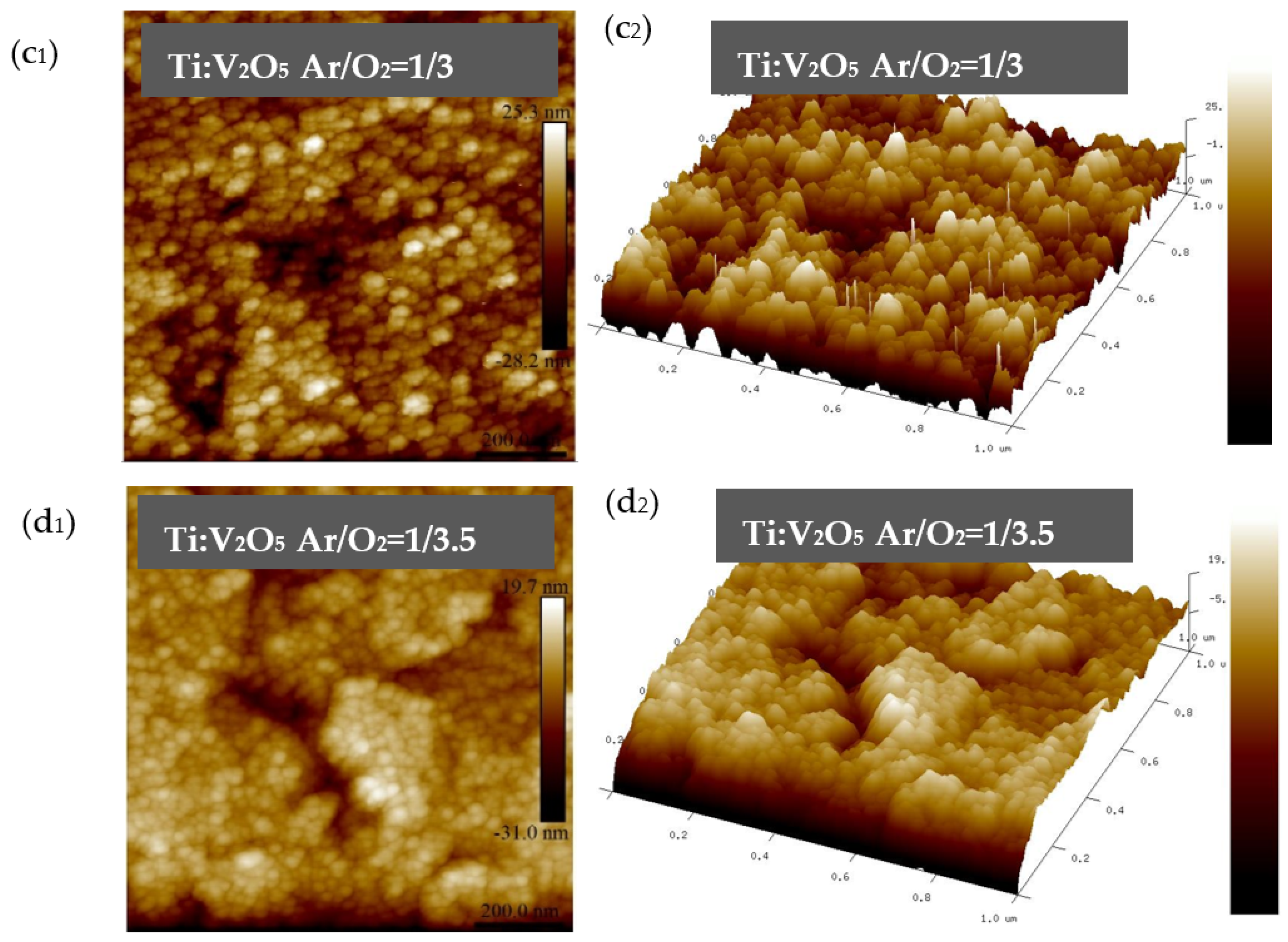
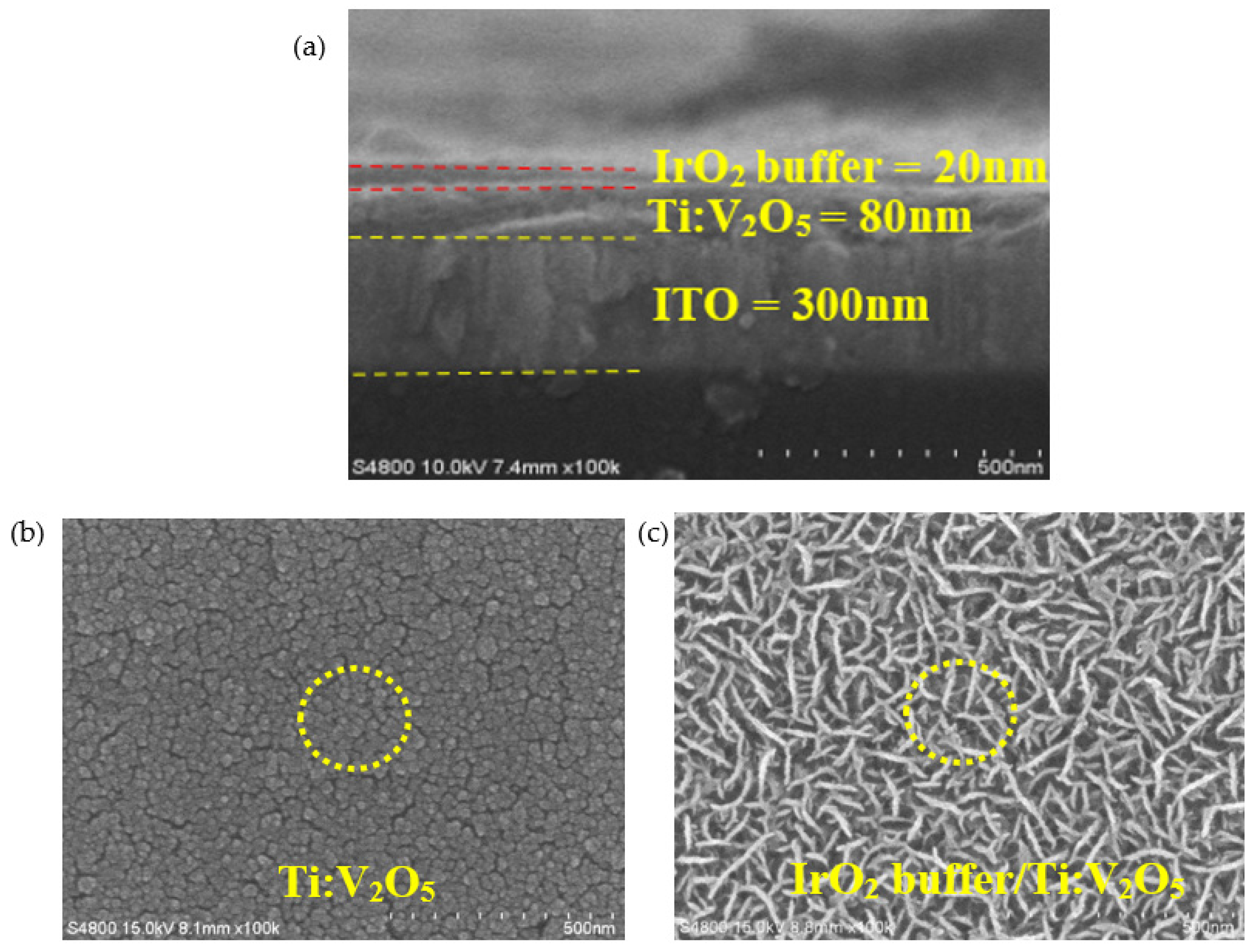
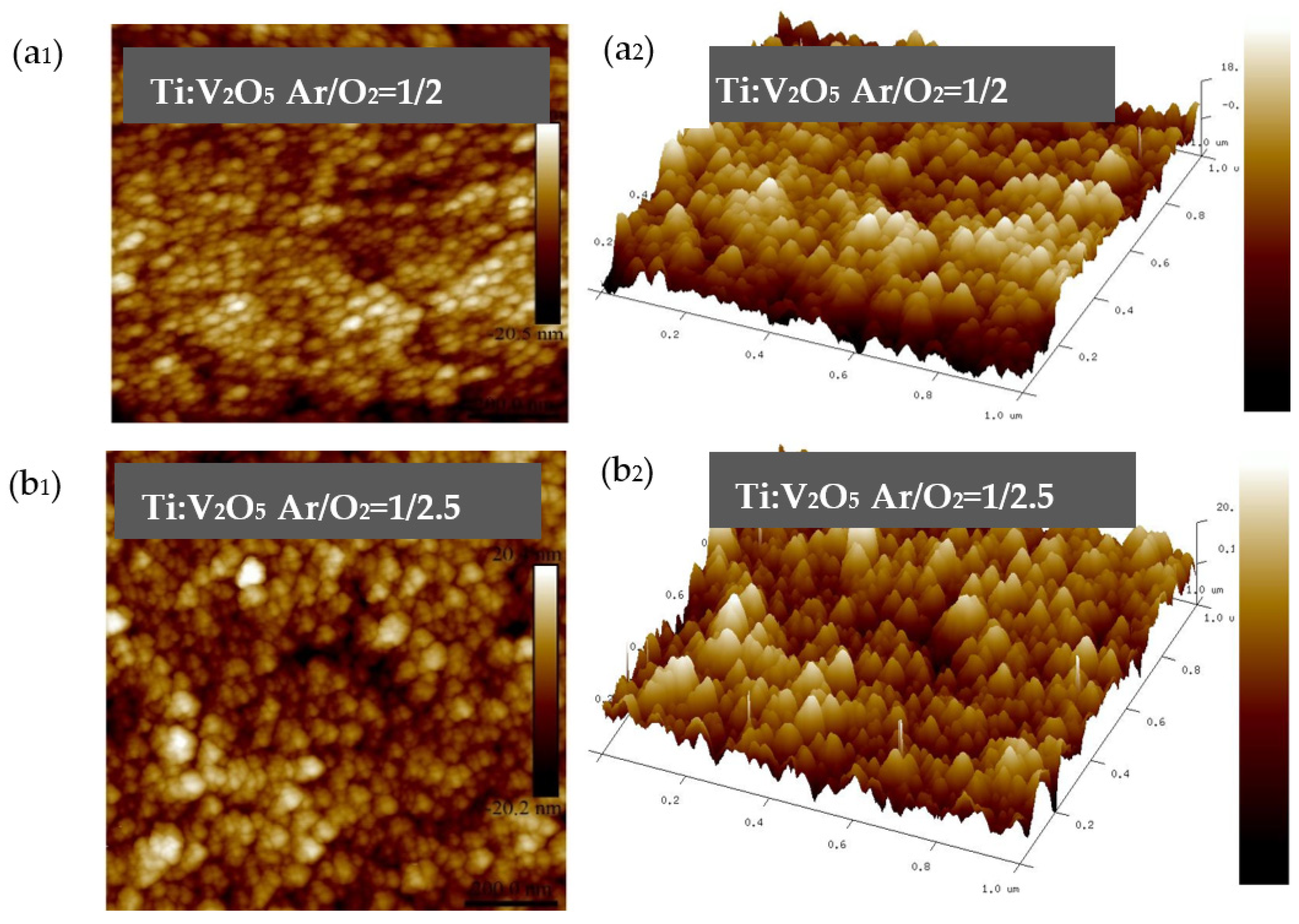
3.2. Ti:V2O5/ITO Films: Surface Roughness Properties

To understand the interfacial structure, the surface roughness of Ti:V2O5 counter electrodes on ITO glass was collected by AFM to investigate the film surface topography deposited with different Ar/O2 gas flow ratios (samples 1–4). Figure 5 shows the Ti:V2O5 film visualization of AFM in two dimensions (2D) and three dimensions (3D). In order to present the images, a scan area of 1 × 1 µm2 was used. The measurements of topographical parameters are listed in Table 3.
This work focuses on fabricating Ti:V2O5 films as a counter electrochromic layer by CAP deposition through four different oxygen and argon ratios. Here, we focus on how to fabricate nanostructure and surface roughness, so as to enhance fast ion insertion/extraction. According to the Thornton model [7,40], a loose-packed porous structure is formed under high-pressure environments. Arc discharge can be operated in high working pressure environments; interesting phenomena may occur such as self-organized synthesis of nanostructure and reduction in macroparticle size. When the arc is operated at higher working pressures, intense ion bombardment and ohmic heating likely allow a switch to thermionic mode; in this case, the erosion craters become smaller, facilitating the formation of a columnar structure. Figure 6 shows that Ar/O2 gas flow ratio of 1/3 led to the smallest average roughness (Ra) 3.9 nm and the Ti:V2O5 film surface was peak-shaped. In contrast with other ratios, the higher (1/3.5) or lower (1/2 and 1/2.5) Ar/O2 gas flow ratios led to a higher average roughness (Ra). This result indicated that the smallest Ra was consistent with the cyclic voltammetry (CV) results for the Ar/O2 gas flow ratio of 1/3 (sample 3), due to it having a larger enveloped area, which enables the particles to gain energy to migrate along the surface. The enveloped area of the CV curve correlated with the film surface topography. Under the electrochemical redox reaction of the Ti:V2O5 film, the topography may have the crucial influence on the insertion/extraction of Li ions at the counter electrode.
The surface roughness of the electrode is an essential indicator for light scattering. As shown in Figure 6, the gas flow ratio of 1/3 for Ti:V2O5 resulted in the highest optical transmittance (∆T = 27%), based on the smallest average roughness (Ra). The higher transmittance obtained might be ascribed to the reduction in light scattering [40]. The counter electrode surface deposited on the smallest Ra value could provide a prominent platform to insert the IrO2 buffer layer for fabricating an ideal ECD.

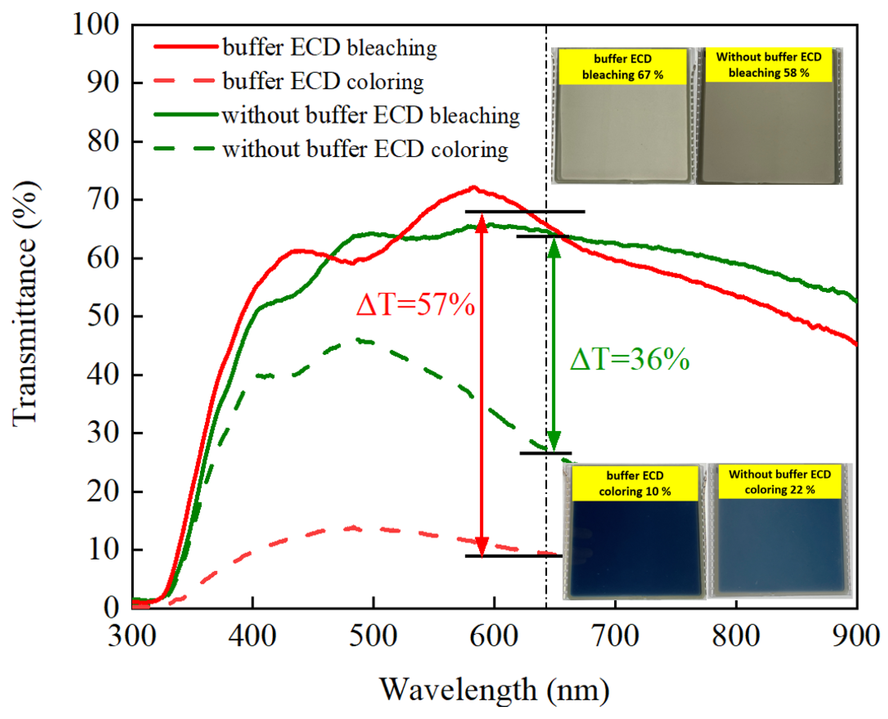
3.3. IrO2 Buffer/Ti:V2O5/ITO Films: Coloration Efficiency Analysis

Coloration efficiency (CE) is an imperative criterion for evaluating the assessment of electrochemical performance. It is defined as the change in optical density (ΔOD) per unit insert charge Qin (Qin = Q/A, which is the charge (Q) per unit area (A) of the electrode film). The calculation can be formulated as follows:
CE = ΔOD/Qin
ΔOD = ln (Tbleaching/Tcoloring)
where Tbleaching and Tcoloring are the transmittance values of the bleaching and coloring states at the specific wavelength of 633 nm, respectively.
The optical transmittance spectra and CE value of Ti:V2O5 film and IrO2 buffer/Ti:V2O5/ITO film were determined for the gas flow ratio of 1/3 (sample 3).The amount of charge intercalated (Qin) when a negative potential is applied were was integrated by chronoamperometry (CA) measurement. A high CE value (cm2C−1) is achieved when a large change in optical density is driven by a low amount of inserted charge. In Figure 7a,b, the optical transmittance spectra of Ti:V2O5 film and IrO2 buffer/Ti:V2O5 film with gradually applied successive potential voltages from +2.0 V (bleaching state) to −2.2 V (coloring state) during a pulsed time interval of 90 s are shown. The change in optical transmittance corresponds to the voltage between the lowest transmittance in the coloring state (Tcoloring) and the highest transmittance in the bleaching state (Tbleaching). The two electrode films were subjected to gradually decreasing voltages in accordance with the decreasing transmittance. The ΔOD value was nearly linear. The coloring/bleaching states were determined by the positive/negative voltage. IrO2 buffer/Ti:V2O5 film demonstrated lower transmittance than the Ti:V2O5 film at the coloring state due to inserting a buffer.
Figure 7c,d shows the optical density change vs. charge density of Ti:V2O5 films and IrO2 buffer/Ti:V2O5 films. The higher CE values indicate that electrodes can provide large optical modulation with small quantities of Li+ intercalation/extraction [40,41]. The CE value is calculated from the slope of the line fitted to the linear region of the curve. Compared with the two curves, the CE value of the IrO2/Ti:V2O5 film (96.1 cm2/C) is significantly higher than that of the Ti:V2O5 film (33.1 cm2/C). The Ti:V2O5 film with an IrO2 buffer layer provided a higher CE value and is good for promoting optical transmittance.

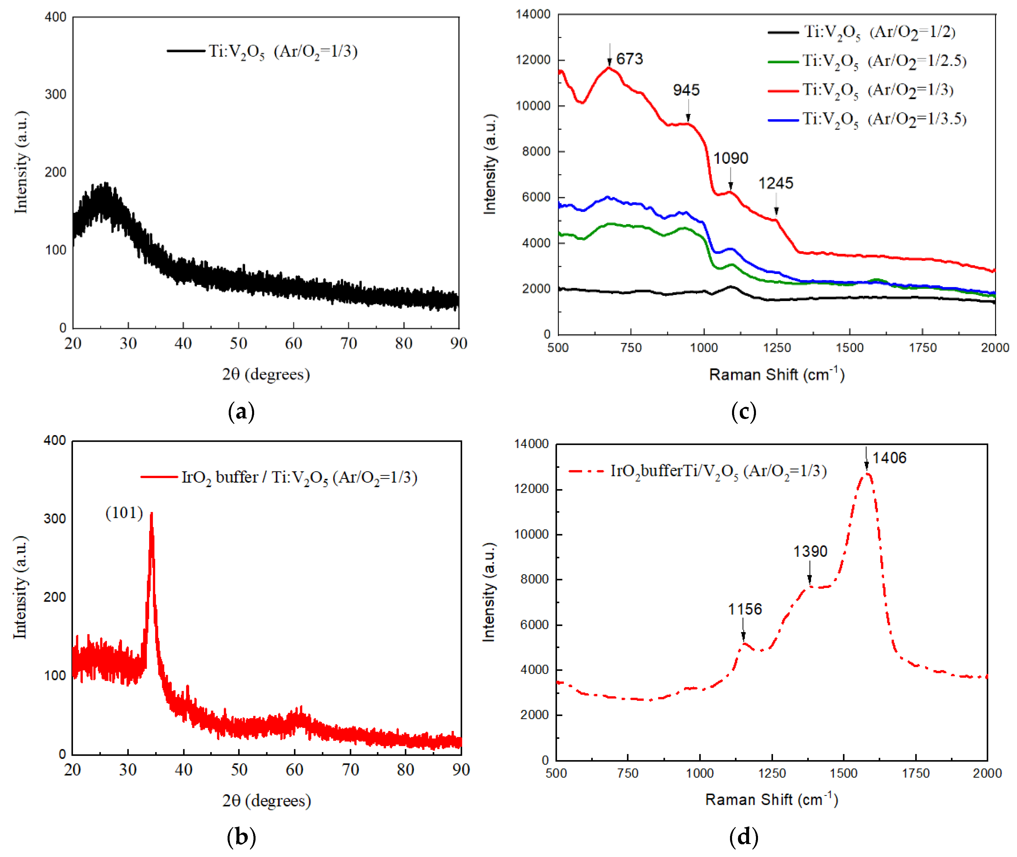
3.4. IrO2 Buffer/Ti:V2O5/ITO Films: X-ray Diffraction and Raman Spectroscopy

Figure 8a,b shows X-ray diffraction (XRD) of Ti:V2O5 films and IrO2 buffer/Ti:V2O5 film at an Ar/O2 ratio of 1/3. X-ray diffraction was used to assess the crystalline structure and phase in the scanning range from 20° to 90°. To determine the standard pattern identification, use was made of the Joint Committee on Powder Diffraction Standard (JCDPS).
Figure 8a shows that the XRD spectrum of Ti:V2O5 films (Ar/O2 ratio of 1/3) lacked the main peak, which indicates that the film could be an amorphous structure. The characteristics of the Ti:V2O5 films were not found in the XRD pattern.
Figure 8b shows the XRD spectrum of the IrO2 buffer/Ti:V2O5 film. The most intense diffraction peak was located at a 2θ angle of 34° (JCPDS card no. 47-1049) and corresponded to a preferential orientation of (101), which stacked along the c-axis. As our report investigates the influence of inserting the buffer, it can be observed that the use of IrO2 as a buffer on the Ti:V2O5 film (Ar/O2 ratio of 1/3) is an effective way to improve the crystallinity. As shown in Figure 8b, the IrO2 buffer/Ti:V2O5 film can obtain higher optical transmittance ∆T (from Tbleaching to Tcoloring) than the Ti:V2O5 film (Figure 8a). The crystallinity characteristic of the counter electrode films is closely associated with their transmittance.
The vibrations measured in Raman spectroscopy are determined by material structure shown in Figure 8c. Raman spectra of the Ti:V2O5 films produced by various Ar/O2 gas flow ratios (1/2, 1/2.5, 1/3 and 1/3.5) in the wavelength range of 500 cm−1 to 2000 cm−1 are shown. We found that, with an Ar/O2 gas flow ratio of 1/3, the Ti:V2O5 film exhibits a clearer and more intense band at 673 cm−1 and broader bands at 945 cm−1, 1090 cm−1, and 1245 cm−1 compared to other ratios, which have uncharacteristic Raman spectra. However, in comparison with Figure 8d, the IrO2 buffer/Ti:V2O5 film (Ar/O2 gas flow ratio of 1/3) has a distinguishable sharp band at 1406 cm−1 and broad bands at 1390 cm−1 and 1156 cm−1, corresponding to the crystalline preferential orientation of (101) in Figure 8b. After inserting the buffer in the Ti:V2O5 films (Ar/O2 gas flow ratio of 1/3), these bands disappeared.

3.5. IrO2 Buffer/Ti:V2O5/ITO Films: Surface Morphology

Figure 9a shows the cross-section morphology of the IrO2 buffer/Ti:V2O5 film at an Ar/O2 gas flow ratio of 1/3. The 100 nm electrode thickness includes IrO2 buffer of 20 nm and Ti:V2O5 film of 80 nm. The IrO2 buffer/Ti:V2O5 is stacked on indium tin oxide (ITO) glass substrate with a thickness of 300 nm. Figure 9b,c compares the surface morphology of the two materials. Figure 9b shows a Ti:V2O5/ITO film at an Ar/O2 gas flow ratio of 1/3. This is a featureless structure with a smooth and uneven, flakey surface. It might be related to the amorphous structure in Figure 8a imaged by XRD spectroscopy.
In Figure 9c, the IrO2 buffer on the Ti:V2O5 film at an Ar/O2 ratio of 1/3 is shown. It has a filamentary and interconnected structure. The morphological result is identical to our previous research [38]. As we found previously, this type of structure is useful for the transfer of Li ions in/out of the interface of the electrode due to the morphology, which possesses a larger inner pore that furnishes a great contact area and abundant porosity. This also proved that the filamentary and interconnected type of structure exhibits higher optical transmittance in Figure 7b and CE value (96.1 cm2/C) in Figure 7d of the IrO2 buffer/Ti:V2O5 film than optical transmittance in Figure 7a and CE value (33.9 cm2/C) in Figure 7b of the Ti:V2O5 film.

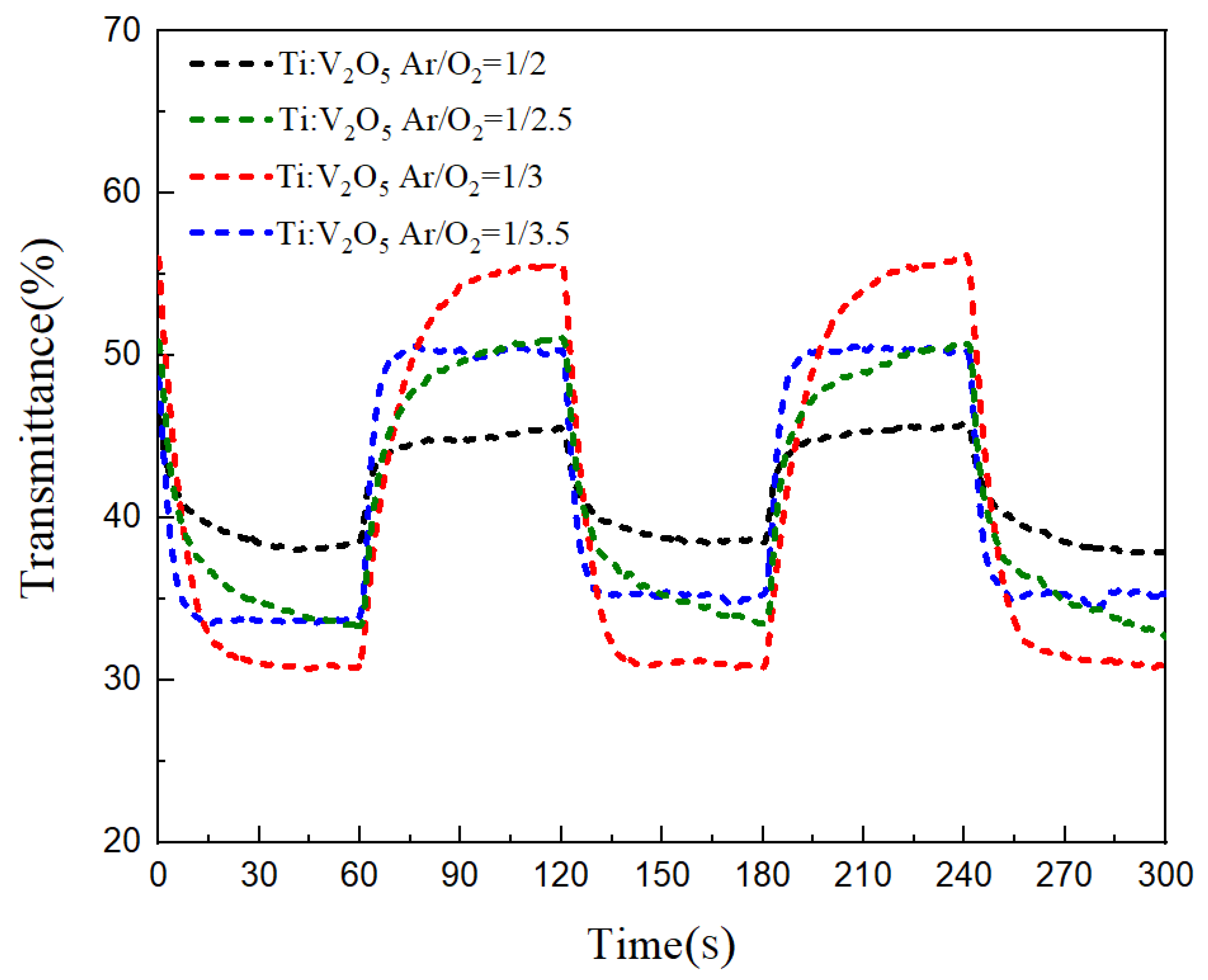
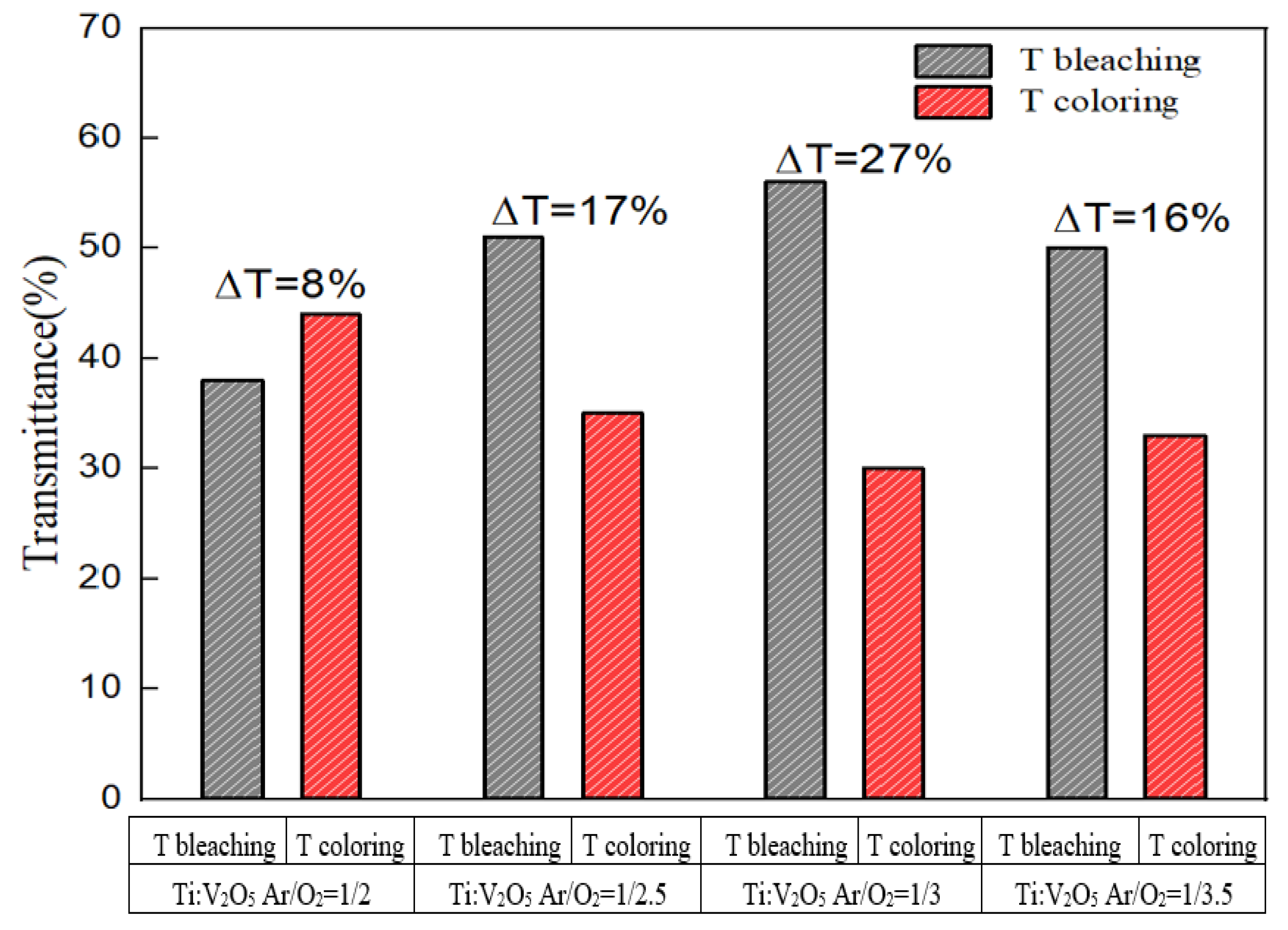
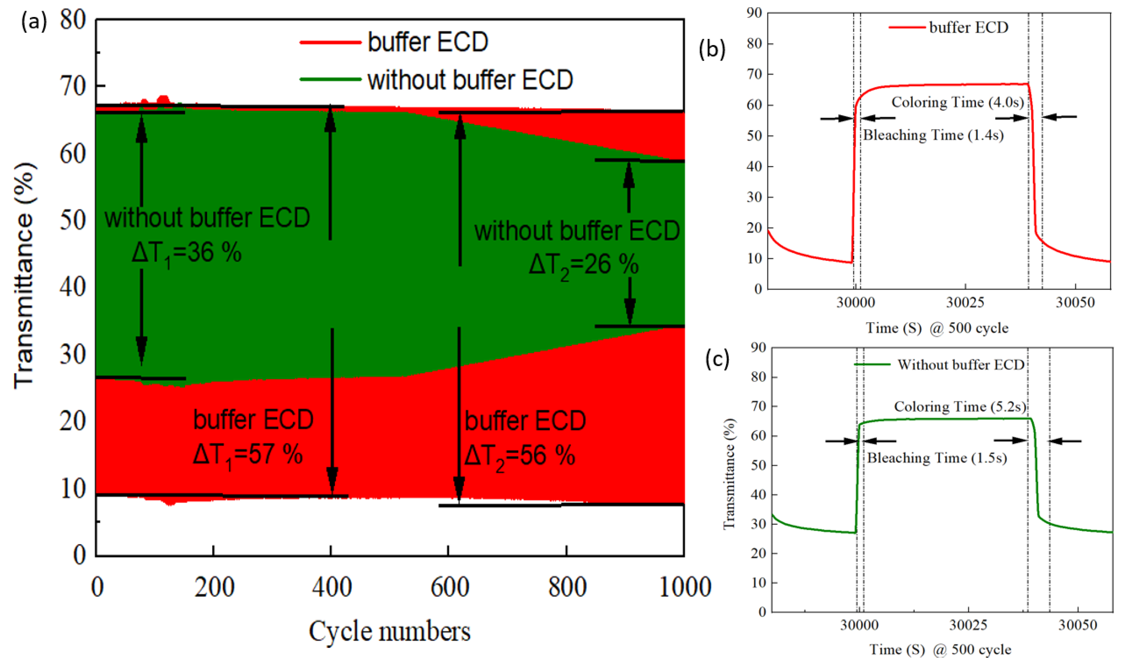
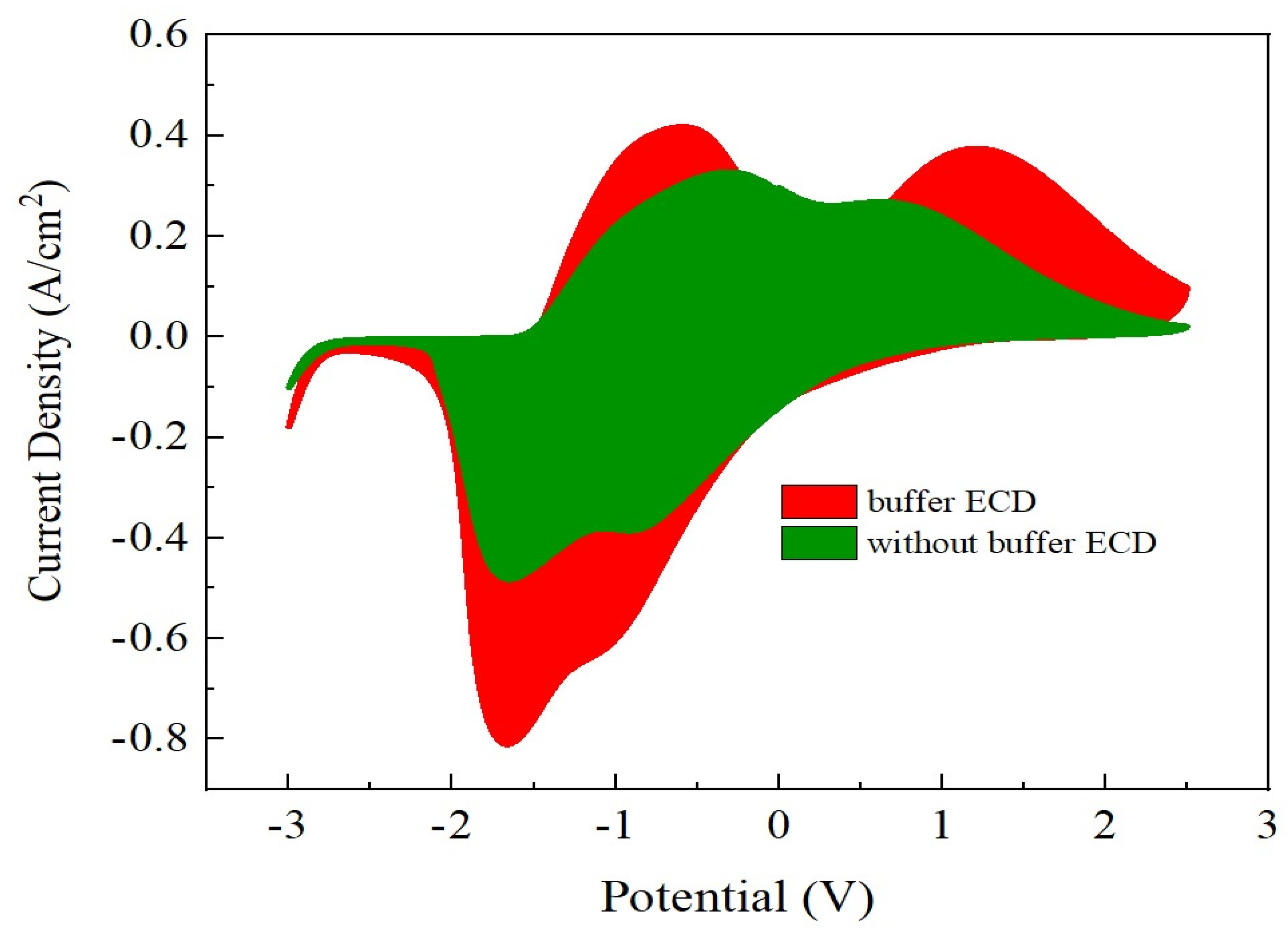
3.6. Buffer ECD: Optical Transmittance and Durability

Figure 10 demonstrates the optical transmittance spectra comparison with buffered ECD and without buffered ECD at bleaching/coloring state, based on the continuous potential voltage 2.5 V to −3 V. For the buffered ECD (glass/ITO/WO3/liquid electrolyte/IrO2 buffer/Ti:V2O5(Ar/O2 ratio 1/3)/ITO/glass), the optical transmittance modulation was ∆T = 57% (from Tbleaching (67%) to Tcoloring (10%)) at 633 nm, in the range from 300 nm to 1000 nm, which was higher than without the buffer (ITO/WO3/liquid electrolyte/Ti:V2O5 (Ar/O2 ratio 1/3)/ITO) (∆T = 36% (from Tbleaching (58%) to Tcoloring (22%)). This could be attributed to a larger CV enveloped area for the buffered-ECD, as shown in Figure 11, on account of the film with greater Li+ intercalation/extraction as shown by optical transmittance during the CV analysis. Remarkably, this result was in good agreement with Figure 3, in which the largest CV enveloped area demonstrated the highest transmittance.
The durability of the ECD is an important factor to determine whether the product can work in real life. Figure 12a presents the long-life (1000 cycles) durability comparison between the buffered ECD and the ECD without buffer. After 1000 cycles of bleaching/coloring, the buffered ECD had notable durability, retaining 98% (i.e., 2% decay) of the initial value, greater than 78% (22% decay) for the ECD without buffer. The high-contrast optical performance and good durability of the ECD could be attributed to the inserted IrO2 buffer on the electrode. We found that both optical transmittance and durability were, in terms of electrode surface morphology, equipped with filamentary and interconnect type structure. The buffer ECD with the IrO2 buffer/Ti:V2O5 electrode provided a higher CE value (96.1 cm2/C) to support the Li+ intercalation/extraction process. Figure 12b,c illustrates the buffered ECD and the ECD without buffer; after insertion of the buffer, the switching response time was from 1.4 s in the bleaching state to 4.0 s in the coloring state, which was faster than the ECD without buffer (response time was from 1.5 s in the bleaching state to 5.2 s in the coloring state). In addition, we also survey the comparison of recent research on electrodes under various conditions in Table 4.

4. Conclusions

We established an appropriate electrode, Ti:V2O5, as a base to insert a buffer. According to our results, the buffer inserted on the Ti:V2O5 electrode film with exclusive surface morphology not only effectively increased the coloration efficiency (CE), but also promoted optical transmittance and durability. Moreover, strategies such as Ti:V2O5 films are based on a series of Ar/O2 gas flow ratios (1/2, 1/2.5, 1/3, and 1/3.5) on indium tin oxide (ITO) glass to establish the appropriate electrode.
Subsequently, we picked the Ti:V2O5 film with an Ar/O2 gas flow ratio of 1/3 as the best electrode base. This film had the largest cyclic voltammetry (CV) area to allow more Li ions into/out of the electrode interface and presented the highest optical transmittance (∆T) of 27%. Atomic force microscopy (AFM) was performed to obtain a deep understanding of the surface topography of the electrode interface. In addition, this value of Ti:V2O5 (Ar/O2 = 1/3) is helpful for optical transmittance, as it possesses the smallest average roughness (Ra = 3.53 nm) to reduce light scattering.
To distinguish the difference when the buffer was inserted on the electrode, we implemented many analyses. Regarding coloration efficiency (CE), the IrO2 buffer/Ti:V2O5 film achieved a higher value (96.1 cm2/C), providing large optical modulation, than the Ti:V2O5 film without buffer (33.9 cm2/C). Regarding crystallinity, the IrO2 buffer/Ti:V2O5 film, which has an intense diffraction peak at a 2θ angle of 34° and a preferential orientation of (101), is better than the Ti:V2O5 film, which has an amorphous structure. Regarding surface morphology, the IrO2 buffer/Ti:V2O5 film with a filamentary and interconnected structure, which provides larger inner pore and contact area, improves Li ion transfer in/out interface of the electrode compared with the Ti:V2O5 film with a featureless structure.
We successfully fabricated a buffered ECD via a vacuum cathodic arc plasma (CAP) technique. Our goal was to insert the IrO2 buffer to enhance the properties of the ECDs. Compared to the ECD without buffer, the buffered ECD promoted optical transmittance modulation (∆T = 57%) and maintained excellent durability of up to 98% (2% decay). This may provide a new insight into the development of energy devices. The superior electrochromic performance with the buffer layer makes our ECD a prominent candidate for use in smart windows with reduced energy demand.

Author Contributions

The study was written and writed–original draft by T.-F.K. and reviewed by P.-W.C., The data collection and analysis for ECD were conducted by T.-F.K., P.-W.C. and H.-T.Y.; The manuscripts were prepared by K.-M.L. and H.-T.Y. All authors have read and agreed to the published version of the manuscript.

Funding

This research was funded by Division of Physics, Institute of Nuclear Energy Research (INER), Taiwan and National Taiwan University under the Excellence Improvement Program for Doctoral Students (grant number 108-2926-I-002-002-MY4), sponsored by Ministry of Science and Technology, Taiwan.

Institutional Review Board Statement

Not applicable.

Informed Consent Statement

Not applicable.

Data Availability Statement

The data presented in this study are available on request from the corresponding author. The data are not publicly available due to privacy.

Conflicts of Interest

The authors declare no conflict of interest.

References

  1. Granqvist, C.G. Electrochromics for smart windows: Oxide-based thin films and devices. Thin Solid Films 2014, 564, 1–38. [Google Scholar] [CrossRef]
  2. Chang, J.Y.; Chen, Y.C.; Wang, C.M.; Wang, W.N.; Wen, C.Y.; Lin, J.M. Electrochromic properties of Lithium-doped tungsten oxide prepared by electron beam evaporation. Coatings 2019, 9, 191. [Google Scholar] [CrossRef] [Green Version]
  3. Kim, K.H.; Koo, B.R.; Ahn, H.J. Title of the chapter Sheet resistance dependence of fluorine-doped tin oxide films for high-performance electrochromic devices. Ceram. Int. 2018, 44, 9408–9413. [Google Scholar] [CrossRef]
  4. Jiang, B.; Lou, B.; Li, J.; Peng, P.; Chen, J.W.; Chu, L.H.; Li, Y.F.; Li, M.C. Electrochemical effect of graphite fluoride modification on Li-rich cathode material in lithium ion battery. Ceram. Int. 2019, 45, 160–167. [Google Scholar] [CrossRef]
  5. Runnerstrom, E.L.; Llorde’s, A.; Lounisac, S.D.; Milliron, D.J. Nanostructured electrochromic smart windows: Traditional materials and NIR-selective plasmonic nanocrystals. Chem. Commun. 2014, 50, 10555–10572. [Google Scholar] [CrossRef] [Green Version]
  6. Li, H.; McRaea, L.; Firby, C.J.; Hussein, M.A.; Elezzabi, A.Y. Nanohybridization of molybdenum oxide with tungsten molybdenum oxide nanowires for solution-processed fully reversible switching of energy storing smart windows. Nano Energy 2020, 47, 130–139. [Google Scholar] [CrossRef]
  7. Chen, P.W.; Chang, C.T.; Ko, T.F.; Hsu, S.C.; Li, K.F.; Wu, J.Y. Fast response of complementary electrochromic device based on WO3/NiO electrodes. Sci. Rep. 2020, 10, 8430. [Google Scholar] [CrossRef]
  8. Issam, M.; Gaudon, M.; Song, G.; Labrugere, C.; Rougier, A. Crystallized V2O5 as oxidized phase for unexpected multicolor electrochromism in V2O3 thick film. ACS Appl. Energy Mater. 2018, 1, 2721–2729. [Google Scholar]
  9. Niklasson, G.A.; Granqvist, C.G. Sol-gel fabrication of NiO and NiO/WO3 based electrochromic device on ITO and flexible substrate. Ceram. Int. 2020, 46, 8631–8639. [Google Scholar]
  10. Tritschler, U.; Beck, F.; Schlaad, H.; Cölfen, H. Electrochromic properties of self-organized multifunctional V2O5 polymer hybrid films. J. Mater. Chem. C 2015, 3, 950–954. [Google Scholar] [CrossRef] [Green Version]
  11. Salek, G.; Bellanger, B.; Mjejri, I.; Gaudon, M.; Rougier, A. Polyol Synthesis of Ti-V2O5 Nanoparticles and Their Use as Electrochromic Films. Inorg. Chem. 2016, 55, 9838–9847. [Google Scholar] [CrossRef]
  12. Xia, X.H.; Tu, J.P.; Zhang, J.; Wang, X.L.; Zhang, W.K.; Huang, H. Electrochromic properties of porous NiO thin flms prepared by a chemical bath deposition. Sol. Energy Mater. Sol. Cells 2008, 92, 628–633. [Google Scholar] [CrossRef]
  13. Subrahmanyam, A.; Kumar, C.S.; Karuppasamy, K.M. A note on fast protonic solid state electrochromic device: NiOx/Ta2O5/WO3−x. Sol. Energy Mater. Sol. Cells 2007, 91, 62–66. [Google Scholar] [CrossRef]
  14. McRae, L.; Li, H.; Elezzabi, A.Y. Solution-processed interfacial PEDOT: PSS assembly into porous tungsten molybdenum oxide nanocomposite flms for electrochromic applications. ACS Appl. Mater. Interfaces 2018, 10, 10520–10527. [Google Scholar]
  15. Lang, F.; Liu, J.; Wang, H.; Yan, H. NiO nanocrystalline/reduced graphene oxide composite film with enhanced electrochromic properties. Nano 2017, 12, 1750058. [Google Scholar] [CrossRef]
  16. Cai, G.; Darmawan, P.; Cui, M.; Chen, J.; Wang, X.; Eh, A.L.S.; Magdassi, S.; Lee, P.S. Inkjet-printed all solid-state electrochromic devices based on NiO/WO3. Nanoscale 2016, 8, 348–357. [Google Scholar] [CrossRef]
  17. Chang, C.C.; Chi, P.W.; Chandan, P.; Lin, C.K. Electrochemistry and Rapid ElectrochromismControl of MoO3/V2O5 Hybrid Nano bilayers. Nat. Mater. 2019, 12, 2475. [Google Scholar] [CrossRef] [Green Version]
  18. Mouratis, K.; Tudose, V.; Romanitan, C.; Pachiu, C.; Tutunaru, O.; Suchea, M.; Couris, S.; Vernardou, D.; Emmanouel, K. Electrochromic Performance of V2O5 Thin Films Grown by Spray Pyrolysis. Materials 2020, 13, 3859. [Google Scholar] [CrossRef]
  19. Wei, Y.; Zhou, J.; Xu, C. Improved stability of electrochromic devices using Ti-doped V2O5 film. Electrochim. Acta 2015, 166, 277–284. [Google Scholar] [CrossRef]
  20. Zeng, H.; Liu, D.; Zhang, Y.; See, K.A.; Jun, Y.S.; Wu, G.; Gerbec, J.A.; Ji, X.; Stucky, G.D. Nanostructured Mn-Doped V2O5 Cathode Material Fabricated from Layered Vanadium Jarosite. Chem. Mater. 2015, 27, 7331–7336. [Google Scholar] [CrossRef] [Green Version]
  21. Vernardou, D.; Marathianou, I.; Katsarakis, N.; Koudoumas, E.; Kazadojev, I.I.; O’Brien, S.; Pemble, M.E.; Povey, I.M. Capacitive behavior of Ag doped V2O5 grown by aerosol assisted chemical vapour deposition. Electrochim. Acta 2016, 196, 294–299. [Google Scholar] [CrossRef]
  22. Venkatesan, A.; Chandar, N.R.K.; Pradeeswari, K.; Pandi, P.; Kandasamy, A.; Kumar, R.M.; Jayavel, R. Influence of Al doping on structural, luminescence and electrochemical properties of V2O5 nanostructures synthesized via non-hydrolytic sol-gel technique. Mater. Res. Express 2019, 6, 015017. [Google Scholar] [CrossRef]
  23. Anil, K.; Sahay, P.P. Influence of Ti doping on the microstructural and electrochromic properties of dip-coated nanocrystalline V2O5 thin films. J. Solgel Sci. Technol. 2020, 95, 34–51. [Google Scholar]
  24. Tian, S.; Xing, A.; Tang, H.; Bao, Z.H.; Wu, G.M. Enhanced cycling stability of TiO2-coated V2O5 nanorods through a surface sol–gel process for lithium ion battery application. J. Mater. Chem. A 2014, 2, 2896. [Google Scholar] [CrossRef]
  25. Madhavi, V.; Kumar, P.J.; Kondaiah, P.; Hussain, O.M.; Uthanna, S. Efect of molybdenum doping on the electrochromic properties of tungsten oxide thin fms by RF magnetron sputtering. Ionics 2014, 20, 1737–1745. [Google Scholar] [CrossRef]
  26. Pattarapon, P.; Son, Y.H.; Sung, Y.M.; Ok, J.W. The effect of sputtering Ar gas pressure on optical and electrical properties of flexible ECD device with WO3 electrode deposited by RF magnetron sputtering on ITO/PET substrate. Opt. Mater. 2022, 123, 111829. [Google Scholar]
  27. Panagopoulou, M.; Vernardou, D.; Koudoumas, E.; Tsoukalas, D.; Raptis, Y.S. Oxygen and temperature effects on the electrochemical and electrochromic properties of rf-sputtered V2O5 thin films. Electrochim. Acta 2017, 232, 54–63. [Google Scholar] [CrossRef]
  28. Liu, Y.; Jia, C.; Wan, Z.; Weng, X.; Xie, J.; Deng, L. Electrochemical and electrochromic properties of novel nanoporous NiO/V2O5 hybrid film. Sol. Energy Mater. Sol. Cells 2015, 132, 467–475. [Google Scholar] [CrossRef]
  29. Najdosk, M.; Koleva, V.; Samet, A. Effect of deposition conditions on the electrochromic properties of nanostructured thin films of ammonium intercalated vanadium pentoxide xerogel. J. Phys. Chem. C 2014, 118, 9636–9646. [Google Scholar] [CrossRef]
  30. Yu, D.M.; Zhang, S.T.; Liu, D.W.; Zhou, X.Y.; Xie, S.H.; Zhang, Q.F.; Liu, Y.Y.; Cao, G.Z. Effect of manganese doping on Li-ion intercalation properties of V2O5 films. J. Mater. Chem. 2010, 20, 10841–10846. [Google Scholar] [CrossRef]
  31. Loi, M.R.; Moura, E.A.; Westphal, T.M.; Balboni, R.D.C.; Gündelc, A.; Flores, W.H.; Pereira, M.B.; Santos, M.J.L.; Santos, J.F.L.; Pawlicka, A.; et al. Impact of Zr precursor on the electrochemical properties of V2O5 sol-gel films. J. Electroanal. Chem. 2019, 839, 67–74. [Google Scholar] [CrossRef]
  32. Moura, E.A.; Cholan, C.M.; Balboni, R.D.C.; Westphal, T.M.; Lemos, R.M.J.; Azevedo, C.F.; Gündel, A.; Flores, W.H.; Gomez, J.A.; Ely, F.; et al. Electrochemical properties of thin films of V2O5 doped with TiO2. J. Phys. Chem. Solids 2018, 119, 1–8. [Google Scholar] [CrossRef]
  33. Vasanth, R.D.; Ponpandian, N.; Mangalaraj; Viswanathan, C. Effect of annealing and electrochemical properties of sol–gel dip coated nanocrystalline V2O5 thin films. Mater. Sci. Semicond. Process. 2013, 16, 256–262. [Google Scholar] [CrossRef]
  34. Sinha, S.K. Effect of temperature on structural, optical and electrical properties of pulsed-laser deposited W-doped V2O5 thin films. Superlattices Microstruct. 2019, 25, 88–94. [Google Scholar] [CrossRef]
  35. Qiu, D.; Wu, J.; Liang, L.; Zhang, H.; Cao, H.; Yong, W.; Tian, T.; Gao, J.; Zhuge, F. Structural and electrochromic properties of undoped and Mo-doped V2O5 thin films by a two-electrode electrodeposition. J. Nanosci. Nanotechnol. 2018, 18, 7502–7507. [Google Scholar] [CrossRef]
  36. Wang, C.; Shi, Z.; Li, W.; Song, X.; Jia, S.; Wang, L. IEEE Transactions on Plasma Science. IEEE 2015, 43, 2267–2274. [Google Scholar]
  37. Thornton, J.A. Influence of apparatus geometry and deposition conditions on the structure and topography of thick sputtered coatings. J. Vac. Sci. Technol. 1974, 11, 666. [Google Scholar] [CrossRef]
  38. Ko, T.F.; Chen, P.W.; Li, K.M.; Young, H.T.; Chang, C.T.; Shu, S.C. High-Performance Complementary Electrochromic Device Based on Iridium Oxide as a Counter Electrode. Materials 2012, 14, 1591. [Google Scholar] [CrossRef]
  39. Liu, Q.; Chen, Q.; Zhang, Q.; Dong, G.; Zhong, X.; Xiao, Y.; Delplancke-Ogletree, M.P.; Reniers, F.; Diao, X. Dynamic behaviors of inorganic all-solid-state electrochromic device: Role of potential. Electrochim. Acta 2018, 269, 617–623. [Google Scholar] [CrossRef]
  40. Chen, P.W.; Chang, C.T.; Ali, M.; Wu, J.-Y.; Li, Y.-C.; Chen, M.-H.; Jan, D.-J.; Yuan, C.-T. Tantalum oxide film deposited by vacuum cathodic arc plasma with improved electrochromic performance. Sol. Energy Mater. Sol. Cells 2018, 182, 188–195. [Google Scholar] [CrossRef]
  41. Atak, G.; Coşkun, Ö.D. Annealing effects of NiO thin films for all-solid-state electrochromic devices. Solid State Ion. 2017, 305, 43–51. [Google Scholar] [CrossRef]
Figure 1. The schematic structure of buffered ECDs.
Materials 15 05179 g001
Figure 2. Illustration of cathodic arc plasma (CAP) technique.
Materials 15 05179 g002
Figure 3. CV curve of Ti:V2O5 electrode films with various Ar/O2 gas flow ratios at the 25th cycle with a scan rate of 100 mV/s.
Materials 15 05179 g003
Figure 4. In situ optical transmittance response at 633 nm of Ti:V2O5 electrode films with various Ar/O2 gas flow ratios.
Materials 15 05179 g004
Figure 5. The difference in coloring/bleaching transmittance modulation of Ti:V2O5 electrode films.
Materials 15 05179 g005
Figure 6. (a1d1) 2D AFM visualization of Ti:V2O5 film; (a2d2) 3D AFM visualization of Ti:V2O5 film.
Materials 15 05179 g006aMaterials 15 05179 g006b
Figure 7. (a,b) Optical transmittance spectra of Ti:V2O5 films and IrO2 buffer/Ti:V2O5 films at different applied potential voltages; (c,d) optical density change vs. charge density of Ti:V2O5 films and IrO2 buffer/Ti:V2O5 films.
Materials 15 05179 g007
Figure 8. (a,b) X-ray diffraction of Ti:V2O5 films and IrO2 buffer/Ti:V2O5 films at an Ar/O2 ratio of 1/3; (c,d) Raman spectroscopy of Ti:V2O5 films with various Ar/O2 ratios and IrO2 buffer/Ti:V2O5 at an Ar/O2 ratio of 1/3.
Materials 15 05179 g008
Figure 9. SEM images of surface morphology: (a) cross-section morphology of the IrO2 buffer/Ti:V2O5 film at Ar/O2 ratio 1/3; (b) Ti:V2O5 film at Ar/O2 ratio 1/3; (c) IrO2 buffer/Ti:V2O5 film at Ar/O2 gas flow ratio of 1/3.
Materials 15 05179 g009
Figure 10. The optical transmittance spectra and image comparison with buffered ECD and ECD without buffer in bleaching/coloring states.
Materials 15 05179 g010
Figure 11. The CV curve comparison between buffered ECD and ECD without buffer.
Materials 15 05179 g011
Figure 12. (a) The 1000-cycle durability comparison with buffered ECD and ECD without buffer, (b) buffered ECD and (c) ECD without buffer: switch response time @ 500 cycles.
Materials 15 05179 g012
Table 1. Deposition parameters of IrO2 buffer on Ti:V2O5 counter electrode films.
No.FilmAr/O2
(Ar = 20 sccm)
W.P.
(Torr)
DC Power
(W)
Deposition
Temp.
(°C)
Deposition
Time
(s)
Thickness
(nm)
Sample 1Ti:V2O51/22.1 × 10−312001008080
Sample 2Ti:V2O51/2.52.3 × 10−312001008080
Sample 3Ti:V2O51/32.5 × 10−312001008080
Sample 4Ti:V2O51/3.52.8 × 10−312001008080
Sample 5IrO2 buffer1/31.8 × 10−312501001020
Table 2. Deposition parameters of WO3 electrode film and ITO glass.
TargetAr/O2 (sccm)W.P.
(Torr)
DC
Power
(W)
Deposition
Time
(min)
Deposition Rate
(nm/min)
Deposition
Temp.
°C
Thickness
(nm)
W Metal1/3
(Ar = 100)
8 × 10−31500151350200
ITO1/3
(Ar = 100)
3 × 10−3500605200300
Table 3. Topographical parameters of Ti:V2O5 counter electrode films.
No.FilmAr/O2
Ratio
Image
Surface Area
(µm2)
Image Projected
Surface Area
(µm2)
Root Mean
Square Roughness
(nm)
Average
Roughness
(nm)
Sample 1Ti:V2O51/21.3317.225.63
Sample 2Ti:V2O51/2.51.2216.544.83
Sample 3Ti:V2O51/31.1015.013.91
Sample 4Ti:V2O51/3.51.2716.624.94
Table 4. Comparison of recent research on electrodes under various conditions.
Counter ElectrodeMethod∆T
(%)
CE
(cm2/C)
Switching Time
(tc/tb)
Ref.
IrO2 buffer/Ti:V2O5CAP5796.14.0/1.4 sThis work
IrO2CAP50-4.8/1.5 s[38]
V2O5polyol-mediated synthesis50--[8]
V2O5polymer
synthesis
338920/23 s[10]
Ti:V2O5polyol synthesis10--[11]
NiOspray pyrolysis37.4428/10 s[12]
V2O5spin coating31-8.2/6.3 s[17]
Publisher’s Note: MDPI stays neutral with regard to jurisdictional claims in published maps and institutional affiliations.

