
Effect of Sn Grain Orientation on Reliability Issues of Sn-Rich Solder Joints


Abstract
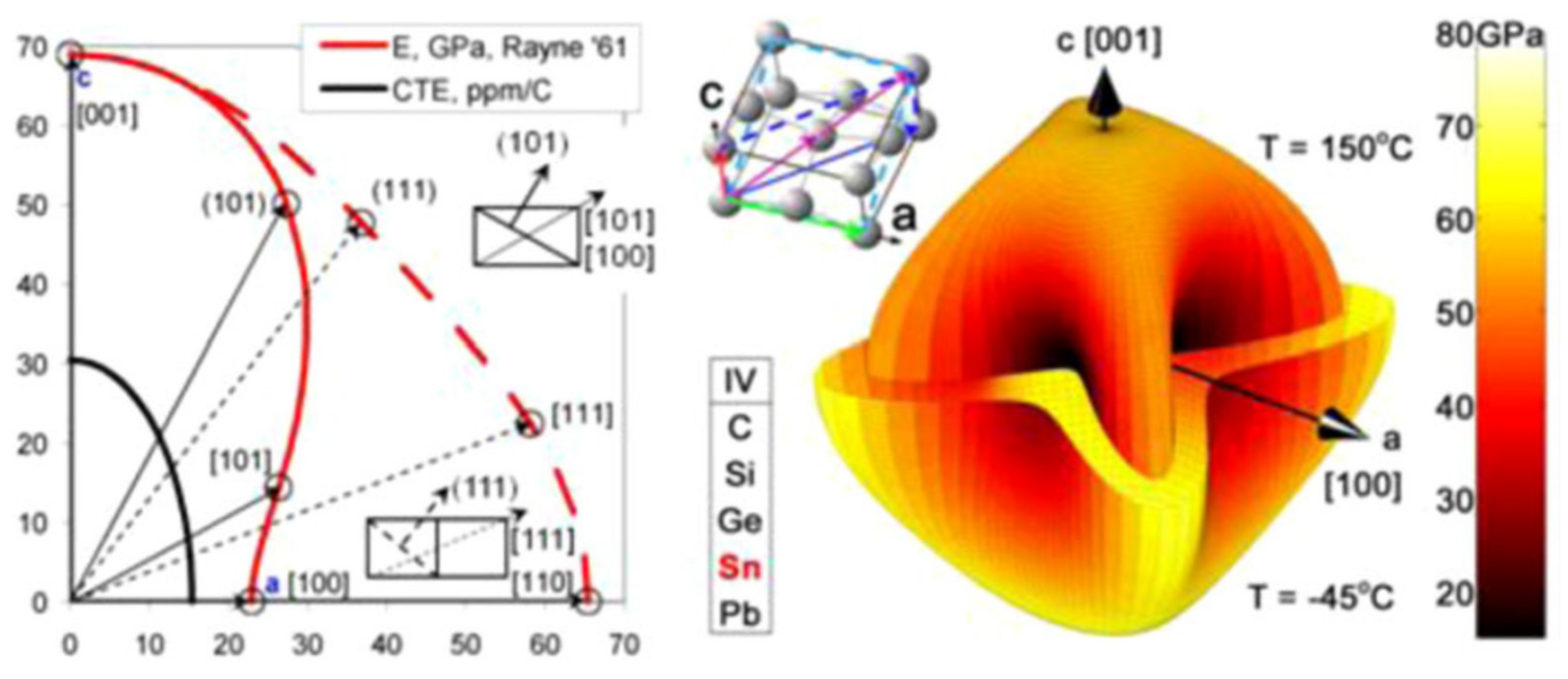
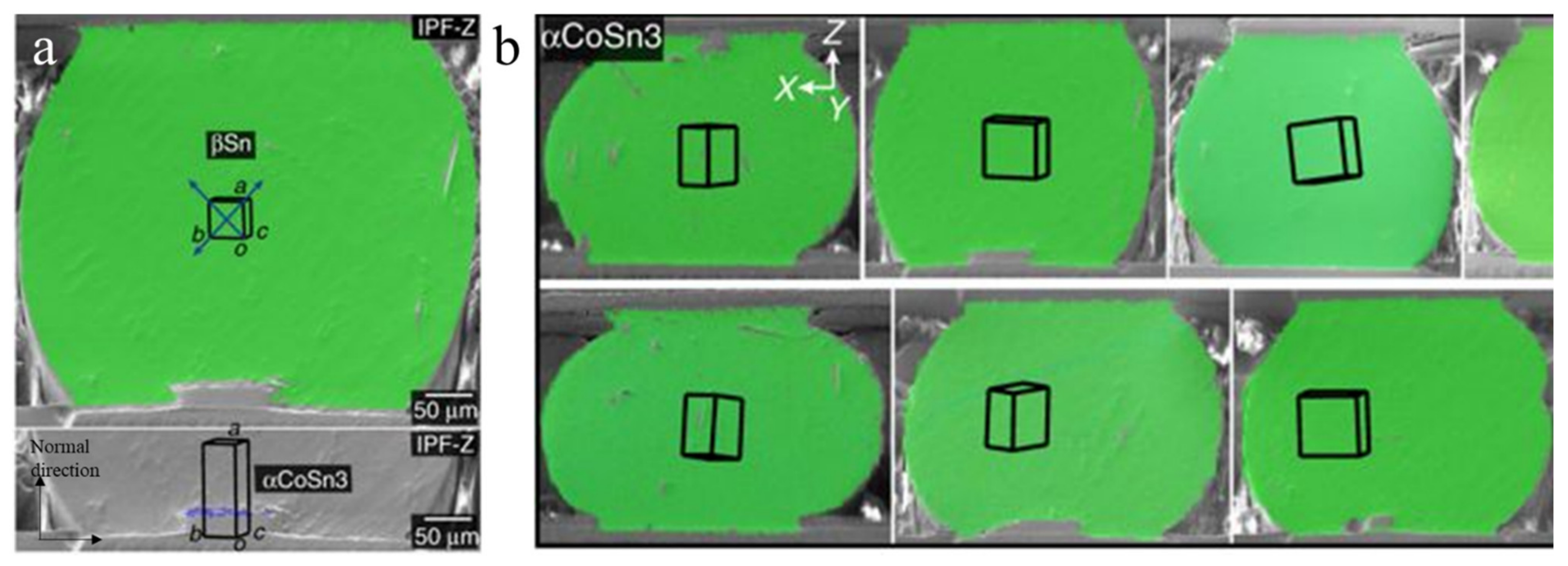
:1. Introduction
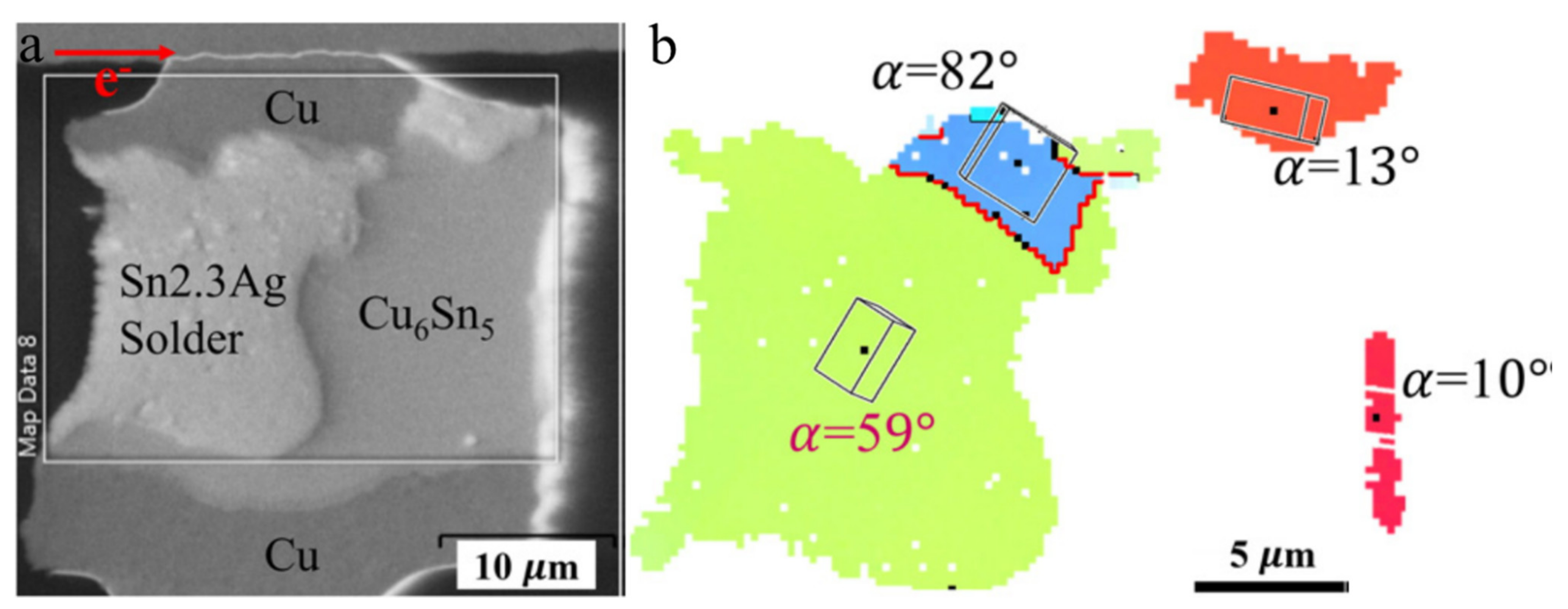
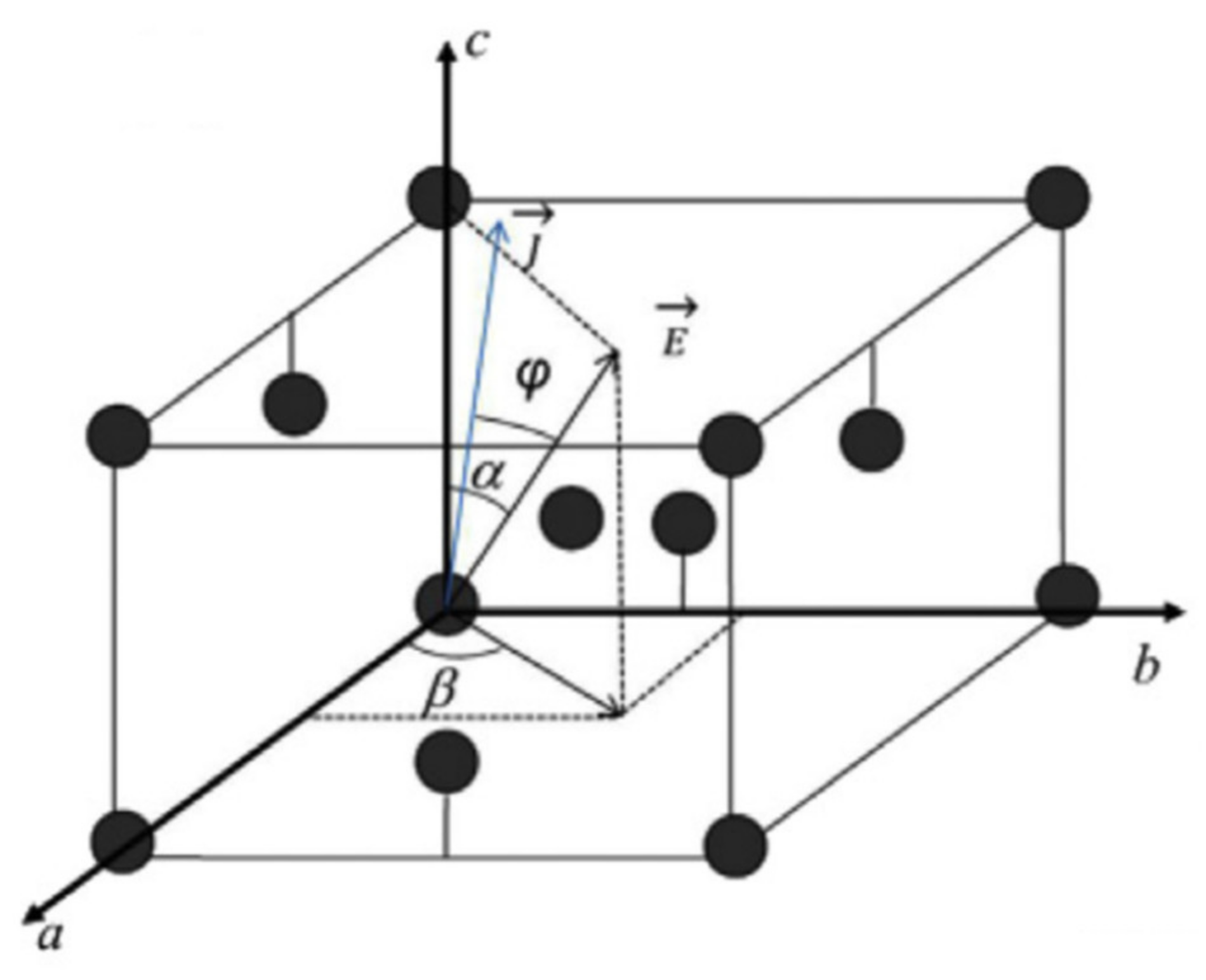
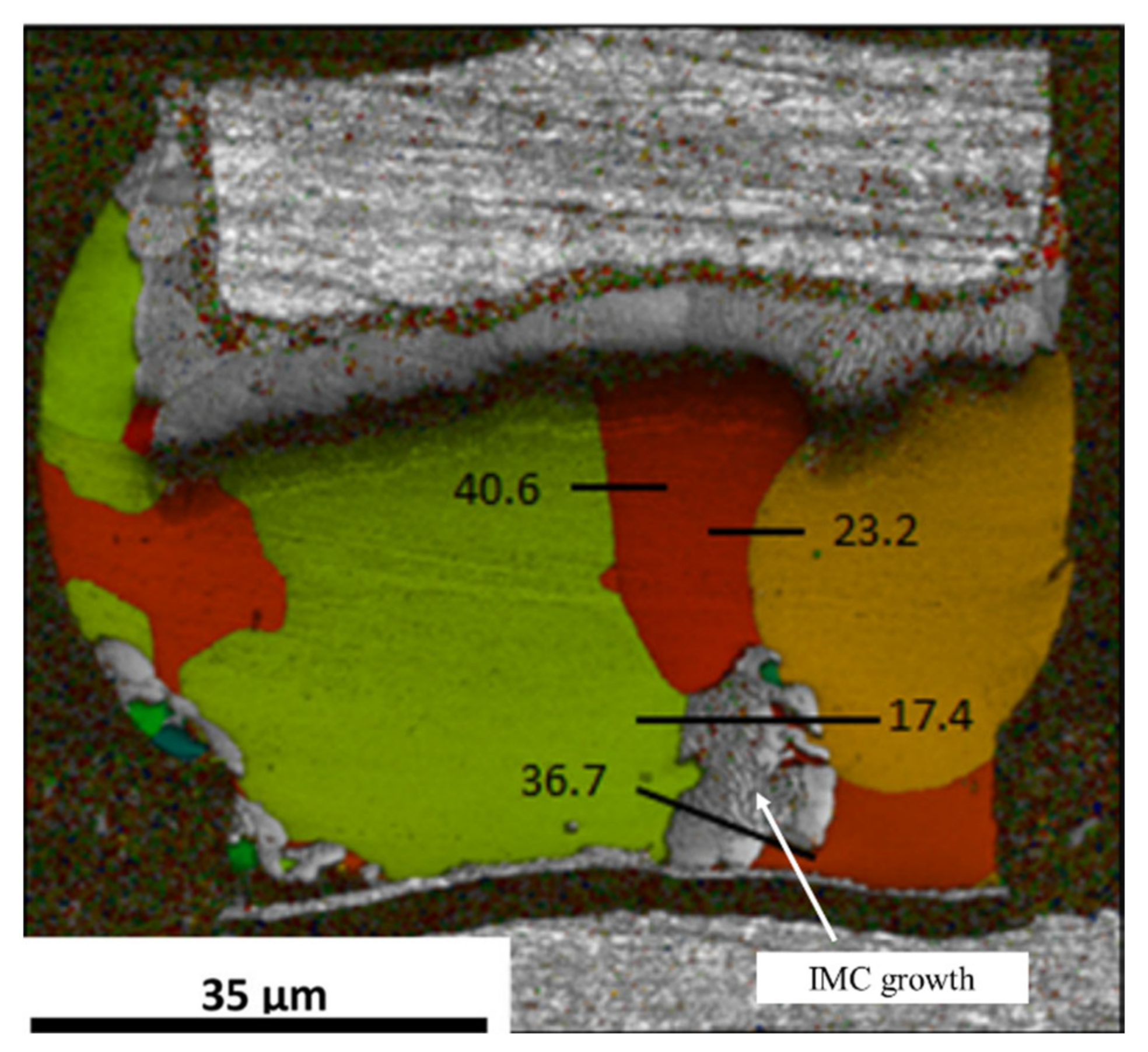
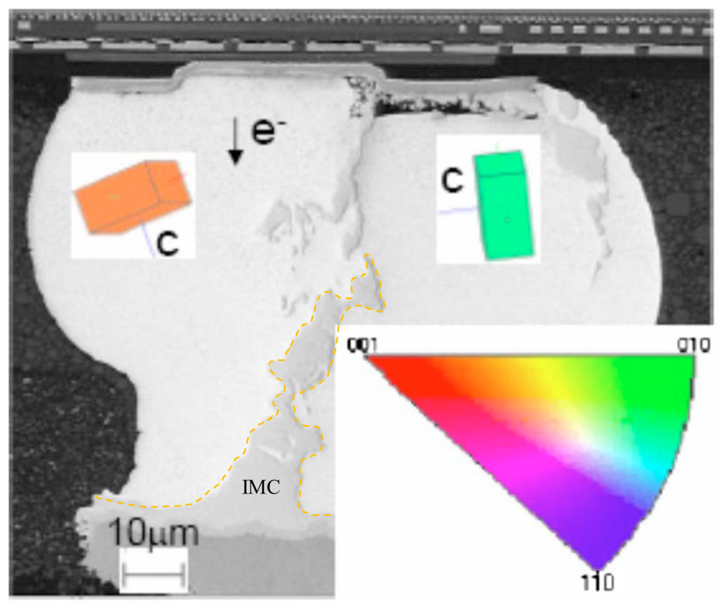
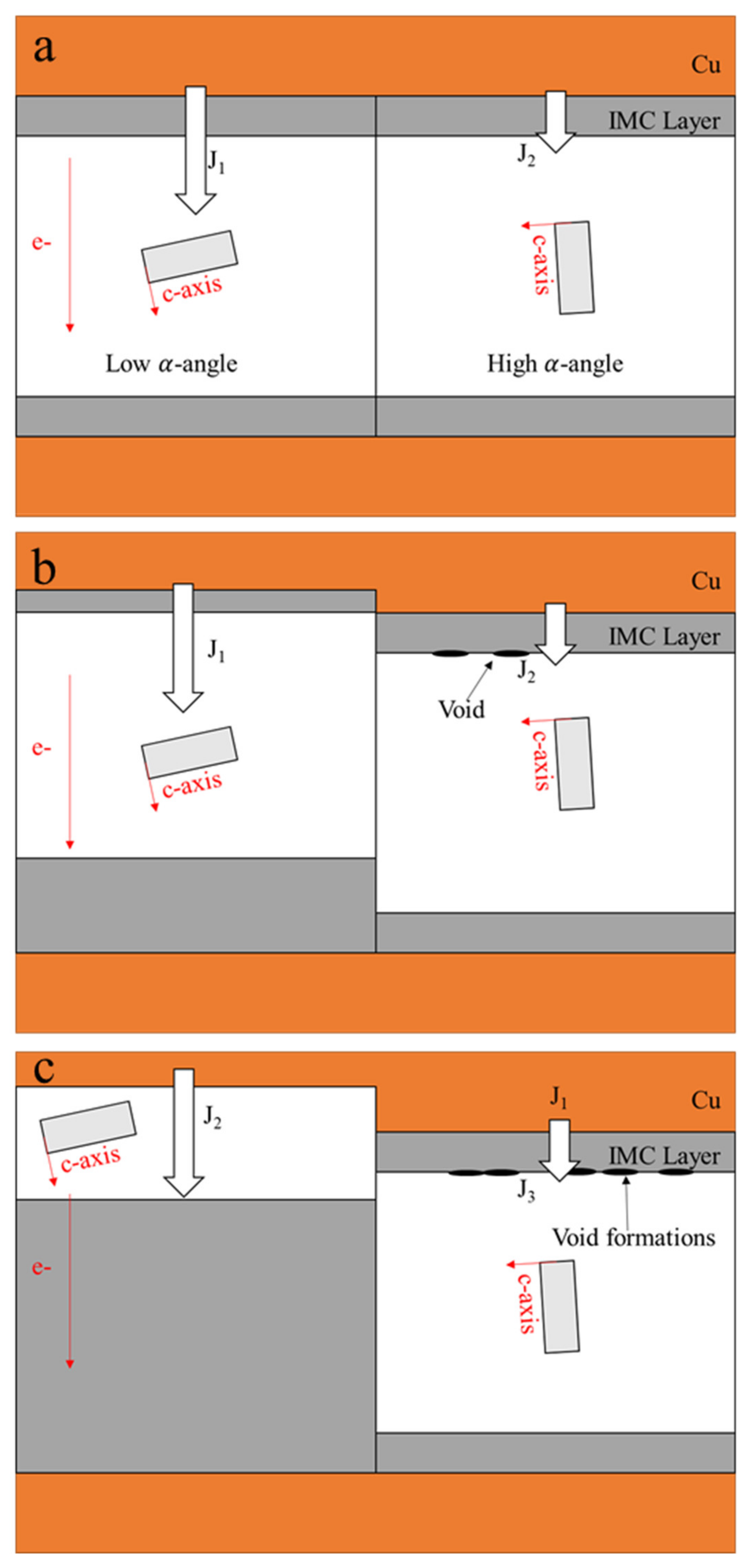
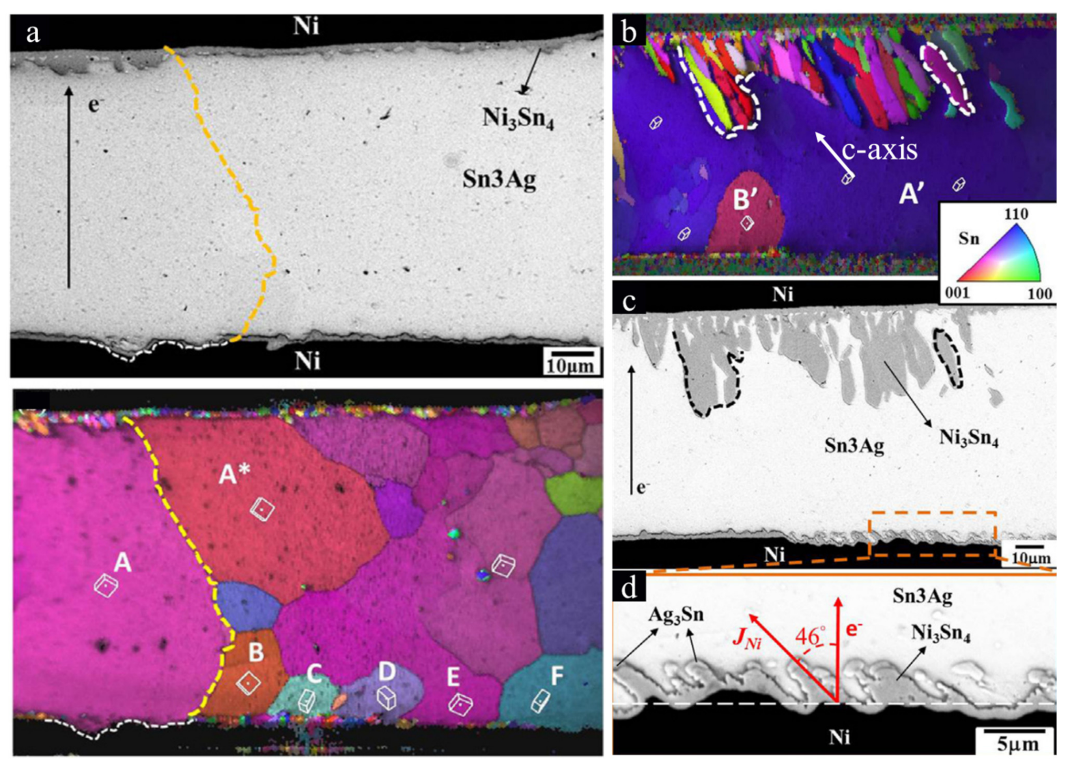
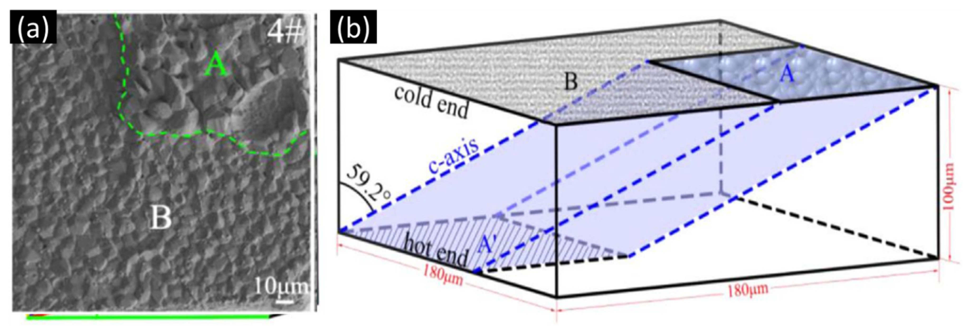
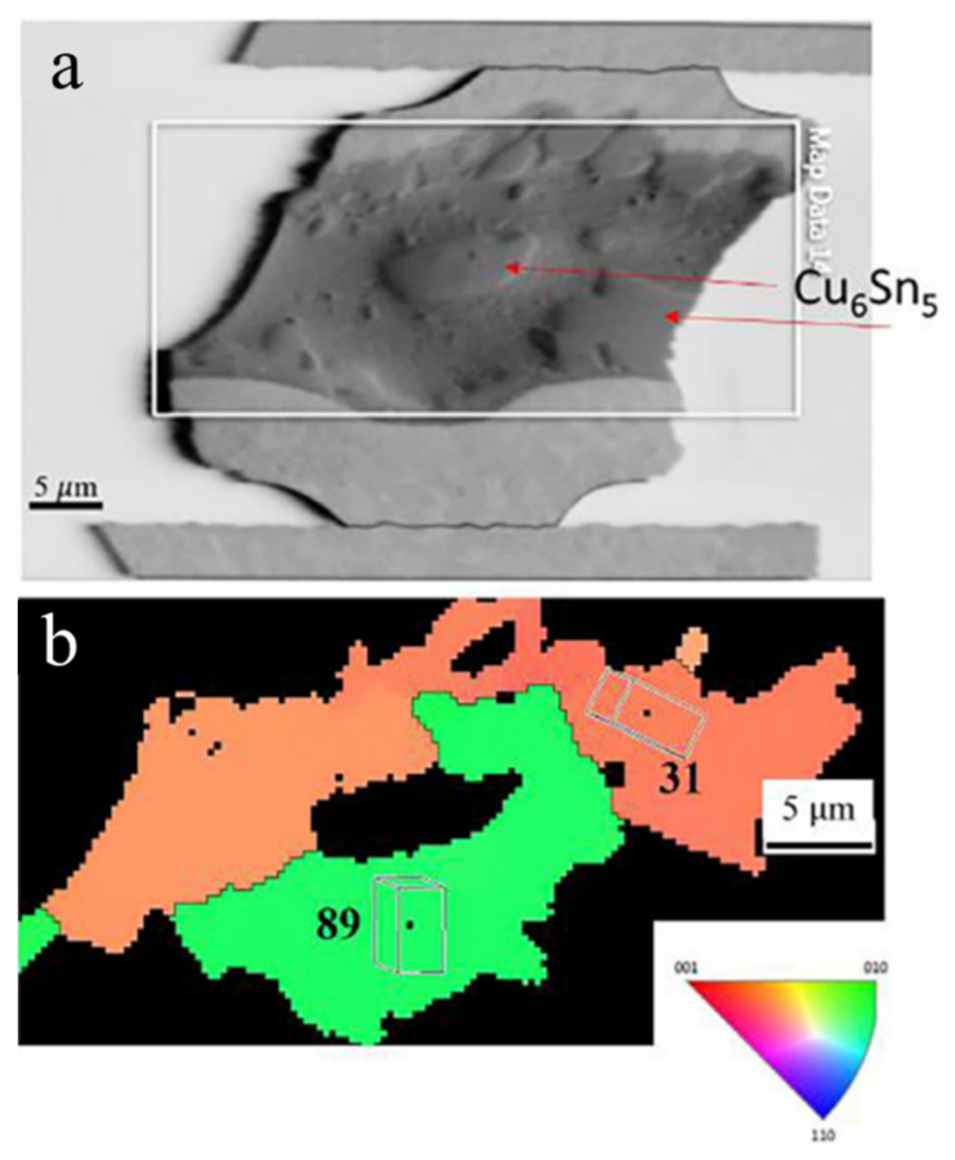
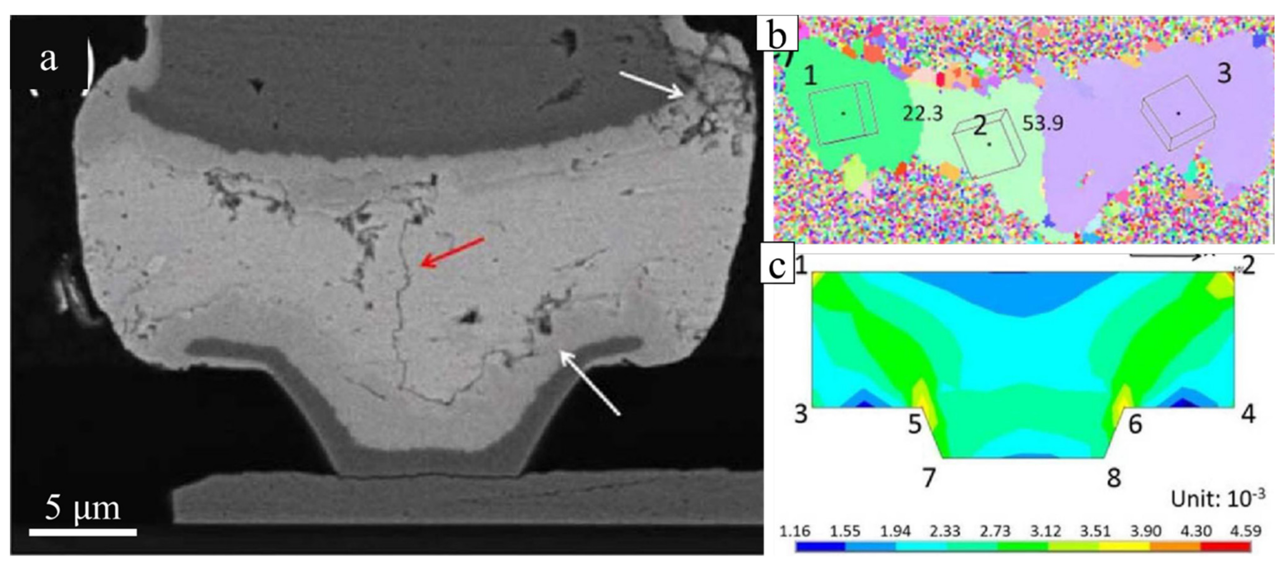
2. Effect of Sn Grain Orientation on Electromigration
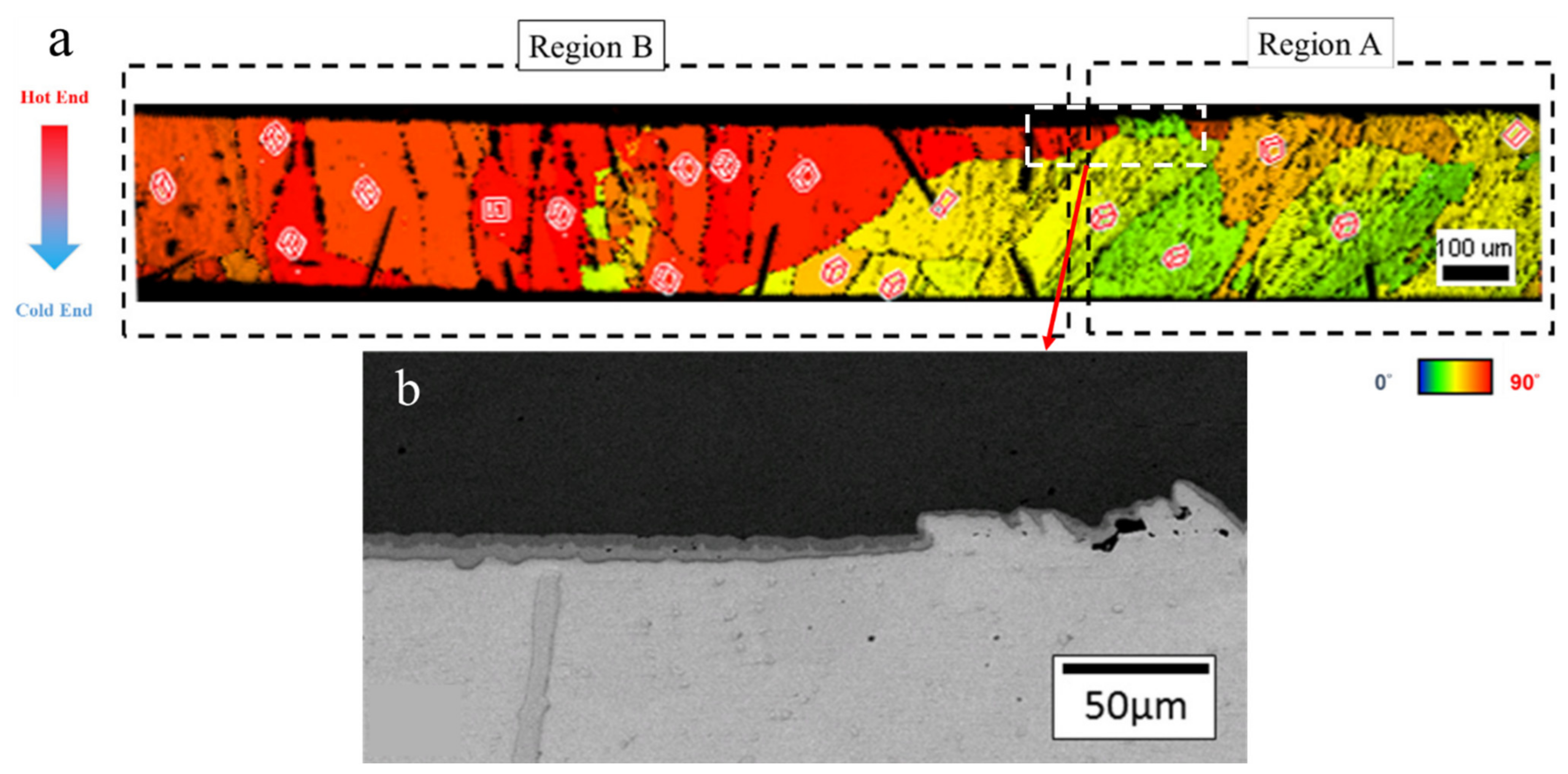
3. Effect of Sn Grain Orientation on Thermomigration
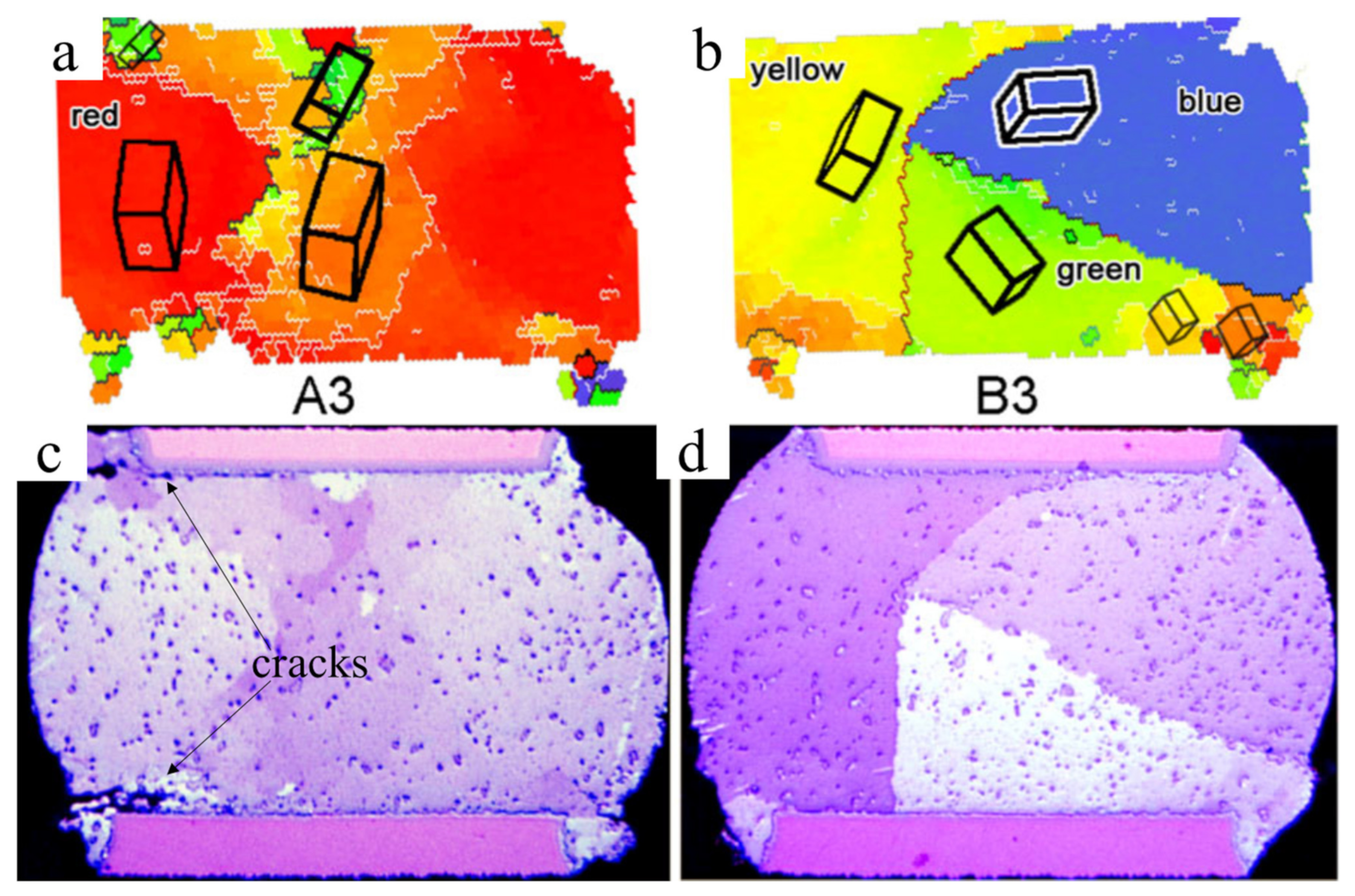
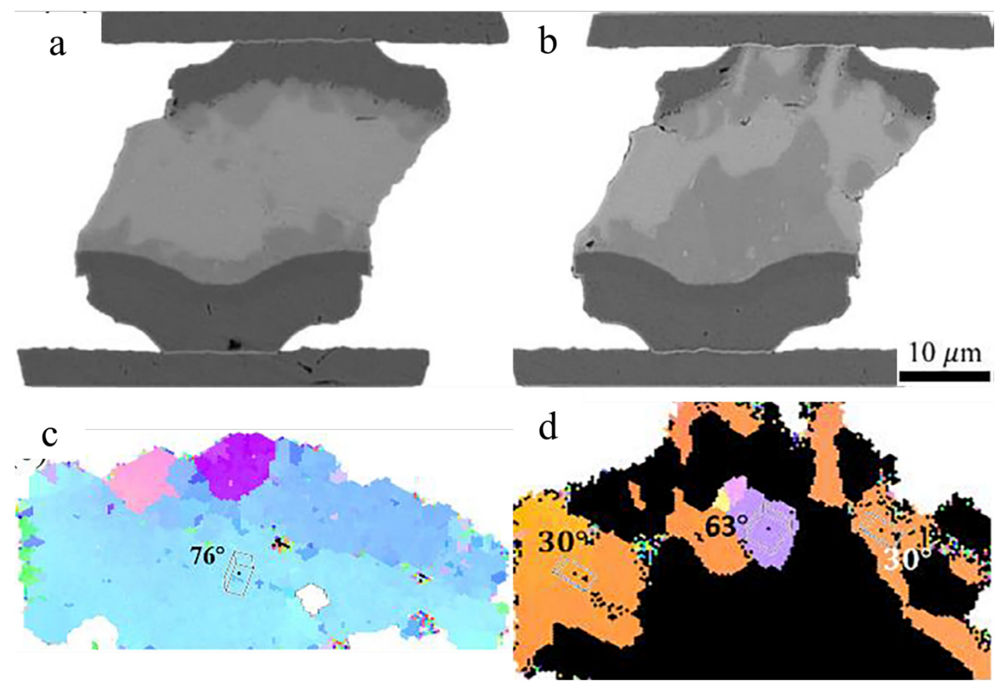
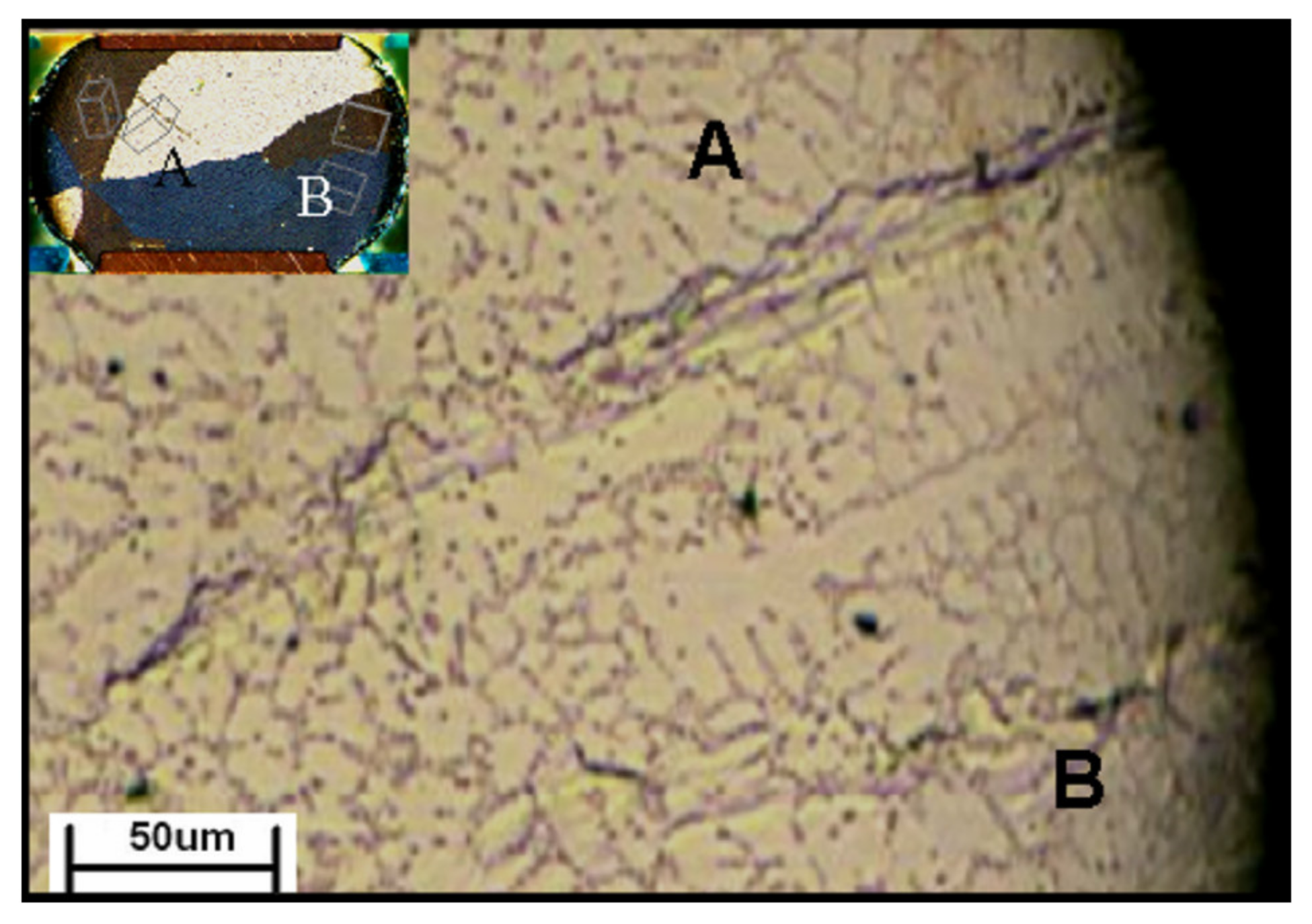
4. Effect of Sn Grain Orientation on Thermomechanical Fatigue
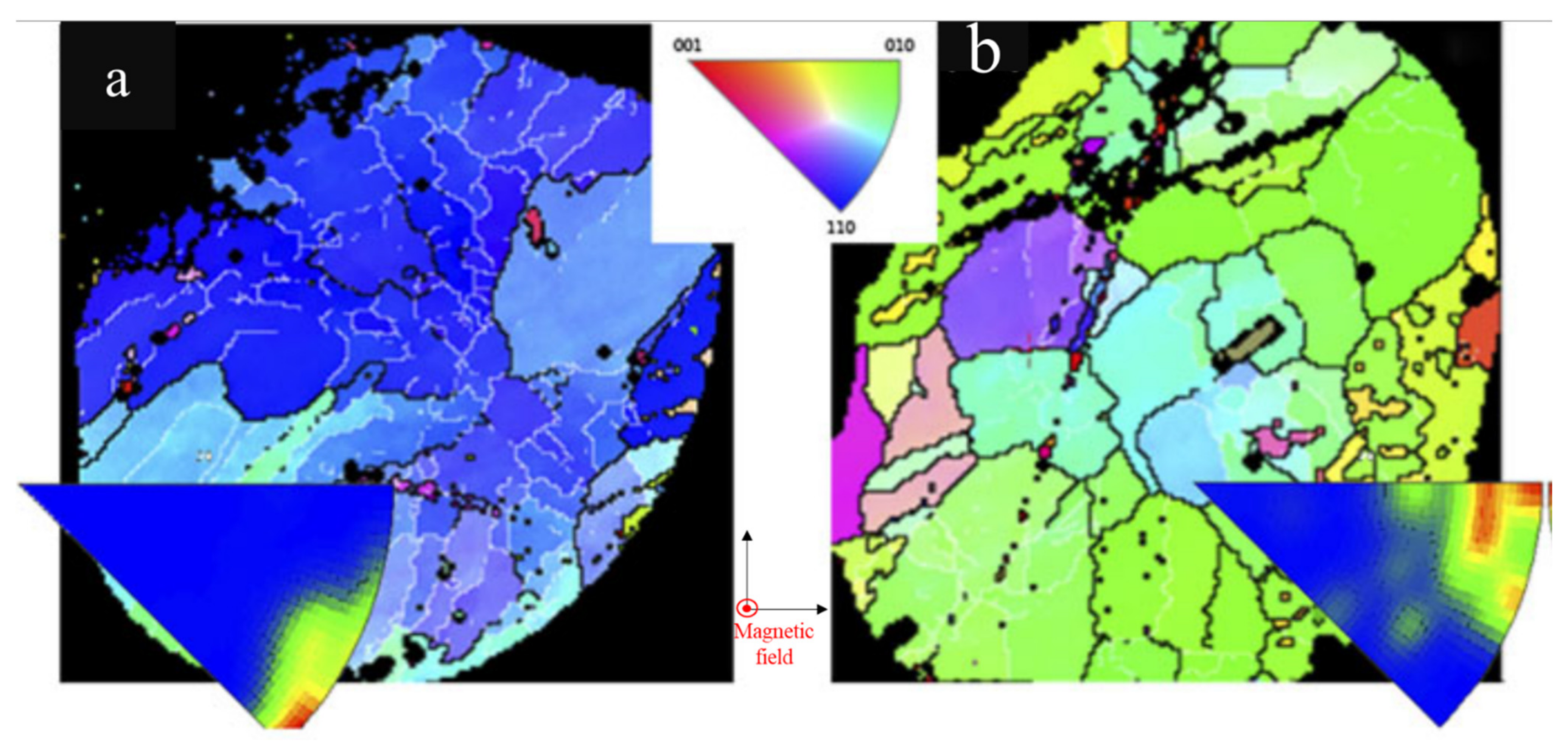
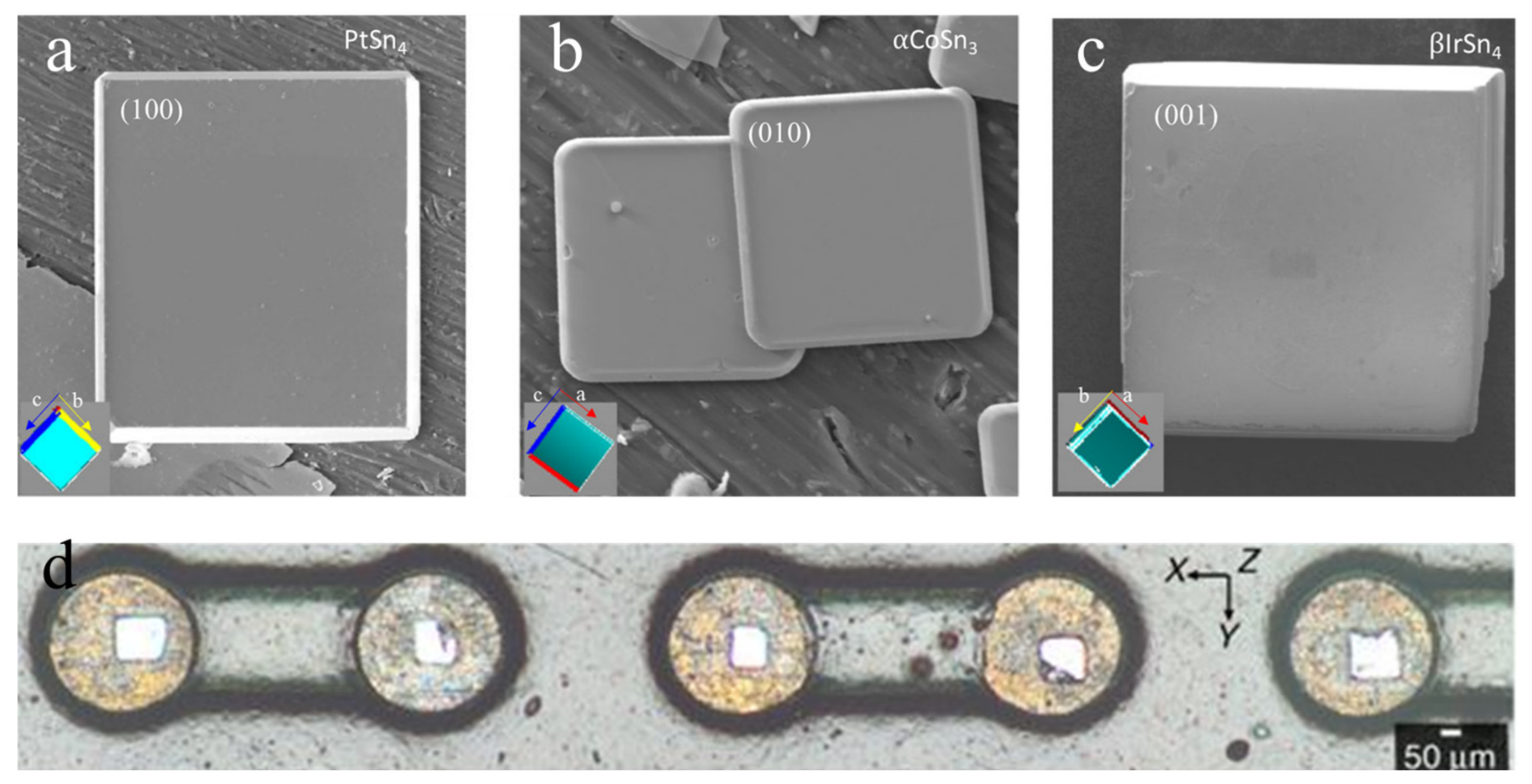
5. Method of Sn Grain-Orientation Control in Solder Joint
6. Summary
Author Contributions
Funding
Institutional Review Board Statement
Informed Consent Statement
Conflicts of Interest
References
- Abtew, M.; Selvaduray, G. Lead-Free Solders in Microelectronics. Mater. Sci. Eng. R Rep. 2000, 27, 95–141. [Google Scholar] [CrossRef]
- Suganuma, K. Advances in Lead-Free Electronics Soldering. Curr. Opin. Solid State Mater. Sci. 2001, 5, 55–64. [Google Scholar] [CrossRef]
- Subramanian, K.N. (Ed.) Preface; John Wiley and Sons, Ltd.: Chichester, UK, 2012; ISBN 9780470971826. [Google Scholar]
- Morris, J.W.; Goldstein, J.L.F.; Mei, Z. Microstructure and Mechanical Properties of Sn-In and Sn-Bi Solders. JOM 1993, 45, 25–27. [Google Scholar] [CrossRef]
- Yang, W.; Messler, R.W.; Felton, L.E. Microstructure Evolution of Eutectic Sn-Ag Solder Joints. J. Electron. Mater. 1994, 23, 765–772. [Google Scholar] [CrossRef]
- Lee, B.-J.; Oh, C.-S.; Shim, J.-H. Thermodynamic Assessments of the Sn-In and Sn-Bi Binary Systems. J. Electron. Mater. 1996, 25, 983–991. [Google Scholar] [CrossRef]
- Kim, K.S.; Huh, S.H.; Suganuma, K. Effects of Intermetallic Compounds on Properties of Sn–Ag–Cu Lead-Free Soldered Joints. J. Alloys Compd. 2003, 352, 226–236. [Google Scholar] [CrossRef]
- Gao, H.; Wei, F.; Sui, Y.; Qi, J. Growth Behaviors of Intermetallic Compounds on the Sn-0.7Cu-10Bi-XCo/Co Interface during Multiple Reflow. Mater. Des. 2019, 174, 107794. [Google Scholar] [CrossRef]
- Kolenak, R.; Kostolný, I.; Sahul, M. Direct Bonding of Silicon with Solders Type Sn-Ag-Ti. Solder. Surf. Mt. Technol. 2016, 28, 149–158. [Google Scholar] [CrossRef]
- Hou, Z.; Zhao, X.; Gu, Y.; Tan, C.; Huo, Y.; Li, H.; Shi, S.; Liu, Y. Enhancement Mechanism of Te Doping on Microstructure, Wettability and Mechanical Properties of Sn–Bi-Based Solder. Mater. Sci. Eng. A 2022, 848, 143445. [Google Scholar] [CrossRef]
- Korhonen, T.-M.; Kivilahti, J.K. Thermodynamics of the Sn-In-Ag Solder System. J. Electron. Mater. 1998, 27, 149–158. [Google Scholar] [CrossRef]
- Alam, M.O.; Chan, Y.C.; Tu, K.N. Effect of 0.5 Wt% Cu Addition in Sn–3.5%Ag Solder on the Dissolution Rate of Cu Metallization. J. Appl. Phys. 2003, 94, 7904. [Google Scholar] [CrossRef] [Green Version]
- Seo, S.-K.; Kang, S.K.; Shih, D.-Y.; Lee, H.M. An Investigation of Microstructure and Microhardness of Sn-Cu and Sn-Ag Solders as Functions of Alloy Composition and Cooling Rate. J. Electron. Mater. 2009, 38, 257–265. [Google Scholar] [CrossRef]
- Wu, C.M.L.; Yu, D.Q.; Law, C.M.T.; Wang, L. Properties of Lead-Free Solder Alloys with Rare Earth Element Additions. Mater. Sci. Eng. R Rep. 2004, 44, 1–44. [Google Scholar] [CrossRef]
- Shen, Y.-A.; Chen, H.-Z.; Chen, S.-W.; Chiu, S.-K.; Guo, X.-Y.; Hsieh, Y.-P. Graphene as a Diffusion Barrier at the Interface of Liquid–State Low-Melting Sn–58Bi Alloy and Copper Foil. Appl. Surf. Sci. 2022, 578, 152108. [Google Scholar] [CrossRef]
- Frear, D.R.; Jang, J.W.; Lin, J.K.; Zhang, C. Pb-Free Solders for Flip-Chip Interconnects. JOM 2001, 53, 28–33. [Google Scholar] [CrossRef]
- Zeng, K.; Tu, K.N. Six Cases of Reliability Study of Pb-Free Solder Joints in Electronic Packaging Technology. Mater. Sci. Eng. R Rep. 2002, 38, 55–105. [Google Scholar] [CrossRef]
- Shen, Y.-A.; Chen, S.-W.; Chen, H.-Z.; Chang, C.-M.; Ouyang, Y.-H. Extremely Thin Interlayer of Multi-Element Intermetallic Compound between Sn-Based Solders and FeCoNiMn High-Entropy Alloy. Appl. Surf. Sci. 2021, 558, 149945. [Google Scholar] [CrossRef]
- Tu, K.N. Recent Advances on Electromigration in Very-Large-Scale-Integration of Interconnects. J. Appl. Phys. 2003, 94, 5451–5473. [Google Scholar] [CrossRef]
- Meinshausen, L.; Weide-Zaage, K.; Frémont, H. Dynamical IMC-Growth Calculation. Microelectron. Reliab. 2015, 55, 1832–1837. [Google Scholar] [CrossRef]
- Chan, H.T.; Lin, C.F.; Yen, Y.W.; Chen, C.M. Effects of Current Stressing on the P-Bi2Te3/Sn Interfacial Reactions. J. Alloys Compd. 2016, 668, 91–96. [Google Scholar] [CrossRef]
- Chen, C.; Tong, H.M.; Tu, K.N. Electromigration and Thermomigration in Pb-Free Flip-Chip Solder Joints. Annu. Rev. Mater. Res. 2010, 40, 531–555. [Google Scholar] [CrossRef]
- Huang, M.L.; Zhang, Z.J.; Zhao, N.; Zhou, Q. A Synchrotron Radiation Real-Time in Situ Imaging Study on the Reverse Polarity Effect in Cu/Sn–9Zn/Cu Interconnect during Liquid–Solid Electromigration. Scr. Mater. 2013, 68, 853–856. [Google Scholar] [CrossRef]
- Chen, C.M.; Chen, S.W. Electromigration Effect upon the Sn/Ag and Sn/Ni Interfacial Reactions at Various Temperatures. Acta Mater. 2002, 50, 2461–2469. [Google Scholar] [CrossRef]
- Bashir, M.N.; Haseeb, A.S.M.A. Grain Size Stability of Interfacial Intermetallic Compound in Ni and Co Nanoparticle-Doped SAC305 Solder Joints under Electromigration. J. Mater. Sci. Mater. Electron. 2022, 33, 14240–14248. [Google Scholar] [CrossRef]
- Lin, Y.H.; Tsai, C.M.; Hu, Y.C.; Lin, Y.L.; Kao, C.R. Electromigration-Induced Failure in Flip-Chip Solder Joints. J. Electron. Mater. 2005, 34, 27–33. [Google Scholar] [CrossRef]
- Abdulhamid, M.F.; Basaran, C. Influence of Thermomigration on Lead-Free Solder Joint Mechanical Properties. J. Electron. Packag. 2009, 131, 011002. [Google Scholar] [CrossRef]
- Chen, C.; Hsiao, H.-Y.; Chang, Y.-W.; Ouyang, F.; Tu, K.N. Thermomigration in Solder Joints. Mater. Sci. Eng. R Rep. 2012, 73, 85–100. [Google Scholar] [CrossRef]
- Park, S.; Dhakal, R.; Lehman, L.; Cotts, E. Measurement of Deformations in SnAgCu Solder Interconnects under in Situ Thermal Loading. Acta Mater. 2007, 55, 3253–3260. [Google Scholar] [CrossRef]
- Matin, M.A.; Vellinga, W.P.; Geers, M.G.D. Thermomechanical Fatigue Damage Evolution in SAC Solder Joints. Mater. Sci. Eng. A 2007, 445–446, 73–85. [Google Scholar] [CrossRef]
- Ahat, S.; Sheng, M.; Luo, L. Effects of Static Thermal Aging and Thermal Cycling on the Microstructure and Shear Strength of Sn95.5Ag3.8Cu0.7 Solder Joints. J. Mater. Res. 2001, 16, 2914–2921. [Google Scholar] [CrossRef]
- Pearson, W.B. (Ed.) A Handbook of Lattice Spacings and Structures of Metals and Alloys; Elsevier: London, UK, 1958; ISBN 9781483213187. [Google Scholar]
- Dyson, B.F.; Anthony, T.R.; Turnbull, D. Interstitial Diffusion of Copper in Tin. J. Appl. Phys. 1967, 38, 3408. [Google Scholar] [CrossRef]
- Yeh, D.C.; Huntington, H.B. Extreme Fast-Diffusion System: Nickel in Single-Crystal Tin. Phys. Rev. Lett. 1984, 53, 1469–1472. [Google Scholar] [CrossRef]
- Rayne, J.A.; Chandrasekhar, B.S. Elastic Constants of β Tin from 4.2 °K to 300 °K. Phys. Rev. 1960, 120, 1658–1663. [Google Scholar] [CrossRef]
- Deshpande, V.T.; Sirdeshmukh, D.B. IUCr Thermal Expansion of Tin in the β–γ Transition Region. Acta Crystallogr. 1962, 15, 294–295. [Google Scholar] [CrossRef]
- Case, S.K.; Gueths, J.E. Anisotropy of the Temperature-Dependent Resistivity of Tin between 8 and 300 °K. Phys. Rev. B 1970, 2, 3843–3848. [Google Scholar] [CrossRef]
- Lee, B.-Z.; Lee, D.N. Spontaneous Growth Mechanism of Tin Whiskers. Acta Mater. 1998, 46, 3701–3714. [Google Scholar] [CrossRef]
- Ernst, B.; Keim, S.; Tetzlaff, U. On the Anisotropic Indentation Modulus and Anisotropic Creep Behavior of β-Sn Characterized by Nanoindentation Methods. Mater. Sci. Eng. A 2022, 848, 143392. [Google Scholar] [CrossRef]
- Tu, K.N. Reliability Challenges in 3D IC Packaging Technology. Microelectron. Reliab. 2011, 51, 517–523. [Google Scholar] [CrossRef]
- Chen, K.-N.; Tu, K.-N. Materials Challenges in Three-Dimensional Integrated Circuits. MRS Bull. 2015, 40, 219–222. [Google Scholar] [CrossRef] [Green Version]
- Huang, Y.T.; Hsu, H.H.; Wu, A.T. Electromigration-Induced Back Stress in Critical Solder Length for Three-Dimensional Integrated Circuits. J. Appl. Phys. 2014, 115, 034904. [Google Scholar] [CrossRef]
- Black, J.R. Electromigration Failure Modes in Aluminum Metallization for Semiconductor Devices. Proc. IEEE 1969, 57, 1587–1594. [Google Scholar] [CrossRef]
- Black, J.R. Electromigration—A Brief Survey and Some Recent Results. IEEE Trans. Electron Devices 1969, 16, 338–347. [Google Scholar] [CrossRef] [Green Version]
- Ho, P.S.; Kwok, T. Electromigration in Metals. Rep. Prog. Phys. 1989, 52, 301–348. [Google Scholar] [CrossRef]
- Lee, P.T.; Hsieh, W.Z.; Lee, C.Y.; Tseng, S.C.; Tang, M.T.; Chiang, C.Y.; Kao, C.R.; Ho, C.E. Synchrotron X-ray Study of Electromigration, Whisker Growth, and Residual Strain Evolution in a Sn Blech Structure. Scr. Mater. 2022, 214, 114682. [Google Scholar] [CrossRef]
- Jepiti, P.; Yoon, S.; Kim, J. Electromigration Reliability in Ag Lines Printed with Nanoparticle Inks: Implications for Printed Electronics. ACS Appl. Nano Mater. 2022, 5, 2569–2577. [Google Scholar] [CrossRef]
- Liu, Y.C.; Yu, Y.S.; Lin, S.K.; Chiu, S.J. Electromigration Effect upon Single- and Two-Phase Ag-Cu Alloy Strips: An In Situ Study. Scr. Mater. 2019, 173, 134–138. [Google Scholar] [CrossRef]
- Lu, M.; Shih, D.-Y.; Lauro, P.; Goldsmith, C.; Henderson, D.W. Effect of Sn Grain Orientation on Electromigration Degradation Mechanism in High Sn-Based Pb-Free Solders. Appl. Phys. Lett. 2008, 92, 211909. [Google Scholar] [CrossRef]
- Wang, Y.; Lu, K.H.; Gupta, V.; Stiborek, L.; Shirley, D.; Im, J.; Ho, P.S. Effect of Sn Grain Structure on Electromigration Reliability of Pb-Free Solders. In Proceedings of the 2011 IEEE 61st Electronic Components and Technology Conference (ECTC), Lake Buena Vista, FL, USA, 31 May–3 June 2011; pp. 711–716. [Google Scholar]
- Lee, K.; Kim, K.-S.; Tsukada, Y.; Suganuma, K.; Yamanaka, K.; Kuritani, S.; Ueshima, M. Effects of the Crystallographic Orientation of Sn on the Electromigration of Cu/Sn–Ag–Cu/Cu Ball Joints. J. Mater. Res. 2011, 26, 467–474. [Google Scholar] [CrossRef]
- Wang, Y.; Lu, K.H.; Gupta, V.; Stiborek, L.; Shirley, D.; Chae, S.-H.; Im, J.; Ho, P.S. Effects of Sn Grain Structure on the Electromigration of Sn–Ag Solder Joints. J. Mater. Res. 2012, 27, 1131–1141. [Google Scholar] [CrossRef]
- Wei, C.C.; Yu, C.H.; Tung, C.H.; Huang, R.Y.; Hsieh, C.C.; Chiu, C.C.; Hsiao, H.Y.; Chang, Y.W.; Lin, C.K.; Liang, Y.C.; et al. Comparison of the Electromigration Behaviors between Micro-Bumps and C4 Solder Bumps. In Proceedings of the Proceedings—Electronic Components and Technology Conference, Lake Buena Vista, FL, USA, 31 May–3 June 2011; pp. 706–710. [Google Scholar]
- Huang, M.L.; Zhao, J.F.; Zhang, Z.J.; Zhao, N. Role of Diffusion Anisotropy in β-Sn in Microstructural Evolution of Sn-3.0Ag-0.5Cu Flip Chip Bumps Undergoing Electromigration. Acta Mater. 2015, 100, 98–106. [Google Scholar] [CrossRef]
- Lin, C.F.; Lee, S.H.; Chen, C.M. Effect of Sn Grain Orientation on the Cu6Sn5 Formation in a Sn-Based Solder Under Current Stressing. Metall. Mater. Trans. A 2012, 43, 2571–2573. [Google Scholar] [CrossRef]
- Liu, C.Y.; Chen, C.; Mal, A.K.; Tu, K.N. Direct Correlation between Mechanical Failure and Metallurgical Reaction in Flip Chip Solder Joints. J. Appl. Phys. 1999, 85, 3882–3886. [Google Scholar] [CrossRef]
- Jang, J.W.; De Silva, A.P.; Lee, T.Y.; Lin, J.K.; Frear, D.R. Direct Correlation between Microstructure and Mechanical Tensile Properties in Pb-Free Solders and Eutectic SnPb Solder for Flip Chip Technology. Appl. Phys. Lett. 2001, 79, 482–484. [Google Scholar] [CrossRef]
- Ren, F.; Nah, J.-W.; Tu, K.N.; Xiong, B.; Xu, L.; Pang, J.H.L. Electromigration Induced Ductile-to-Brittle Transition in Lead-Free Solder Joints. Appl. Phys. Lett. 2006, 89, 141914. [Google Scholar] [CrossRef]
- Zhang, L.; Wang, Z.G.; Shang, J.K. Current-Induced Weakening of Sn3.5Ag0.7Cu Pb-Free Solder Joints. Scr. Mater. 2007, 56, 381–384. [Google Scholar] [CrossRef]
- Bashir, M.N.; Haseeb, A.S.M.A.; Rahman, A.Z.M.S.; Fazal, M.A.; Kao, C.R. Reduction of Electromigration Damage in SAC305 Solder Joints by Adding Ni Nanoparticles through Flux Doping. J. Mater. Sci. 2015, 50, 6748–6756. [Google Scholar] [CrossRef]
- Shen, Y.-A.; Chen, C. Effect of Sn Grain Orientation on Formation of Cu6Sn5 Intermetallic Compounds during Electromigration. Scr. Mater. 2017, 128, 6–9. [Google Scholar] [CrossRef]
- Yeh, E.C.C.; Choi, W.J.; Tu, K.N.; Elenius, P.; Balkan, H. Current-Crowding-Induced Electromigration Failure in Flip Chip Solder Joints. Appl. Phys. Lett. 2002, 80, 580–582. [Google Scholar] [CrossRef]
- Chang, Y.-W.; Cheng, Y.; Xu, F.; Helfen, L.; Tian, T.; Di Michiel, M.; Chen, C.; Tu, K.-N.; Baumbach, T. Study of Electromigration-Induced Formation of Discrete Voids in Flip-Chip Solder Joints by in-Situ 3D Laminography Observation and Finite-Element Modeling. Acta Mater. 2016, 117, 100–110. [Google Scholar] [CrossRef]
- Ahmed, M.T.; Motalab, M.; Suhling, J.C. Impact of Mechanical Property Degradation and Intermetallic Compound Formation on Electromigration-Oriented Failure of a Flip-Chip Solder Joint. J. Electron. Mater. 2020, 50, 233–248. [Google Scholar] [CrossRef]
- Jeong, H.; Lee, C.J.; Kim, J.H.; Son, J.Y.; Jung, S.B. Electromigration Behavior of Cu Core Solder Joints Under High Current Density. Electron. Mater. Lett. 2020, 16, 513–519. [Google Scholar] [CrossRef]
- Lee, K.; Kim, K.-S.; Suganuma, K. Influence of Indium Addition on Electromigration Behavior of Solder Joint. J. Mater. Res. 2011, 26, 2624–2631. [Google Scholar] [CrossRef]
- Ke, J.H.; Chuang, H.Y.; Shih, W.L.; Kao, C.R. Mechanism for Serrated Cathode Dissolution in Cu/Sn/Cu Interconnect under Electron Current Stressing. Acta Mater. 2012, 60, 2082–2090. [Google Scholar] [CrossRef]
- Huang, T.C.; Yang, T.L.; Ke, J.H.; Li, C.C.; Kao, C.R. Precipitation Induced by Diffusivity Anisotropy in Sn Grains under Electron Current Stressing. J. Alloys Compd. 2013, 555, 237–240. [Google Scholar] [CrossRef]
- Huang, T.C.; Yang, T.L.; Ke, J.H.; Hsueh, C.H.; Kao, C.R. Effects of Sn Grain Orientation on Substrate Dissolution and Intermetallic Precipitation in Solder Joints under Electron Current Stressing. Scr. Mater. 2014, 80, 37–40. [Google Scholar] [CrossRef]
- Chen, J.-Q.; Liu, K.-L.; Guo, J.-D.; Ma, H.-C.; Wei, S.; Shang, J.-K. Electromigration Anisotropy Introduced by Tin Orientation in Solder Joints. J. Alloys Compd. 2017, 703, 264–271. [Google Scholar] [CrossRef]
- Chen, J.-Q.; Guo, J.-D.; Liu, K.-L.; Shang, J.-K. Dependence of Electromigration Damage on Sn Grain Orientation in Sn–Ag–Cu Solder Joints. J. Appl. Phys. 2013, 114, 153509. [Google Scholar] [CrossRef]
- Wang, Y.; Wang, Y.; Ma, L.; Han, J.; Guo, F. IMC Growth Behavior along C-Axis of Sn Grain under Current Stressing. J. Mater. Sci. Mater. Electron. 2019, 29, 13180–13187. [Google Scholar] [CrossRef]
- Wang, Y.; Wang, Y.; Han, J.; Tan, S.; Guo, F. Effects of Sn Grain C-Axis on Electromigration in Cu Reinforced Composite Solder Joints. J. Mater. Sci. Mater. Electron. 2018, 29, 5954–5960. [Google Scholar] [CrossRef]
- Xu, K.; Fu, X.; Wang, X.; Fu, Z.; Yang, X.; Chen, S.; Shi, Y.; Huang, Y.; Chen, H. The Effect of Grain Orientation of β-Sn on Copper Pillar Solder Joints during Electromigration. Materials 2021, 15, 108. [Google Scholar] [CrossRef]
- Fu, X.; En, Y.; Zhou, B.; Chen, S.; Huang, Y.; He, X.; Chen, H.; Yao, R. Microstructure and Grain Orientation Evolution in SnPb/SnAgCu Interconnects Under Electrical Current Stressing at Cryogenic Temperature. Materials 2019, 12, 1593. [Google Scholar] [CrossRef] [PubMed] [Green Version]
- Groves, S.; Paul, W. Band Structure of Gray Tin. Phys. Rev. Lett. 1963, 11, 194. [Google Scholar] [CrossRef]
- Vincent, S.; Kleiven, D.; Lastra, J.M.G.; Chang, J.H. Thermodynamic Investigation of Phase Transformation in Sn Anode for Magnesium Batteries. APL Mater. 2022, 10, 071104. [Google Scholar] [CrossRef]
- Tasooji, A.; Lara, L.; Lee, K. Effect of Grain Boundary Misorientation on Electromigration in Lead-Free Solder Joints. J. Electron. Mater. 2014, 43, 4386–4394. [Google Scholar] [CrossRef] [Green Version]
- Li, S.; Basaran, C. Effective Diffusivity of Lead Free Solder Alloys. Comput. Mater. Sci. 2009, 47, 71–78. [Google Scholar] [CrossRef]
- Lehman, L.P.; Xing, Y.; Bieler, T.R.; Cotts, E.J. Cyclic Twin Nucleation in Tin-Based Solder Alloys. Acta Mater. 2010, 58, 3546–3556. [Google Scholar] [CrossRef]
- Shao, T.L.; Chen, Y.H.; Chiu, S.H.; Chen, C. Electromigration Failure Mechanisms for SnAg3.5 Solder Bumps on Ti/Cr-Cu/Cu and Ni(P)/Au Metallization Pads. J. Appl. Phys. 2004, 96, 4518–4524. [Google Scholar] [CrossRef]
- Su, Y.P.; Wu, C.S.; Ouyang, F.Y. Asymmetrical precipitation of Ag3Sn intermetallic compounds induced by thermomigration of Ag in Pb-free microbumps during solid-state aging. J. Electron. Mater. 2016, 45, 30–37. [Google Scholar] [CrossRef]
- Zhao, N.; Zhong, Y.; Huang, M.L.; Ma, H.T.; Dong, W. Growth Kinetics of Cu6Sn5 Intermetallic Compound at Liquid-Solid Interfaces in Cu/Sn/Cu Interconnects under Temperature Gradient. Sci. Rep. 2015, 5, 13491. [Google Scholar] [CrossRef] [Green Version]
- Hsu, W.N.; Ouyang, F.Y. Effects of Anisotropic β-Sn Alloys on Cu Diffusion under a Temperature Gradient. Acta Mater. 2014, 81, 141–150. [Google Scholar] [CrossRef]
- Zhao, N.; Zhong, Y.; Huang, M.L.; Dong, W.; Ma, H.T.; Wang, Y.P. In Situ Study on Interfacial Reactions of Cu/Sn–9Zn/Cu Solder Joints under Temperature Gradient. J. Alloys Compd. 2016, 682, 1–6. [Google Scholar] [CrossRef]
- Zhao, N.; Zhong, Y.; Dong, W.; Huang, M.L.; Ma, H.T.; Wong, C.P. Formation of Highly Preferred Orientation of β-Sn Grains in Solidified Cu/SnAgCu/Cu Micro Interconnects under Temperature Gradient Effect. Appl. Phys. Lett. 2017, 110, 093504. [Google Scholar] [CrossRef]
- Qiao, Y.; Ma, H.; Zhao, N. Diffusion Anisotropy Induced Uneven Regional Growth of Cu6Sn5 IMC in Cu/SAC305/Cu Micro Solder Joints under Temperature Gradient. J. Alloys Compd. 2021, 886, 161221. [Google Scholar] [CrossRef]
- Qiao, Y.; Ma, H.; Yu, F.; Zhao, N. Quasi-in-Situ Observation on Diffusion Anisotropy Dominated Asymmetrical Growth of Cu-Sn IMCs under Temperature Gradient. Acta Mater. 2021, 217, 117168. [Google Scholar] [CrossRef]
- Shen, Y.-A.; Ouyang, F.-Y.; Chen, C. Effect of Sn Grain Orientation on Growth of Cu-Sn Intermetallic Compounds during Thermomigration in Cu-Sn2.3Ag-Ni Microbumps. Mater. Lett. 2019, 236, 190–193. [Google Scholar] [CrossRef]
- Huang, M.L.; Zhao, J.F.; Zhang, Z.J.; Zhao, N. Dominant Effect of High Anisotropy in β-Sn Grain on Electromigration-Induced Failure Mechanism in Sn-3.0Ag-0.5Cu Interconnect. J. Alloys Compd. 2016, 678, 370–374. [Google Scholar] [CrossRef]
- Zhang, B.; Ding, H.; Sheng, X. Reliability Study of Board-Level Lead-Free Interconnections under Sequential Thermal Cycling and Drop Impact. Microelectron. Reliab. 2009, 49, 530–536. [Google Scholar] [CrossRef]
- Subramanian, K.N.; Lee, J.G. Effect of Anisotropy of Tin on Thermomechanical Behavior of Solder Joints. J. Mater. Sci. Mater. Electron. 2004, 15, 235–240. [Google Scholar] [CrossRef]
- Lee, J.G.; Guo, F.; Choi, S.; Subramanian, K.N.; Bieler, T.R.; Lucas, J.P. Residual-Mechanical Behavior of Thermomechanically Fatigued Sn-Ag Based Solder Joints. J. Electron. Mater. 2002, 31, 946–952. [Google Scholar] [CrossRef]
- Yoshida, A.; Taniguchi, J.; Murata, K.; Kada, M.; Yamamoto, Y.; Takagi, Y.; Notomi, T.; Fujita, A. A Study on Package Stacking Process for Package-on-Package (PoP). In Proceedings of the 56th Electronic Components and Technology Conference 2006, San Diego, CA, USA, 30 May–2 June 2006; pp. 825–830. [Google Scholar] [CrossRef]
- Dutta, I.; Pan, D.; Marks, R.A.; Jadhav, S.G. Effect of Thermo-Mechanically Induced Microstructural Coarsening on the Evolution of Creep Response of SnAg-Based Microelectronic Solders. Mater. Sci. Eng. A 2005, 410–411, 48–52. [Google Scholar] [CrossRef]
- Lee, J.G.; Subramanian, K.N. Effect of Dwell Times on Thermomechanical Fatigue Behavior of Sn-Ag-Based Solder Joints. J. Electron. Mater. 2003, 32, 523–530. [Google Scholar] [CrossRef]
- Bieler, T.R.; Jiang, H.; Lehman, L.P.; Kirkpatrick, T.; Cotts, E.J.; Nandagopal, B. Influence of Sn Grain Size and Orientation on the Thermomechanical Response and Reliability of Pb-Free Solder Joints. IEEE Trans. Compon. Packag. Technol. 2008, 31, 370–381. [Google Scholar] [CrossRef]
- Ben Romdhane, E.; Roumanille, P.; Guédon-Gracia, A.; Pin, S.; Nguyen, P.; Frémont, H. From Early Microstructural Evolution to Intergranular Crack Propagation in SAC Solders under Thermomechanical Fatigue. Microelectron. Reliab. 2021, 126, 114288. [Google Scholar] [CrossRef]
- Bieler, T.R.; Zhou, B.; Blair, L.; Zamiri, A.; Darbandi, P.; Pourboghrat, F.; Lee, T.-K.; Liu, K.-C. The Role of Elastic and Plastic Anisotropy of Sn in Recrystallization and Damage Evolution During Thermal Cycling in SAC305 Solder Joints. J. Electron. Mater. 2012, 41, 283–301. [Google Scholar] [CrossRef]
- Lovberg, A.; Tegehall, P.E.; Wetter, G.; Brinkfeldt, K.; Andersson, D. Simulations of the Impact of Single-Grained Lead-Free Solder Joints on the Reliability of Ball Grid Array Components. In Proceedings of the 2017 18th International Conference on Thermal, Mechanical and Multi-Physics Simulation and Experiments in Microelectronics and Microsystems (EuroSimE), Dresden, Germany, 3–5 April 2017. [Google Scholar] [CrossRef]
- Lovberg, A.; Tegehall, P.E. The Stress State of BGA Solder Joints Influenced by the Grain Orientations of Neighboring Joints. In Proceedings of the 2018 IEEE 68th Electronic Components and Technology Conference (ECTC), San Diego, CA, USA, 29 May–1 June 2018; pp. 882–889. [Google Scholar] [CrossRef]
- Chu, Y.C.; Chen, C.; Kao, N.; Jiang, D.S. Effect of Sn Grain Orientation and Strain Distribution in 20-Μm-Diameter Microbumps on Crack Formation under Thermal Cycling Tests. Electron. Mater. Lett. 2017, 13, 457–462. [Google Scholar] [CrossRef]
- Asai, S.; Sassa, K.; Tahashi, M. Crystal Orientation of Non-Magnetic Materials by Imposition of a High Magnetic Field. Sci. Technol. Adv. Mater. 2003, 4, 455–460. [Google Scholar] [CrossRef] [Green Version]
- Li, S.; Wu, C.; Sassa, K.; Asai, S. The Control of Crystal Orientation in Ceramics by Imposition of a High Magnetic Field. Mater. Sci. Eng. A 2006, 422, 227–231. [Google Scholar] [CrossRef]
- Chen, J.-Q.; Guo, J.-D.; Ma, H.-C.; Liu, K.-L.; Zhu, Q.; Shang, J.K. Magnetic-Field Induced Anisotropy in Electromigration Behavior of Sn–Ag–Cu Solder Interconnects. J. Mater. Res. 2015, 30, 1065–1071. [Google Scholar] [CrossRef]
- Drienovsky, M.; Palcut, M.; Priputen, P.; Cuninková, E.; Bošák, O.; Kubliha, M.; Trnková, L.R. Properties of Sn-Ag-Cu Solder Joints Prepared by Induction Heating. Adv. Mater. Sci. Eng. 2020, 2020, 1724095. [Google Scholar] [CrossRef] [Green Version]
- Murygin, A.V.; Tynchenko, V.S.; Laptenok, V.D.; Emilova, O.A.; Bocharov, A.N. Complex of Automated Equipment and Technologies for Waveguides Soldering Using Induction Heating. IOP Conf. Ser. Mater. Sci. Eng. 2017, 173, 012023. [Google Scholar] [CrossRef] [Green Version]
- Ma, Z.L.; Belyakov, S.A.; Sweatman, K.; Nishimura, T.; Nishimura, T.; Gourlay, C.M. Harnessing Heterogeneous Nucleation to Control Tin Orientations in Electronic Interconnections. Nat. Commun. 2017, 8, 1916. [Google Scholar] [CrossRef] [PubMed]
- Ma, Z.L.; Xian, J.W.; Belyakov, S.A.; Gourlay, C.M. Nucleation and Twinning in Tin Droplet Solidification on Single Crystal Intermetallic Compounds. Acta Mater. 2018, 150, 281–294. [Google Scholar] [CrossRef]


Publisher’s Note: MDPI stays neutral with regard to jurisdictional claims in published maps and institutional affiliations. |
© 2022 by the authors. Licensee MDPI, Basel, Switzerland. This article is an open access article distributed under the terms and conditions of the Creative Commons Attribution (CC BY) license (https://creativecommons.org/licenses/by/4.0/).
Share and Cite
Shen, Y.-A.; Wu, J.A. Effect of Sn Grain Orientation on Reliability Issues of Sn-Rich Solder Joints. Materials 2022, 15, 5086. https://doi.org/10.3390/ma15145086
Shen Y-A, Wu JA. Effect of Sn Grain Orientation on Reliability Issues of Sn-Rich Solder Joints. Materials. 2022; 15(14):5086. https://doi.org/10.3390/ma15145086
Chicago/Turabian StyleShen, Yu-An, and John A. Wu. 2022. "Effect of Sn Grain Orientation on Reliability Issues of Sn-Rich Solder Joints" Materials 15, no. 14: 5086. https://doi.org/10.3390/ma15145086
APA StyleShen, Y.-A., & Wu, J. A. (2022). Effect of Sn Grain Orientation on Reliability Issues of Sn-Rich Solder Joints. Materials, 15(14), 5086. https://doi.org/10.3390/ma15145086