
Colossal Permittivity Characteristics of (Nb, Si) Co-Doped TiO2 Ceramics

 ,
,  , ,
, ,  and
and
Abstract
:1. Introduction
2. Experiment Procedure
2.1. Materials
2.2. Synthesis of (Nb0.5Si0.5)xTi1−xO2 Ceramics
2.3. Characterization Methods
3. Results and Discussion
4. Conclusions
Author Contributions
Funding
Institutional Review Board Statement
Informed Consent Statement
Data Availability Statement
Acknowledgments
Conflicts of Interest
References
- Chen, H.; Zhu, W.; Zhang, Z.; Cai, W.; Zhou, X. Er and Mg co-doped TiO2 nanorod arrays and improvement of photovoltaic property in perovskite solar cell. J. Alloys Compd. 2018, 771, 649–657. [Google Scholar] [CrossRef]
- Fan, J.; Cheng, Y.; Zheng, L.; Tong, L.; Hu, Z.; He, G. Giant dielectric response and relaxation behavior in (Tm + Ta) co-doped TiO2 ceramics. Phys. Chem. Chem. Phys. 2022, 24, 4759–4768. [Google Scholar] [CrossRef] [PubMed]
- Siriya, P.; Chanlek, N.; Srepusharawoot, P.; Thongbai, P. Excellent giant dielectric properties over wide temperatures of (Al, Sc)3+ and Nb5+ doped TiO. Results Phys. 2022, 36, 105458. [Google Scholar] [CrossRef]
- Siriya, P.; Pengpad, A.; Srepusharawoot, P.; Chanlek, N.; Thongbai, P. Improved microstructure and significantly enhanced dielectric properties of Al(3+)/Cr(3+)/Ta(5+) triple-doped TiO2 ceramics by Re-balancing charge compensation. RSC Adv. 2022, 12, 4946–4954. [Google Scholar] [CrossRef]
- Thanamoon, N.; Chanlek, N.; Moontragoon, P.; Srepusharawoot, P.; Thongbai, P. Microstructure, low loss tangent, and excellent temperature stability of Tb+Sb-doped TiO2 with high dielectric permittivity. Results Phys. 2022, 37, 105536. [Google Scholar] [CrossRef]
- Wang, Z.; Peng, P.; Zhang, L.; Wang, N.; Tang, B.; Cui, B.; Liu, J.; Xu, D. Effect of electric field on the microstructure and electrical properties of (In + Ta) co-doped TiO2 colossal dielectric ceramics. J. Mater. Sci. Mater. Electron. 2022, 33, 6283–6293. [Google Scholar] [CrossRef]
- Hu, W.; Liu, Y.; Withers, R.; Frankcombe, T.J.; Norén, L.; Snashall, A.; Kitchin, M.; Smith, P.; Gong, B.; Chen, H.; et al. Electron-pinned defect-dipoles for high-performance colossal permittivity materials. Nat. Mater. 2013, 12, 821–826. [Google Scholar] [CrossRef]
- Mandal, S.; Pal, S.; Kundu, A.K.; Menon, K.S.R.; Hazarika, A.; Rioult, M.; Belkhou, R. Direct view at colossal permittivity in donor-acceptor (Nb, In) co-doped rutile TiO2. Appl. Phys. Lett. 2016, 109, 092906. [Google Scholar] [CrossRef]
- Tsuji, K.; Han, H.; Guillemet-Fritsch, S.; Randall, C.A. Dielectric relaxation and localized electron hopping in colossal dielectric (Nb,In)-doped TiO2 rutile nanoceramics. Phys. Chem. Chem. Phys. 2017, 19, 8568–8574. [Google Scholar] [CrossRef] [Green Version]
- Zhao, L.; Wang, J.; Gai, Z.; Li, J.; Liu, J.; Wang, J.; Wang, C.; Wang, X. Annealing effects on the structural and dielectric properties of (Nb + In) co-doped rutile TiO2 ceramics. RSC Adv. 2019, 9, 8364–8368. [Google Scholar] [CrossRef] [Green Version]
- Sinclair, D.C.; Adams, T.B.; Morrison, F.; West, A. CaCu3Ti4O12: One-step internal barrier layer capacitor. Appl. Phys. Lett. 2002, 80, 2153–2155. [Google Scholar] [CrossRef]
- Adams, T.; Sinclair, D.; West, A. Giant Barrier Layer Capacitance Effects in CaCu3Ti4O12 Ceramics. Adv. Mater. 2002, 14, 1321–1323. [Google Scholar] [CrossRef]
- Mingmuang, Y.; Chanlek, N.; Thongbai, P. Ultra–Low Loss Tangent and Giant Dielectric Permittivity with Excellent Temperature Stability of TiO2 Co-Doped with Isovalent-Zr4+/Pentavalent-Ta5+ Ions. J. Mater. 2022, in press. [Google Scholar] [CrossRef]
- Yang, C.; Wei, X.; Hao, J. Colossal permittivity in TiO2 co-doped by donor Nb and isovalent Zr. J. Am. Ceram. Soc. 2017, 101, 307–315. [Google Scholar] [CrossRef]
- Kim, K.-M.; Kim, S.-J.; Lee, J.-H.; Kim, D.-Y. Microstructural evolution and dielectric properties of SiO2-doped CaCu3Ti4O12 ceramics. J. Eur. Ceram. Soc. 2007, 27, 3991–3995. [Google Scholar] [CrossRef]
- Kotb, H.M.; Ahmad, M.M.; Alraheem, N.A. Study of the structural, impedance spectroscopy and dielectric properties of Na and Si co-doped NiO ceramics. J. Phys. D Appl. Phys. 2017, 50, 435304. [Google Scholar] [CrossRef] [Green Version]
- Peng, P.; Chen, C.; Cui, B.; Li, J.; Xu, D.; Tang, B. Influence of the electric field on flash-sintered (Zr + Ta) co-doped TiO2 colossal permittivity ceramics. Ceram. Int. 2021, 48, 6016–6023. [Google Scholar] [CrossRef]
- Cheng, X.; Li, Z.; Wu, J. Colossal permittivity in ceramics of TiO2 Co-doped with niobium and trivalent cation. J. Mater. Chem. A 2015, 3, 5805–5810. [Google Scholar] [CrossRef]
- Song, Y.-C.; Liu, P.; Zhao, X.; Guo, B.; Cui, X. Dielectric properties of (Bi0.5Nb0.5) Ti1-O2 ceramics with colossal permittivity. J. Alloys Compd. 2017, 722, 676–682. [Google Scholar] [CrossRef]
- Hanaor, D.A.H.; Sorrell, C.C. Review of the anatase to rutile phase transformation. J. Mater. Sci. 2010, 46, 855–874. [Google Scholar] [CrossRef] [Green Version]
- Tuichai, W.; Danwittayakul, S.; Manyam, J.; Chanlek, N.; Takesada, M.; Thongbai, P. Giant dielectric properties of Ga3+–Nb5+ Co-doped TiO2 ceramics driven by the internal barrier layer capacitor effect. Materialia 2021, 18, 101175. [Google Scholar] [CrossRef]
- Zhao, X.-G.; Liu, P. Dielectric and electric relaxations induced by the complex defect clusters in (Yb+Nb) co-doped rutile TiO2 ceramics. J. Am. Ceram. Soc. 2017, 100, 3505–3513. [Google Scholar] [CrossRef]
- Wurst, J.C.; Nelson, J.A. Lineal Intercept Technique for Measuring Grain Size in Two-Phase Polycrystalline Ceramics. J. Am. Ceram. Soc. 1972, 55, 109. [Google Scholar] [CrossRef]
- Chen, G.-H.; Li, J.-L.; Chen, X.; Kang, X.-L.; Yuan, C.-L. Sintering temperature dependence of varistor properties and impedance spectroscopy behavior in ZnO based varistor ceramics. J. Mater. Sci. Mater. Electron. 2015, 26, 2389–2396. [Google Scholar] [CrossRef]
- Wang, X.W.; Zheng, Y.P.; Liang, B.K.; Zhang, G.; Shi, Y.C.; Zhang, B.H.; Xue, L.L.; Shang, S.Y.; Shang, J.; Yin, S.Q.; et al. Preparation and properties of La and Nb co-doped TiO2 colossal dielectric ceramic materials. J. Mater. Sci. Mater. Electron. 2020, 31, 16044–16052. [Google Scholar] [CrossRef]
- Jiao, L.; Guo, P.; Kong, D.; Huang, X.; Li, H. Dielectric properties of (Yb0.5Ta0.5)xTi1−xO2 ceramics with colossal permittivity and low dielectric loss. J. Mater. Sci. Mater. Electron. 2020, 31, 3654–3661. [Google Scholar] [CrossRef]
- Garai, M.; Reka, A.A.; Karmakara, B.; Mollaa, A.R. Microstructure–mechanical properties of Ag°/Au° doped K–Mg–Al–Si–O–F glass-ceramics. RSC Adv. 2021, 11, 11415–11424. [Google Scholar] [CrossRef]
- Wang, Z.; Chen, H.; Wang, T.; Xiao, Y.; Nian, W.; Fan, J. Enhanced relative permittivity in niobium and europium co-doped TiO2 ceramics. J. Eur. Ceram. Soc. 2018, 38, 3847–3852. [Google Scholar] [CrossRef]
- Thongyong, N.; Chanlek, N.; Srepusharawoot, P.; Thongbai, P. Origins of Giant Dielectric Properties with Low Loss Tangent in Rutile (Mg1/3Ta2/3)0.01Ti0.99O2 Ceramic. Molecules 2021, 26, 6952. [Google Scholar] [CrossRef]
- Fan, J.; Long, Z.; Hu, Z. Interface effects and defect clusters inducing thermal stability and giant dielectric response in (Ta+Y)-co-doped TiO2 ceramics. J. Mater. Sci. Mater. Electron. 2021, 32, 26232–26240. [Google Scholar] [CrossRef]
- Fan, J.; Long, Z.; Zhou, H.; He, G.; Hu, Z. Colossal dielectric behavior of (Ho, Ta) co-doped rutile TiO2 ceramics. J. Mater. Sci. Mater. Electron. 2021, 32, 14780–14790. [Google Scholar] [CrossRef]
- De Almeida-Didry, S.; Merad, S.; Autret-Lambert, C.; Nomel, M.M.; Lucas, A.; Gervais, F. A core-shell synthesis of CaCu3Ti4O12 (CCTO) ceramics showing colossal permittivity and low electric losses for application in capacitors. Solid State Sci. 2020, 109, 106431. [Google Scholar] [CrossRef]
- Li, Z.; Wu, J.; Xiao, D.; Zhu, J.; Wu, W. Colossal permittivity in titanium dioxide ceramics modified by tantalum and trivalent elements. Acta Mater. 2015, 103, 243–251. [Google Scholar] [CrossRef]
- Li, Z.; Luo, X.; Wu, W.; Wu, J. Niobium and divalent-modified titanium dioxide ceramics: Colossal permittivity and composition design. J. Am. Ceram. Soc. 2017, 100, 3004–3012. [Google Scholar] [CrossRef]
- Nachaithong, T.; Thongbai, P. Preparation, characterization, electrical properties and giant dielectric response in (In + Nb) co-doped TiO2 ceramics synthesized by a urea chemical-combustion method. J. Mater. Sci. Mater. Electron. 2017, 28, 10914–10920. [Google Scholar] [CrossRef]
- Liu, J.; Duan, C.-G.; Yin, W.-G.; Mei, W.N.; Smith, R.W.; Hardy, J.R. Large dielectric constant and Maxwell-Wagner relaxation in Bi2/3Cu3Ti4O12. Phys. Rev. B 2004, 70, 144106. [Google Scholar] [CrossRef]
- Si, R.J.; Li, T.Y.; Sun, J.; Wang, J.; Wang, S.T.; Zhu, G.B.; Wang, C.C. Humidity sensing behavior and its influence on the dielectric properties of (In + Nb) co-doped TiO2 ceramics. J. Mater. Sci. 2019, 54, 14645–14653. [Google Scholar] [CrossRef]
- Li, J.; Zeng, Y.; Fang, Y.; Chen, N.; Du, G.; Zhang, A. Synthesis of (La + Nb) co-doped TiO2 rutile nanoparticles and dielectric properties of their derived ceramics composed of submicron-sized grains. Ceram. Int. 2020, 47, 8859–8867. [Google Scholar] [CrossRef]
- Dong, W.; Hu, W.; Berlie, A.; Lau, K.; Chen, H.; Withers, R.L.; Liu, Y. Colossal Dielectric Behavior of Ga+Nb Co-Doped Rutile TiO2. ACS Appl. Mater. Interfaces 2015, 7, 25321–25325. [Google Scholar] [CrossRef]


| Lattice Parameters (Å) | Cell Volume (Å3) | ||
|---|---|---|---|
| a | c | ||
| x = 0 | 4.59264 | 2.95668 | 62.3634 |
| x = 0.025 | 4.59703 | 2.95852 | 62.5214 |
| x = 0.05 | 4.59669 | 2.95655 | 62.4706 |
| x = 0.01 | 4.60647 | 2.96170 | 62.8476 |
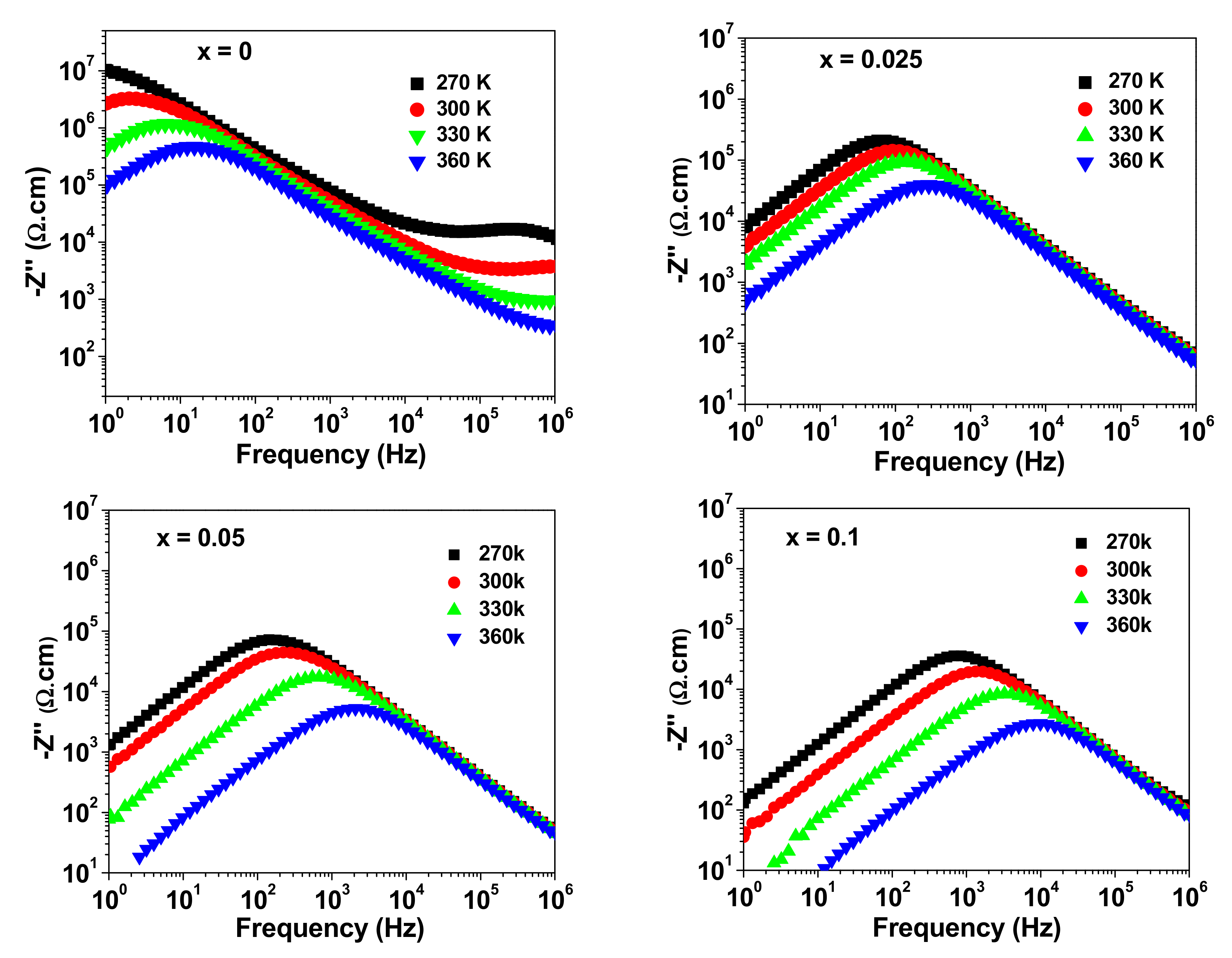
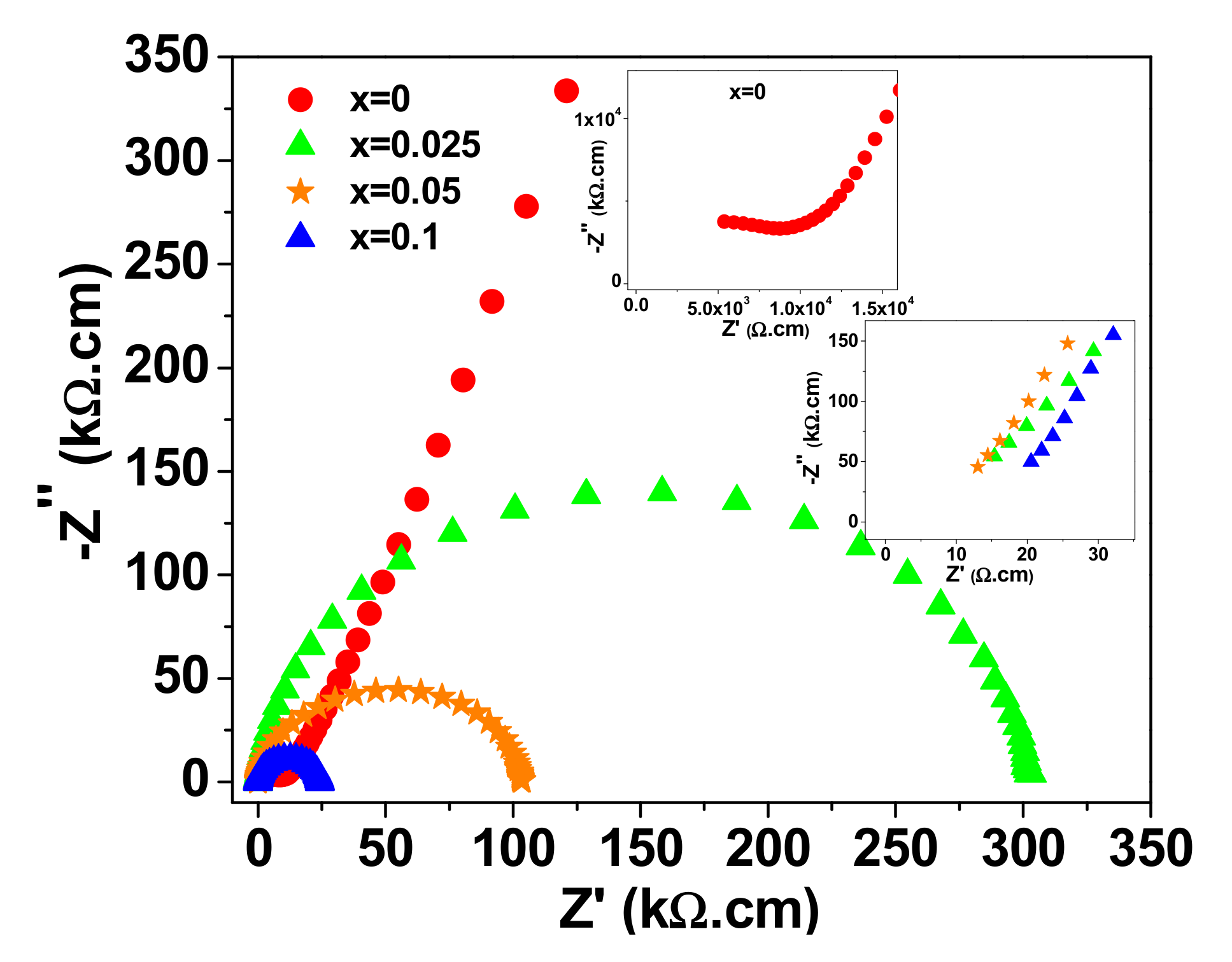
| Rg (Ω.cm) | Rgb (Ω.cm) | ε′ | tanδ | (tanδ)min | |
|---|---|---|---|---|---|
| at 1.1 kHz | |||||
| x = 0 | 1.2 × 10⁴ | 9.0 × 10⁶ | 1.1 × 10³ | 0.65 | 0.34 (at 58 Hz) |
| x = 0.025 | 15.3 | 3.0 × 10⁵ | 5.5 × 10⁴ | 0.18 | 0.11 (at 10 KHz) |
| x = 0.05 | 9.7 | 1.0 × 10⁵ | 6.0 × 10⁴ | 0.40 | 0.11 (at 24 KHz) |
| x = 0.1 | 35.9 | 4.3 × 10⁴ | 5.3 × 10⁴ | 1.37 | 0.13 (at 47 KHz) |
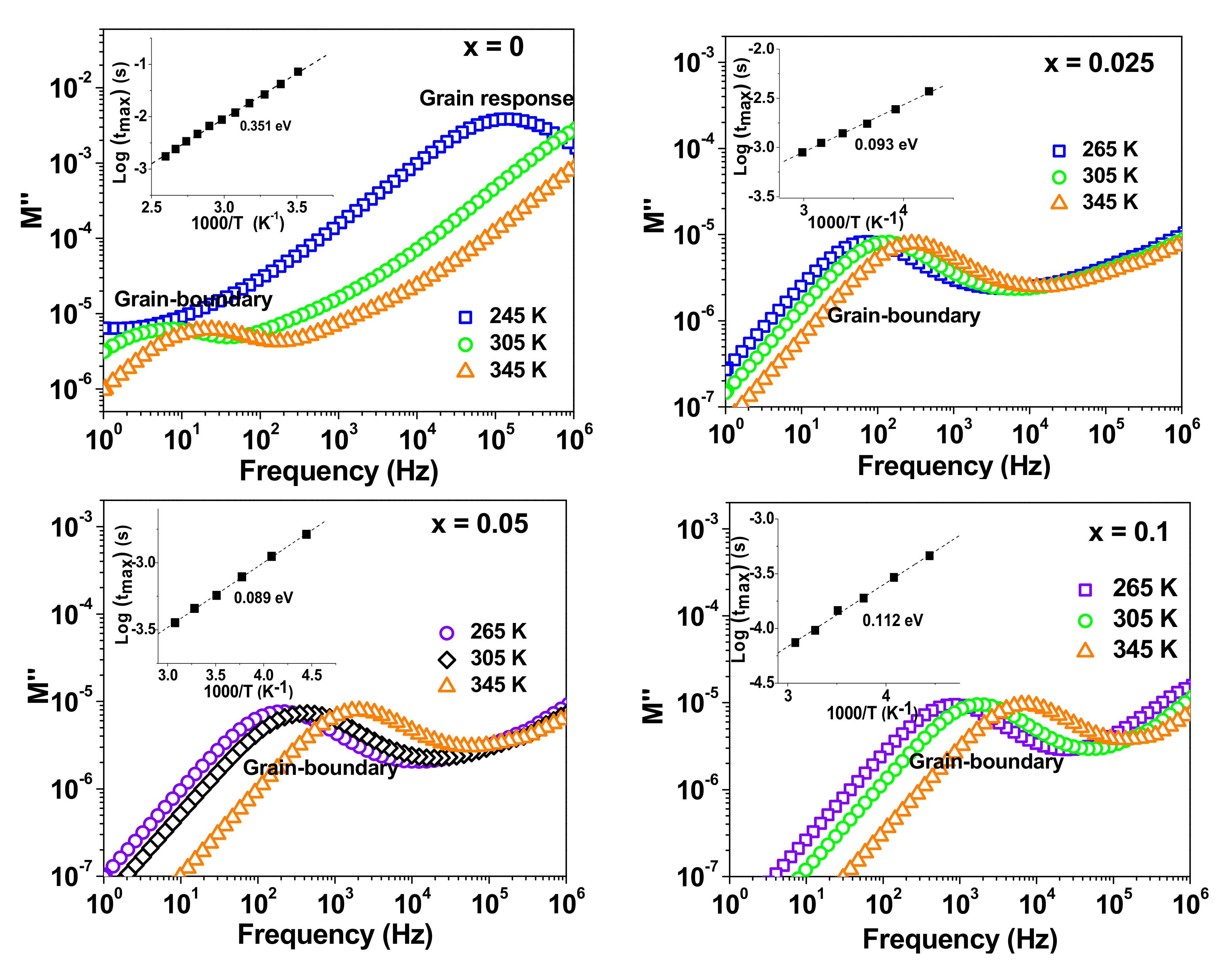
| E (eV) | U (eV) | |
|---|---|---|
| x = 0 | 0.338 | 0.341 |
| x = 0.025 | 0.089 | 0.095 |
| x = 0.05 | 0.087 | 0.078 |
| x = 0.1 | 0.101 | 0.099 |
Publisher’s Note: MDPI stays neutral with regard to jurisdictional claims in published maps and institutional affiliations. |
© 2022 by the authors. Licensee MDPI, Basel, Switzerland. This article is an open access article distributed under the terms and conditions of the Creative Commons Attribution (CC BY) license (https://creativecommons.org/licenses/by/4.0/).
Share and Cite
Kotb, H.M.; Alshoaibi, A.; Mazher, J.; Shaalan, N.M.; Ahmad, M.M. Colossal Permittivity Characteristics of (Nb, Si) Co-Doped TiO2 Ceramics. Materials 2022, 15, 4701. https://doi.org/10.3390/ma15134701
Kotb HM, Alshoaibi A, Mazher J, Shaalan NM, Ahmad MM. Colossal Permittivity Characteristics of (Nb, Si) Co-Doped TiO2 Ceramics. Materials. 2022; 15(13):4701. https://doi.org/10.3390/ma15134701
Chicago/Turabian StyleKotb, Hicham Mahfoz, Adil Alshoaibi, Javed Mazher, Nagih M. Shaalan, and Mohamad M. Ahmad. 2022. "Colossal Permittivity Characteristics of (Nb, Si) Co-Doped TiO2 Ceramics" Materials 15, no. 13: 4701. https://doi.org/10.3390/ma15134701
APA StyleKotb, H. M., Alshoaibi, A., Mazher, J., Shaalan, N. M., & Ahmad, M. M. (2022). Colossal Permittivity Characteristics of (Nb, Si) Co-Doped TiO2 Ceramics. Materials, 15(13), 4701. https://doi.org/10.3390/ma15134701